Table of Contents
Advertisement
Quick Links
Advertisement
Table of Contents

Related Manuals for Clevo P177SM-A


Summary of Contents for Clevo P177SM-A
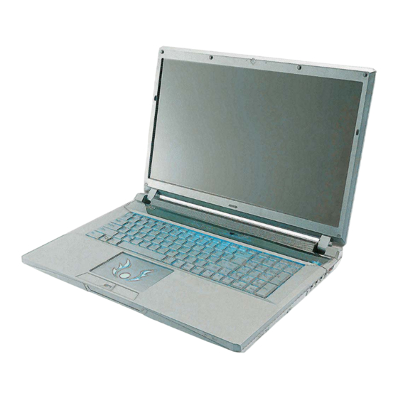
- Page 1 P177SM-A...
- Page 3 Preface Notebook Computer P177SM-A Service Manual...
- Page 4 Preface Notice The company reserves the right to revise this publication or to change its contents without notice. Information contained herein is for reference only and does not constitute a commitment on the part of the manufacturer or any subsequent ven- dor.
- Page 5 This manual is intended for service personnel who have completed sufficient training to undertake the maintenance and inspection of personal computers. It is organized to allow you to look up basic information for servicing and/or upgrading components of the P177SM-A series notebook PC.
- Page 6 Preface IMPORTANT SAFETY INSTRUCTIONS Follow basic safety precautions, including those listed below, to reduce the risk of fire, electric shock and injury to per- sons when using any electrical equipment: 1. Do not use this product near water, for example near a bath tub, wash bowl, kitchen sink or laundry tub, in a wet basement or near a swimming pool.
- Page 7 Preface Instructions for Care and Operation The notebook computer is quite rugged, but it can be damaged. To prevent this, follow these suggestions: Don’t drop it, or expose it to shock. If the computer falls, the case and the components could be damaged. Do not expose the computer Do not place it on an unstable Do not place anything heavy...
- Page 8 Preface Avoid interference. Keep the computer away from high capacity transformers, electric motors, and other strong mag- netic fields. These can hinder proper performance and damage your data. Take care when using peripheral devices. Removal Warning Use only approved brands of Unplug the power cord before When removing any peripherals.
- Page 9 Preface Battery Precautions • Only use batteries designed for this computer. The wrong battery type may explode, leak or damage the computer. • Do not continue to use a battery that has been dropped, or that appears damaged (e.g. bent or twisted) in any way. Even if the computer continues to work with a damaged battery in place, it may cause circuit damage, which may possibly result in fire.
- Page 10 Preface Related Documents You may also need to consult the following manual for additional information: User’s Manual on Disc This describes the notebook PC’s features and the procedures for operating the computer and its ROM-based setup pro- gram. It also describes the installation and operation of the utility programs provided with the notebook PC. System Startup 1.
-
Page 11: Table Of Contents
Preface Contents Introduction ..........1-1 Removing the Top Cover .............. 2-28 Part Lists ..........A-1 Overview ..................1-1 External Locator - Top View with LCD Panel Open ......1-4 Part List Illustration Location ............A-2 External Locator - Front & Right side Views .........1-5 Top with Fingerprint .............. - Page 12 Preface Lynix Point 1/9 ................B-20 Function LED Board ..............B-52 Lynix Point 2/9 ................B-21 Indicatory LED Board ..............B-53 Lynix Point3/9 ................B-22 P170 2nd HDD Board ..............B-54 Lynix Point 4/9 ................B-23 Power & LED Board ..............B-55 Lynix Point 5/9 ................B-24 P170 Click Board ................B-56 Lynix Point 6/9 ................
-
Page 13: Introduction
Chapter 1: Introduction Overview This manual covers the information you need to service or upgrade the P177SM-A series notebook computer. Informa- tion about operating the computer (e.g. getting started, and the Setup utility) is in the User’s Manual. Information about drivers (e.g. - Page 14 Introduction Specifications Storage Processor Options (Factory Option) One 12.7mm(h) Optical Device Type Intel® Core™ i7 Processor Drive (Super Multi Drive/Blu-Ray Combo Drive/Blu-Ray i7-4930MX (3.00GHz) Writer Drive) 8MB L3 Cache, 22nm, DDR3L-1600MHz, TDP 57W Two Changeable 2.5" (h) SATA (Serial) Hard Disk Drives Intel®...
-
Page 15: Overview
Introduction Audio Communication High Definition Audio Compliant Interface Built-In Gigabit Ethernet LAN S/PDIF Digital Output 2,0M FHD PC Camera Module Two Speakers WLAN/ Bluetooth Half Mini-Card Modules: One Sub Woofer (Factory Option) Intel® Centrino® Ultimate-N 6300 Wire- Built-In Microphone less LAN (802.11a/g/n) Sound Blaster Audio (Factory Option) Intel®... -
Page 16: External Locator - Top View With Lcd Panel Open
Introduction External Locator - Top View with LCD Panel Open Figure 1 Top View 1. Built-In PC Camera 2. PC Camera LED 3. Built-In Microphone 4. LCD 5. Speakers Note that Illuminated Touchpad has a defined valid 6. LED Indicators operational area of sensitivity 7. -
Page 17: External Locator - Front & Right Side Views
Introduction External Locator - Front & Right side Views Figure 2 Front Views 1. LED Power Indicators Figure 3 Right Side Views 1. Optical Device Drive Bay 2. Emergency Eject Hole 3. Headphone Jack 4. Microphone Jack 5. S/PDIF-Out Jack 6. -
Page 18: External Locator - Left Side & Rear View
Introduction External Locator - Left Side & Rear View Figure 4 Left Side View 1. Mini-IEEE 1394a Port 2. RJ-45 LAN Jack 3. USB 3.0 Port / USB Charge 4. USB 3.0 Port 5. Combined eSATA/ Powered USB 3.0 Port 6. -
Page 19: External Locator - Bottom View
Introduction External Locator - Bottom View Figure 6 Bottom View 1. Sub Woofer 2. Fan Outlet/Intake 3. Component Bay Cover 4. Primary HDD Bay 5. Secondary HDD 6. Battery Overheating To prevent your com- puter from overheating make sure nothing blocks the vent/fan in- takes while the com-... -
Page 20: Mainboard Overview - Top (Key Parts)
Introduction Mainboard Overview - Top (Key Parts) Figure 7 Mainboard Top Key Parts 1. Platform Controller Hub 2. Audio Codec 3. KBC ITE IT8587 1 - 8 Mainboard Overview - Top (Key Parts) -
Page 21: Mainboard Overview - Bottom (Key Parts)
Introduction Mainboard Overview - Bottom (Key Parts) Figure 8 Mainboard Bottom Key Parts 1. VGA-Card Connector 2. CPU Socket (no CPU installed) 3. Memory Slots DDR3L SO-DIMM (Primary) 4. Hard Disk Connector 5. MSATA Connector Mainboard Overview - Bottom (Key Parts) 1 - 9... -
Page 22: Mainboard Overview - Top (Connectors)
Introduction Mainboard Overview - Top (Connectors) Figure 9 Mainboard Top Connectors 1. USB 3.0 Port / e-SATA 2. Multi-in-1 Card Reader 3. KB LED Connector 4. TP LED Cable Connector 5. LED 4 Cable Connector 6. TouchPad Cable Connector 7. MSATA Cable Connector 8. -
Page 23: Mainboard Overview - Bottom (Connectors)
Introduction Mainboard Overview - Bottom (Connectors) Figure 10 Mainboard Bottom Connectors 1. DC-In Jack 2. Mini Display Port 3. HDMI-Out Port 4. Display Port 5. VGA Fan Cable Connector 6. Sub Woofer Cable Connector 7. CPU Fan Cable Connector 8. USB 3.0 Ports 9. - Page 24 Introduction 1 - 12...
-
Page 25: Disassembly
Chapter 2: Disassembly Overview This chapter provides step-by-step instructions for disassembling the P177SM-A series notebook’s parts and subsystems. When it comes to reassembly, reverse the procedures (unless otherwise indicated). We suggest you completely review any procedure before you take the computer apart. -
Page 26: Maintenance Tools
Disassembly NOTE: All disassembly procedures assume that the system is turned OFF, and disconnected from any power supply (the battery is removed too). Maintenance Tools The following tools are recommended when working on the notebook PC: • M3 Philips-head screwdriver •... -
Page 27: Maintenance Precautions
Disassembly Maintenance Precautions The following precautions are a reminder. To avoid personal injury or damage to the computer while performing a re- moval and/or replacement job, take the following precautions: Power Safety Warning 1. Don't drop it. Perform your repairs and/or upgrades on a stable surface. If the computer falls, the case and other Before you undertake components could be damaged. -
Page 28: Disassembly Steps
Disassembly Disassembly Steps The following table lists the disassembly steps, and on which page to find the related information. PLEASE PERFORM THE DISASSEMBLY STEPS IN THE ORDER INDICATED. To remove the Battery: To remove the Secondary System Memory: 1. Remove the battery page 2 - 5 1. -
Page 29: Removing The Battery
Disassembly Removing the Battery 1. Turn the computer off, and turn it over. 2. Slide the latch in the direction of the arrow (Figure 1a Figure 1 3. Slide the latch in the direction of the arrow, and hold it in place (Figure 1a Battery Removal 4. -
Page 30: Removing The Hard Disk Drive
Disassembly Removing the Hard Disk Drive Figure 2 HDD Assembly The hard disk drive can be taken out to accommodate other 2.5" serial (SATA) hard disk drives with a height of 9.5mm Removal (h). Follow your operating system’s installation instructions, and install all necessary drivers and utilities (as outlined in Chapter 4 of the User’s Manual) when setting up a new hard disk. - Page 31 Disassembly 4. Slide the HDD assembly in the direction of the arrow (Figure 3c Figure 3 5. Remove the hard disk assembly (Figure 3d HDD Assembly 6. Remove screws & and the insulation plate (Figure 3e Removal (cont’d.) 7. Reverse the process to install a new hard disk (do not forget to replace all the screws and covers). c.
- Page 32 Disassembly Hard Disk Size Note (Foam Rubber Insert) Note that the hard disks pictured on the following pages are all 9.5mm(H) hard disk drives. In some cases 7mm(H) hard disk drives will be installed. Figure 4 Foam Rubber Insert for 7mm(H) HDDs •...
-
Page 33: Removing The Ssd
Disassembly Removing the SSD Figure 5 SSD Removal 1. Turn off the computer, and remove the battery (page 2 - 5) and hard disk (page 2 - 2. Remove the screws from the shielding plate (Figure 5a a. Remove the screws. 3. -
Page 34: Removing The Optical (Cd/Dvd) Device
Disassembly Removing the Optical (CD/DVD) Device Figure 6 Optical Device 1. Turn off the computer, and remove the battery (page 2 - Removal 2. Locate the secondary hard disk bay cover and remove screws & (Figure 6a 3. Remove the hard disk bay cover and screw at point (Figure 6b a. - Page 35 Disassembly 6. Carefully pry the bezel off the optical device at point (Figure 7d Figure 7 7. Separate the bezel and the optical device. Optical Device 8. Reverse the process to attach the front bezel with the new optical device at point (Figure 7f).
-
Page 36: Removing The Hard Disk From The Secondary Hdd Bay
Disassembly Removing the Hard Disk from the Secondary HDD Bay Figure 8 Note that the secondary hard disk (if installed) is located under the optical device bay (CD/DVD). Secondary HDD Assembly Removal 1. Turn off the computer, and turn it over, remove the battery (page 2 - 5) and optical device (page 2 -... - Page 37 Disassembly 5. Remove screws and the insulation plate from the hard disk (Figure 9d). Figure 9 Secondary HDD Assembly Removal d. Remove the screws and the insulation plate. 6. Reverse the process to install a new disk (make sure you install the insulation plate). 7.
-
Page 38: Removing The Primary System Memory (Ram)
Disassembly Removing the Primary System Memory (RAM) Figure 10 RAM Module The computer has four memory sockets for 204 pin Small Outline Dual In-line (SO-DIMM) DDR 3L type memory modules Removal (see “Memory” on page 1 - 2 ). The total memory size is automatically detected by the POST routine once you turn on your a. - Page 39 Disassembly 5. Lift the component bay cover off the computer case. The modules will be visible at point (Figure 11d Figure 11 6. Gently pull the two release latches ( ) on the sides of the memory socket(s) in the direction indicated below &...
-
Page 40: Removing The Secondary System Memory (Ram)
Disassembly Removing the Secondary System Memory (RAM) Figure 12 RAM Module Memory Upgrade Process Removal 1. Turn off the computer, and turn it over, remove the battery (page 2 - 5), and component bay cover (page 2 - 14). a. Remove 2. - Page 41 Disassembly 5. Disconnect the keyboard ribbon cable and LED ribbon cable from the locking collar socket & by using Figure 13 a small flat-head screwdriver to pry the locking collar pins away from the base. (Figure 13e). RAM Module 6. Remove the keyboard and the memory sockets &...
-
Page 42: Removing The Wireless Lan Module
Disassembly Removing the Wireless LAN Module Figure 14 Wireless LAN 1. Turn off the computer, remove the battery (page 2 - 5) and the keyboard (page 2 - Module Removal 2. The Wireless LAN module will be visible at point under the keyboard (Figure 14a). -
Page 43: Wireless Lan, Combo, 3G & Lte Module Cables
Disassembly Wireless LAN, Combo, 3G & LTE Module Cables Note that the cables for connecting to the antennae on WLAN, WLAN & Bluetooth Combo, 3G and LTE modules are not labelled. The cables/covers (each cable will have either a black or transparent cable cover) are color coded for iden- tification as outlined in the table below. -
Page 44: Removing The Msata Module
Disassembly Removing the MSATA Module Figure 15 MSATA Module 1. Turn off the computer, remove the battery (page 2 - 5), and component bay cover (page 2 - 14). Removal 2. Locate the module, it is visible at point Figure 15a 3. -
Page 45: Removing And Installing The Processor
Disassembly Removing and Installing the Processor Figure 16 Processor Processor Removal Procedure Removal 1. Turn off the computer, remove the battery (page 2 - 5), and component bay cover (page 2 - 14). Procedure 2. Remove screws from the heat sink unit in the order indicated on the label (i.e screw 4 first through to screw 1 last Figure 16a) - Page 46 Disassembly 4. Turn the release latch towards the unlock symbol , to release the CPU (Figure 17c). Figure 17 5. Carefully (it may be hot) lift the CPU up out of the socket (Figure 17d). Processor Removal 6. See page 2 - 23 for information on inserting a new CPU.
- Page 47 Disassembly Processor Installation Procedure Figure 18 Processor 1. Insert the CPU , pay careful attention to the pin alignment (Figure 18a), it will fit only one way (DO NOT Installation FORCE IT!), and turn the release latch towards the lock symbol (Figure 18b).
-
Page 48: Removing And Installing The Video Card
Disassembly Removing and Installing the Video Card Figure 19 Video Card Video Card Removal Procedure Removal Procedure Turn off the computer, turn it over and remove the battery (page 2 - 5) and component cover (page 2 - Remove screws from the heat sink unit in the order indicated on the label (i.e screw 7 first through to screw a. - Page 49 Disassembly For video card (N15E-GX) additional removal procedure Figure 20 Remove screws from the video card assembly (Figure 20e) Video Card Separate the shielding plate from the video card (Figure 19d) Removal Procedure (cont’d.) e. Remove the screws. f. Separate shielding plate and video card.
- Page 50 Disassembly Installing a New Video Card Figure 21 Installing a New Prepare to fit the video card into the slot by holding it at about a 30° angle (Figure 21e). Video Card The card needs to be fully into the slot, and the video card and socket have a guide-key and pin which align to allow the card to fit securely (Figure 21f)
-
Page 51: Removing The Ccd
Disassembly Removing the CCD Figure 22 CCD Module 1. Turn off the computer, remove the battery (page 2 - Removal Remove the rubbers and screws (Figure 22a) 3. Run your fingers around the inner frame of the LCD panel at the points indicated by the arrows (Figure a. -
Page 52: Removing The Top Cover
Disassembly Removing the Top Cover Figure 23 Top Cover Removal 1. Turn off the computer, remove the battery (page 2 - 5), component bay cover (page 2 - 14), and keyboard (page 2 16). a. Disconnect cable Disconnect the cable connectors and c arefully lift the corresponding wires at the point from the holder as... - Page 53 Disassembly 5. Remove screws (Figure 24d). Figure 24 6. Lift the top cover at point (Figure 24e). Top Cover Removal 7. Carefully separate the top cover from the bottom case in the direction of the arrow at point . The hinge (cont’d) cover will automatically be released from its holder...
- Page 54 Disassembly 2 - 30...
-
Page 55: Part Lists
Part Lists Appendix A: Part Lists This appendix breaks down the P177SM-A series notebook’s construction into a series of illustrations. The component part numbers are indicated in the tables opposite the drawings. Note: This section indicates the manufacturer’s part numbers. Your organization may use a different system, so be sure to cross-check any relevant documentation. -
Page 56: Part List Illustration Location
Part Lists Part List Illustration Location The following table indicates where to find the appropriate part list illustration. Table A- 1 Part List Illustration Location Parts Top with Fingerprint page A - 3 Top without Fingerprint page A - 4 Bottom (N15E-GX) page A - 5 Bottom (N15P-GX) -
Page 57: Top With Fingerprint
Part Lists Top with Fingerprint Figure A - 1 Top with FOR 發光 Fingerprint FOR 無發光 ONLY FOR 發光 FOR 發光 FOR 無發光 Top with Fingerprint A - 3... -
Page 58: Top Without Fingerprint
Part Lists Top without Fingerprint FOR 發光 Figure A - 2 FOR 無發光 Top without Fingerprint ONLY FOR 發光 FOR 發光 FOR 無發光 A - 4 Top without Fingerprint... -
Page 59: Bottom (N15E-Gx
Part Lists Bottom (N15E-GX) Figure A - 3 Bottom (N15E-GX) Bottom (N15E-GX) A - 5... -
Page 60: Bottom (N15P-Gx
Part Lists Bottom (N15P-GX) Figure A - 4 Bottom (N15P-GX) A - 6 Bottom (N15P-GX) -
Page 61: Lcd
Part Lists Figure A - 5 LCD A - 7... -
Page 62: Combo
Part Lists COMBO Figure A - 6 COMBO A - 8 COMBO... -
Page 63: Dvd-Dual Drive
Part Lists DVD-Dual Drive Figure A - 7 DVD-Dual Drive DVD-Dual Drive A - 9... - Page 64 Part Lists A - 10...
-
Page 65: Schematic Diagrams
Schematic Diagrams Appendix B: Schematic Diagrams This appendix has circuit diagrams of the P177SM-A notebook’s PCB’s. The following table indicates where to find the appropriate schematic diagram. Diagram - Page Diagram - Page Diagram - Page Diagram - Page Table B - 1... -
Page 66: Block Diagram
Schematic Diagrams Block Diagram Sheet 1 of 66 Block Diagram B - 2 Block Diagram... -
Page 67: Processor 1/7
Schematic Diagrams Processor 1/7 Sheet 2 of 66 Processor 1/7 Processor 1/7 B - 3... - Page 68 Schematic Diagrams Processor 2/7 Sheet 3 of 66 Processor 2/7 B - 4 Processor 2/7...
-
Page 69: Processor 3/7
Schematic Diagrams Processor 3/7 Sheet 4 of 66 Processor 3/7 Processor 3/7 B - 5... - Page 70 Schematic Diagrams Processor 4/7 Sheet 5 of 66 Processor 4/7 B - 6 Processor 4/7...
-
Page 71: Processor 5/7
Schematic Diagrams Processor 5/7 Sheet 6 of 66 Processor 5/7 Processor 5/7 B - 7... - Page 72 Schematic Diagrams Processor 6/7 Sheet 7 of 66 Processor 6/7 B - 8 Processor 6/7...
-
Page 73: Processor 7/7
Schematic Diagrams Processor 7/7 Sheet 8 of 66 Processor 7/7 Processor 7/7 B - 9... -
Page 74: Ddr3 Cha So-Dimm_0
Schematic Diagrams DDR3 CHA SO-DIMM_0 Sheet 9 of 66 DDR3 CHA SO- DIMM _0 B - 10 DDR3 CHA SO-DIMM_0... -
Page 75: Ddr3 Cha So-Dimm_1
Schematic Diagrams DDR3 CHA SO-DIMM_1 Sheet 10 of 66 DDR3 CHA SO- DIMM _1 DDR3 CHA SO-DIMM_1 B - 11... -
Page 76: B - 12 Ddr3 Chb So-Dimm_1
Schematic Diagrams DDR3 CHB SO-DIMM_1 Sheet 11 of 66 DDR3 CHB SO- DIMM _1 B - 12 DDR3 CHB SO-DIMM_1... -
Page 77: Ddriii Chb So-Dimm_0
Schematic Diagrams DDRIII CHB SO-DIMM_0 Sheet 12 of 66 DDRIII CHB SO- DIMM _0 DDRIII CHB SO-DIMM_0 B - 13... -
Page 78: Mxm Pci-E
Schematic Diagrams MXM PCI-E Sheet 13 of 66 MXM PCI-E B - 14 MXM PCI-E... -
Page 79: Panel, Inverter, Crt
Schematic Diagrams Panel, Inverter, CRT Sheet 14 of 66 Panel, Inverter, Panel, Inverter, CRT B - 15... -
Page 80: Ps8625
Schematic Diagrams PS8625 Sheet 15 of 66 PS8625 B - 16 PS8625... -
Page 81: 1394A_Xio2221
Schematic Diagrams 1394a_XIO2221 Sheet 16 of 66 1394a_XIO2221 1394a_XIO2221 B - 17... -
Page 82: Display Port
Schematic Diagrams Display Port Sheet 17 of 66 Display Port B - 18 Display Port... -
Page 83: Hdmi
Schematic Diagrams HDMI Sheet 18 of 66 HDMI HDMI B - 19... - Page 84 Schematic Diagrams Lynix Point 1/9 Sheet 19 of 66 Lynix Point 1/9 B - 20 Lynix Point 1/9...
- Page 85 Schematic Diagrams Lynix Point 2/9 Sheet 20 of 66 Lynix Point 2/9 Lynix Point 2/9 B - 21...
-
Page 86: Lynix Point 1/9
Schematic Diagrams Lynix Point3/9 Sheet 21 of 66 Lynix Point 3/9 B - 22 Lynix Point3/9... -
Page 87: Lynix Point 4/9
Schematic Diagrams Lynix Point 4/9 Sheet 22 of 66 Lynix Point 4/9 Lynix Point 4/9 B - 23... -
Page 88: Lynix Point 5/9
Schematic Diagrams Lynix Point 5/9 Sheet 23 of 66 Lynix Point 5/9 B - 24 Lynix Point 5/9... -
Page 89: Lynix Point 8/9
Schematic Diagrams Lynix Point 6/9 Sheet 24 of 66 Lynix Point 6/9 Lynix Point 6/9 B - 25... - Page 90 Schematic Diagrams Lynix Point 7/9 Sheet 25 of 66 Lynix Point 7/9 B - 26 Lynix Point 7/9...
- Page 91 Schematic Diagrams Lynix Point 8/9 Sheet 26 of 66 Lynix Point 8/9 Lynix Point 8/9 B - 27...
- Page 92 Schematic Diagrams Lynix Point 9/9 Sheet 27 of 66 Lynix Point 9/9 B - 28 Lynix Point 9/9...
-
Page 93: Usb+Esata, Usb Charging
Schematic Diagrams USB+eSATA, USB Charging Sheet 28 of 66 USB+eSATA, USB Charging USB+eSATA, USB Charging B - 29... -
Page 94: Usb 2.0, Ccd, Mini Pcie, Lid
Schematic Diagrams USB 2.0, CCD, Mini PCIE, LID Sheet 29 of 66 USB 2.0, CCD, Mini PCIE, LED B - 30 USB 2.0, CCD, Mini PCIE, LID... -
Page 95: Led, Hotkey, Lid Sw, Fan
Schematic Diagrams LED, Hotkey, LID SW, Fan Sheet 30 of 66 LED, Hotkey, LID SW, Fan LED, Hotkey, LID SW, Fan B - 31... - Page 96 Schematic Diagrams RJ 45 Sheet 31 of 66 RJ 45 B - 32 RJ 45...
-
Page 97: Codec Realtek Alc892
Schematic Diagrams Codec Realtek ALC892 Sheet 32 of 66 Codec Realtek ALC892 Codec Realtek ALC892 B - 33... -
Page 98: Apa2607-Tpa2008D2
Schematic Diagrams APA2607-TPA2008D2 Sheet 33 of 66 APA2607- TPA2008D2 B - 34 APA2607-TPA2008D2... -
Page 99: Kbc-Ite It8587A
Schematic Diagrams KBC-ITE IT8587A Sheet 34 of 66 KBC-ITE IT8587A KBC-ITE IT8587A B - 35... -
Page 100: Backlight Keyboard
Schematic Diagrams Backlight Keyboard Sheet 35 of 66 Backlight Keyboard B - 36 Backlight Keyboard... -
Page 101: Msata, Fan, Tp, Fp, Multi-Con
Schematic Diagrams mSATA, FAN, TP, FP, MULTI-CON Sheet 36 of 66 mSATA, FAN, TP, FP, MULTI-CON mSATA, FAN, TP, FP, MULTI-CON B - 37... -
Page 102: Card Reader Rtl8411
Schematic Diagrams Card Reader RTL8411 Sheet 37 of 66 Card Reader RTL8411 B - 38 Card Reader RTL8411... -
Page 103: Usb 3.0
Schematic Diagrams USB 3.0 Sheet 38 of 66 USB 3.0 USB 3.0 B - 39... -
Page 104: Ddr 1.35V/0.75Vs Pch 1.5V
Schematic Diagrams DDR 1.35V/0.75VS PCH 1.5V Sheet 39 of 66 DDR 1.35V/0.75VS PCH 1.5V B - 40 DDR 1.35V/0.75VS PCH 1.5V... -
Page 105: Vdd3, Vdd5
Schematic Diagrams VDD3, VDD5 Sheet 40 of 66 VDD3, VDD5 VDD3, VDD5 B - 41... -
Page 106: 5Vs, 3.3V, 3.3Vs, 1.5Vs
Schematic Diagrams 5V, 5VS, 3.3V, 3.3VS, 1.5VS Sheet 41 of 66 5V, 5VS, 3.3V, 3.3VS, 1.5VS B - 42 5V, 5VS, 3.3V, 3.3VS, 1.5VS... -
Page 107: Power 1.05Vs
Schematic Diagrams Power 1.05VS Sheet 42 of 66 Power 1.05VS Power 1.05VS B - 43... -
Page 108: Led 5V
Schematic Diagrams LED 5V Sheet 43 of 66 LED 5V B - 44 LED 5V... -
Page 109: Power V-Core 1
Schematic Diagrams Power V-Core 1 Sheet 44 of 66 Power V-Core 1 Power V-Core 1 B - 45... -
Page 110: Ac_In, Charger
Schematic Diagrams AC_In, Charger Sheet 45 of 66 AC_In, Charger B - 46 AC_In, Charger... -
Page 111: Tpm
Schematic Diagrams Sheet 46 of 66 TPM B - 47... -
Page 112: Audio Board
Schematic Diagrams Audio Board Sheet 47 of 66 Audio Board B - 48 Audio Board... -
Page 113: P150 Odd Board
Schematic Diagrams P150 ODD Board Sheet 48 of 66 P150 ODD Board P150 ODD Board B - 49... -
Page 114: P150 Click Board
Schematic Diagrams P150 Click Board Sheet 49 of 66 P150 Click Board B - 50 P150 Click Board... -
Page 115: Power Led Board
Schematic Diagrams Power LED Board Sheet 50 of 66 Power LED Board Power LED Board B - 51... -
Page 116: Function Led Board
Schematic Diagrams Function LED Board Sheet 51 of 66 Function LED Board B - 52 Function LED Board... -
Page 117: Indicatory Led Board
Schematic Diagrams Indicatory LED Board Sheet 52 of 66 Indicatory LED Board Indicatory LED Board B - 53... -
Page 118: P170 2Nd Hdd Board
Schematic Diagrams P170 2nd HDD Board Sheet 53 of 66 P170 2nd HDD Board B - 54 P170 2nd HDD Board... -
Page 119: Power & Led Board
Schematic Diagrams Power & LED Board Sheet 54 of 66 Power & LED Board Power & LED Board B - 55... -
Page 120: P170 Click Board
Schematic Diagrams P170 Click Board Sheet 55 of 66 P170 Click Board B - 56 P170 Click Board... -
Page 121: P150 Fingerprint Board
Schematic Diagrams P150 Fingerprint Board Sheet 56 of 66 P150 Fingerprint Board P150 Fingerprint Board B - 57... -
Page 122: P170 Fingerprint Board
Schematic Diagrams P170 Fingerprint Board Sheet 57 of 66 P170 Fingerprint Board B - 58 P170 Fingerprint Board... -
Page 123: P150 2Nd Hdd Board
Schematic Diagrams P150 2nd HDD Board Sheet 58 of 66 P150 2nd HDD Board P150 2nd HDD Board B - 59... -
Page 124: Indicatory Led Board
Schematic Diagrams Indicatory LED Board Sheet 59 of 66 Indicatory LED Board B - 60 Indicatory LED Board... -
Page 125: Function Led Board
Schematic Diagrams Function LED Board Sheet 60 of 66 Function LED Board Function LED Board B - 61... -
Page 126: Mini-Dp
Schematic Diagrams Mini-DP Sheet 61 of 66 MIni-DP B - 62... -
Page 127: 2Nd Msata Board
Schematic Diagrams 2nd mSATA Board Sheet 62 of 66 2nd mSATA Board 2nd mSATA Board B - 63... -
Page 128: Power On / S4 Resume Seq
Schematic Diagrams Power on / S4 Resume Seq. Sheet 63 of 66 Power on / S4 Resume Seq. B - 64 Power on / S4 Resume Seq. -
Page 129: S3 Resume Seq
Schematic Diagrams S3 Resume Seq. Sheet 64 of 66 S3 Resume Seq. S3 Resume Seq. B - 65... -
Page 130: Into S3 Sequence
Schematic Diagrams Into S3 Sequence Sheet 65 of 66 Into S3 Sequence B - 66 Into S3 Sequence... -
Page 131: Into S4 Sequence
Schematic Diagrams Into S4 Sequence Sheet 66 of 66 Into S4 Sequence Into S4 Sequence B - 67... - Page 132 Schematic Diagrams B - 68...
-
Page 133: Updating The Flash Rom Bios
Download the BIOS computer model. 1. Go to www.clevo.com.tw and point to E-Services and click E-Channel. Note that BIOS versions 2. Use your user ID and password to access the appropriate download area (BIOS), and download the latest BIOS files... - Page 134 BIOS Update Use the flash tools to update the BIOS 1. Make sure you are not loading any memory management programs such as HIMEM by holding the F8 key as you see the message “Starting MS-DOS”. You will then be prompted to give “Y” or “N” responses to the programs being loaded by DOS.
Need help?
Do you have a question about the P177SM-A and is the answer not in the manual?
Questions and answers