Table of Contents
Advertisement
Quick Links
Service
Manual
SECTION
1. TECHNICAL SPECIFICATIONS .................................................................................................... 1
2. SERVICE MODE ............................................................................................................................ 2
3. MAIN MICROPROCESSOR (Q120) UPDATE PROCEDURE ....................................................... 3
4. WIRING DIAGRAM ........................................................................................................................ 5
5. BLOCK DIAGRAM ......................................................................................................................... 6
6. SCHEMATIC DIAGRAM ................................................................................................................. 7
7. PARTS LOCATION ...................................................................................................................... 19
8. EXPLODED VIEW AND PARTS LIST ......................................................................................... 31
9. MICROPROCESSOR AND IC DATA ........................................................................................... 34
10. ELECTRICAL PARTS LIST .......................................................................................................... 53
Please use this service manual with referring to the user guide ( D.F.U. ) without fail.
All manuals and user guides at all-guides.com
TABLE OF CONTENTS
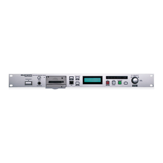
PMD560
PMD560 /
N1S/U1S
Solid State Recorder
PAGE
Part no. 90M39BS855010
F i r s t I s s u e 2 0 0 5 . 1 2
ecm
Advertisement
Table of Contents

Related Manuals for Marantz PMD560


Summary of Contents for Marantz PMD560
-
Page 1: Table Of Contents
All manuals and user guides at all-guides.com Service PMD560 / N1S/U1S Manual Solid State Recorder TABLE OF CONTENTS SECTION PAGE 1. TECHNICAL SPECIFICATIONS ....................1 2. SERVICE MODE ..........................2 3. MAIN MICROPROCESSOR (Q120) UPDATE PROCEDURE ............3 4. WIRING DIAGRAM ........................5 5. - Page 2 All manuals and user guides at all-guides.com SHOCK, FIRE HAZARD SERVICE TEST : CAUTION : After servicing this appliance and prior to returning to customer, measure the resistance between either primary AC cord connector pins ( with unit NOT connected to AC mains and its Power switch ON ), and the face or Front Panel of product and controls and chassis bottom.
-
Page 3: Technical Specifications
All manuals and user guides at all-guides.com 1. TECHNICAL SPECIFICATIONS Digital audio system Included accessories System..........Solid State Recorder Power cord Compatible media ........CF memory cards Americas model ............... 1 Microdrive Europe model ..............2 USB cable ................1 Recording and media methods Audio cable ................ -
Page 4: Service Mode
All manuals and user guides at all-guides.com 2. SERVICE MODE 2. SERVICE 1. Micro-Processor(Q120) VERSION 1. Micro-Processor(Q120) Version check 1) Press POWER switch on the unit. 1) POWER 2) MENU/STORE 2) Press MENU/STORE button. 3) Preset-1 is displayed on LCD. 3) DISPLAY Preset-1 MARK... -
Page 5: Main Microprocessor (Q120) Update Procedure
CompactFlash (with format) • CompactFlash Update Disc (90M-PMD560CDR) • (90M-PMD560CDR) • Connection 1. Connect Windows PC and PMD560 with USB cable 1. Windows PC PMD560 2. Insert the CompactFlash PMD560 Writing procedure When you have already written the update file in CompactFlash CompactFlash, please go to No9. - Page 6 PMD560 9. After "Update" is displayed for a second on the display 9. PMD560 Update of PMD560, the version number of the higher version is displayed, and the display "OK?" blinks at the same time. "OK?" MARK S.SKIP...
-
Page 7: Wiring Diagram
All manuals and user guides at all-guides.com 4. WIRING DIAGRAM... -
Page 8: Block Diagram
All manuals and user guides at all-guides.com 5. BLOCK DIAGRAM... -
Page 9: Schematic Diagram
All manuals and user guides at all-guides.com 6. SCHEMATIC DIAGRAM R566 R587 C553 OPEN C576 C536 100p Q512 J506 R542 4.7K Q508 NJM2068M C582 R595 B8B-PH-K-S NJM2068M 10u/16V TPF544 D500 C557 10u/16V LCH_IN DAN202K C549 C539 R552 10u/16V 0.1u OPEN GND_A C578 TPF545... - Page 10 All manuals and user guides at all-guides.com Q713 R769 NJM2387DL2 P203 00MWG39BS2030 1/10W VADJ 4 CNT 2 POWER UNIT R731 D_GND 1/10W Q706 L705 BD9778/HFP 100uH TPF706 R728 R732 J705 150k 1/10W C723 B6B-PH-K-S 4700p TPF707 D_GND D_GND D_GND R725 D_GND TPF708 R799...
- Page 11 All manuals and user guides at all-guides.com +3.3V R663 D652 SML-512UW (RD) L-OVER P204 00MWG39BS2040 TPF658 P202 00MWG39BS2020 R664 D653 SML-512DW HP JACK UNIT PANEL UNIT TPF659 R665 D654 SML-512DW (ORG) TPF660 R666 D655 SML-512DW C805 R810 TPF661 TPF800 OPEN (MUTE_ON) R667 D656...
- Page 12 Q125 TC74LCX14FT R198 0.1u AN11 ENCORDERA AN12 R861 AN13 *JOGSW AN14 ENCORDERB GND SDA Q125 (4/6) AN15 Q117 *DOOR AN16 LH28F800BJE(PMD560) Q119 R860 LCD_nRES AN17 Q116 CDCV304PW L128 LCD_RS AVRFEM UPD444012AGY R347 LCD_R/W AVSS CKIN R267 R348 LCD_E BYTE MODE1...
- Page 13 All manuals and user guides at all-guides.com MAIN UNIT(2/3) P101 00MWI39BS1010 J113 R385 TP266 R386 TP267 R387 TP268 +3.3V_DSY +3.3V_DCF TP269 D_GND D_GND +3.3V_DSY CPLD_nRES CF_CLK C270 J109 100u/10V SCFB3A0400 C271 TP203 0.01u C272 0.1u TP155 +3.3V_DSY C_D3 C_D3 R404 TP156 C_D4 D_GND...
- Page 14 All manuals and user guides at all-guides.com MAIN UNIT(3/3) 2125 P101 00MWI39BS1010 R497 +5V_DLC +5V_DLC J100 2125 2125 Q128 BLM11B601S R102 R135 53398-0371 OPEN L100 TP281 TP290 LEDA VADJ TP282 LEDK BLM11B601S L101 D_GND R150 OPEN +3.3V_DSY C129 2125 2125 10u/16V Q100 R480...
-
Page 15: Parts Location
All manuals and user guides at all-guides.com 7. PARTS LOCATION P101 A C100 F1 C239 B9 J112 E9 R144 E10 R280 E8 C101 F1 C240 B9 J113 A1 R145 E10 R281 E8 C102 F2 C241 B9 L102 D11 R146 E10 R282 F5 C103 F2 C242 B9... - Page 16 All manuals and user guides at all-guides.com P101 B C104 E1 C214 F5 L131 D7 R235 F5 R377 D4 C105 E1 C215 F6 L132 D7 R236 B5 R378 D4 C113 D4 C216 F5 L136 B5 R237 B5 R379 D4 C137 C4 C217 F5 L137 D8 R238 B5...
- Page 17 All manuals and user guides at all-guides.com P201 A C500 D10 C569 D7 Q510 B10 R563 B2 C501 D10 C570 D7 Q511 C7 R564 A2 C502 D9 C571 B6 Q512 B6 R566 B9 C503 D9 C572 C7 Q513 B7 R567 B10 C504 D4 C573 C7 Q516 C3...
- Page 18 All manuals and user guides at all-guides.com P202 A C650 B4 D657 B9 Q650 B5 R665 B10 R685 B8 C651 B4 D658 B9 Q651 B6 R666 B9 R686 B7 C652 B4 D659 B8 R647 B4 R667 B9 R687 A8 C653 B5 D660 B8 R648 B4 R668 B9...
- Page 19 All manuals and user guides at all-guides.com P203 A C701 B3 D713 H9 R717 F8 R777 H9 C702 E3 D714 D8 R718 G8 R778 H9 C703 E3 D715 D10 R719 F8 R779 H9 C704 E2 D716 E10 R720 F8 R780 G10 C705 G4 D717 G7 R721 E8...
- Page 20 All manuals and user guides at all-guides.com P203 B P207 A D970 A1 J970 A2 R970 A1 P207 B Sn-Ag-Cu Lead-free Solder When soldering, use the Lead-free Solder (Sn-Ag-Cu).
-
Page 21: Exploded View And Parts List
All manuals and user guides at all-guides.com 8. EXPLODED VIEW AND PARTS LIST 5128 ø3X8(U) 5110 ø3X6(A) P203 5110 ø3X6(A) 5128 ø4X8(U) 030G 028G 5110 ø3X6(A) 015Gx3 002D P101 040G P201 5128 ø3X8(U) 006D Z10Z 010G 5405 ø4(R) J701 008G P204 007G 026G... - Page 22 002S 00M39BS801010 PACKING CASE PACKING CASE PMD560 004S 00M39BS809010 CUSHION CUSHION L 005S 00M39BS809020 CUSHION CUSHION R 002D 00M14AS257030 TOP COVER 006D 00M49AS253010 HANDLE HANDLE NOTE : "nsp" PART IS LISTED FOR REFERENCE ONLY, MARANTZ WILL NOT SUPPLY THESE PARTS.
-
Page 23: Microprocessor And Ic Data
All manuals and user guides at all-guides.com 9. MICROPROCESSOR AND IC DATA Q120 : µPD703111AGM (MAIN uP) 1/3 PMD560 PORT Connection Function I/O DET Ext Ini Res JIT1 JIT1 – MODE SELECT for SSCG JIT0 JIT0 – MODE SELECT for SSCG... - Page 24 All manuals and user guides at all-guides.com Q120 : µPD703111AGM (MAIN uP) 2/3 63 A11 – – – – EXT. MEMORY ADDRESS BUS11 ROM/RAM 64 A10 – – – – EXT. MEMORY ADDRESS BUS10 ROM/RAM 65 A9 – – – –...
- Page 25 All manuals and user guides at all-guides.com Q120 : µPD703111AGM (MAIN uP) 3/3 PDH10/D26/_INTPD10/ PDH10 – – – – JOG B INTP110/TCUD11 PDH11/D27/_INTPD11/ PDH11 – – – – JOG PUSH INTP111/TCLD11 126 PDH12/D28/_INTPD12/TO11 – – – – USB IN CONNECTER PDH13/D29/_INTPD13/ PDH13 –...
- Page 26 All manuals and user guides at all-guides.com Q119 : CDCV304PW(140-MHz PCI-X CLOCK BUFFER) FUNCTION TABLE INPUTS OUTPUT CLKIN 1Y (0:3) functional block diagram Logic Control CLKIN Q121 : NJU6350B(REAL TIME CLOCK)
- Page 27 All manuals and user guides at all-guides.com Q123 : AK4537(CODEC)
- Page 28 All manuals and user guides at all-guides.com Q123 : AK4537(CODEC)
- Page 29 All manuals and user guides at all-guides.com Q124 : µPD77115 (DSP)
- Page 30 All manuals and user guides at all-guides.com Q108 : MN1382S-H Block Diagram Voltage Reference 1 Comparator – Level Converter Output Circuit Comparator Voltage – Reference 2 Note * 1 : Circuits vary slightly depending on the output type (CMOS output, N-channel open drain output, or inverted CMOS output) Pin Descriptions Pin No.
- Page 31 All manuals and user guides at all-guides.com Q110 : TC74LCX125FT Q121 : TC74LCX08FT Q125 : TC74LCX14FT Q130, 132 : TC74LCX00FT...
- Page 32 All manuals and user guides at all-guides.com Q507 : BU4052BCF Block diagram COMMON OUT / IN COMMON OUT / IN Logic circuit diagram Truth table ON SWITCH (16) INH (6) BINARY TO 1of 4 LEVEL A (10) CONVERTER DECODER WITH INH B (9) NONE X: Irrelevant...
- Page 33 All manuals and user guides at all-guides.com Q511 : TC9459BFG TC9459BFG L-OUT R-OUT L-IN R-IN L-ch R-ch L-LD1 R-LD1 L-LD2 R-LD2 L-A-GND R-A-GND DATA L-OUT 3 R-OUT NC 4 91STEP L-IN 5 R-IN Same as L-ch Circuit L-LD1 6 R-LD1 L-LD2 7 R-LD2 L-A-GND 8...
- Page 34 All manuals and user guides at all-guides.com Q511 : TC9459BFG...
- Page 35 All manuals and user guides at all-guides.com Q516 : µPD4721GS-GJG PD4721GS-GJG +10V +3.3V -10V STBY Note 4 300Ω INT1 OUT1 300Ω INT2 OUT2 OUT1 5.5kΩ OUT2 5.5kΩ Q708 : BA9741FS-E2...
- Page 36 All manuals and user guides at all-guides.com Q650, Q651 : NJU3716AM DATA DATA NJU3716AM Controller Circuit TERMINAL DESCRIPTION SYMBOL FUNCTION Parallel Conversion Data Output Terminals Parallel Conversion Data Output Terminals Serial Data Output Terminal DATA Serial Data Input Terminal Clock Signal Input Terminal Strobe Signal Input Terminal Clear Signal Input Terminal Parallel Conversion Data Output Terminal...
- Page 37 All manuals and user guides at all-guides.com Q701 : MIP3E50MY 1 : Control 2 : Control 3 : Drain TO-220-A1 Package At startup Startup constant current Drain Control 1 Light load detection Internal power supply For intermittent oscillation control Timer intermittent operation circuit Overheat Error amplifier...
- Page 38 All manuals and user guides at all-guides.com Q706 : BD9778HFP ON/OFF L : OFF H : ON Vref SOFT START ERROR AMP COMPARATR DRIVER LATCH RESET CURRENT LIMT Refer to the Technical Note about the details of the application. Pin No. Pin Name...
- Page 39 All manuals and user guides at all-guides.com Q711 : µPD78F9222 NOTE P20/ANI0 P121/X1 P21/ANI1 P122/X2 P123 P22/ANI2 P23/ANI3 P130 RESET/P34 P31/T1010/TO00/INTP2 P30/TI000/INTP3 P44/RxD6 P43/TxD6INTP1 P41/INTP3 P42/TOH1 ANI0 to ANI3: Analog input RESET: Reset Analog reference voltage RxD6: Receive data INTP0 to INTP3: External interrupt input TI000, TI010: Timer input...
- Page 40 All manuals and user guides at all-guides.com Q711 : µPD78F9222 (1) Port functions Pin Name Function After Reset Alternate- Function Pin P20 to P23 Port 2. Input ANI0 to ANI3 4-bit I/O port. Can be set to input or output mode in 1-bit units. An on-chip pull-up resistor can be connected by setting software.
- Page 41 All manuals and user guides at all-guides.com Q711 : µPD78F9222 (2) Non-port functions Pin Name Function After Reset Alternate- Function Pin INTP0 Input External interrupt input for which the valid edge (rising edge, Input P30/TI000 falling edge, or both rising and falling edges) can be specified INTP1 P43/TxD6 INTP2...
-
Page 42: Electrical Parts List
All manuals and user guides at all-guides.com 10. ELECTRICAL PARTS LIST NOTE ON SAFETY FOR FUSIBLE RESISTOR : PARTS INFORMATION RESISTORS The suppliers and their type numbers of fusible resistors 1) 00MGD05 × × × 140, Carbon film fixed resistor, ±5% 1/4W are as follows;... - Page 43 00MDD95150300 CER. CAP. 15 PF +- 5 % CG 50V GR39 P101 C161 00MDK96103300 CER. CAP. 0.01UF +-10% 50V C1608JB1H103K P101 C162 00MDK98104200 CER. CAP. GRM39F104Z16 0.1UF NOTE : "nsp" PART IS LISTED FOR REFERENCE ONLY, MARANTZ WILL NOT SUPPLY THESE PARTS.
- Page 44 00MDD95560300 CER. CAP. 56PF (GR39) P101 C236 00MDD95560300 CER. CAP. 56PF (GR39) P101 C237 00MDD95560300 CER. CAP. 56PF (GR39) P101 C238 00MDD95560300 CER. CAP. 56PF (GR39) NOTE : "nsp" PART IS LISTED FOR REFERENCE ONLY, MARANTZ WILL NOT SUPPLY THESE PARTS.
- Page 45 00MHZ30014060 00MHZ30014060 CHIP DIODE NNCD4.3C ESD NOISE CLIPPING DIODES P101 D117 00MHZ30012060 00MHZ30012060 CHIP DIODE NSAD500F SURGE ABSORBER P101 D118 00MHZ30012060 00MHZ30012060 CHIP DIODE NSAD500F SURGE ABSORBER NOTE : "nsp" PART IS LISTED FOR REFERENCE ONLY, MARANTZ WILL NOT SUPPLY THESE PARTS.
- Page 46 DTC114EU P101 Q116 00D2623469000 00D2623469000 IC UPD444012AGY-B55X P101 Q117 00MHC1005532F 00MHC1005532F U-PRO LH28F800BJE(PMD560) P101 Q118 00D2623114902 00D2623114902 IC S-24C01BFJ-TB P101 Q119 00MHC10144370 00MHC10144370 IC CDCV304PWR NOTE : "nsp" PART IS LISTED FOR REFERENCE ONLY, MARANTZ WILL NOT SUPPLY THESE PARTS.
- Page 47 10K OHM +- 5% 1/16W P101 R160 00MNN05102610 CHIP RES. 1K OHM +- 5% 1/16W P101 R161 00MNN05473610 CHIP RES. 47K OHM +- 5% 1/16W NOTE : "nsp" PART IS LISTED FOR REFERENCE ONLY, MARANTZ WILL NOT SUPPLY THESE PARTS.
- Page 48 0 OHM +- 5% 1/16W P101 R225 00MNN05220610 CHIP RES. 22 OHM +- 5% 1/16W P101 R226 00MNN05000610 CHIP RES. 0 OHM +- 5% 1/16W NOTE : "nsp" PART IS LISTED FOR REFERENCE ONLY, MARANTZ WILL NOT SUPPLY THESE PARTS.
- Page 49 330 OHM +- 5% 1/16W P101 R293 00MNN05331610 CHIP RES. 330 OHM +- 5% 1/16W P101 R294 00MNN05331610 CHIP RES. 330 OHM +- 5% 1/16W NOTE : "nsp" PART IS LISTED FOR REFERENCE ONLY, MARANTZ WILL NOT SUPPLY THESE PARTS.
- Page 50 330 OHM +- 5% 1/16W P101 R363 00MNN05331610 CHIP RES. 330 OHM +- 5% 1/16W P101 R364 00MNN05331610 CHIP RES. 330 OHM +- 5% 1/16W NOTE : "nsp" PART IS LISTED FOR REFERENCE ONLY, MARANTZ WILL NOT SUPPLY THESE PARTS.
- Page 51 330 OHM +- 5% 1/16W P101 R426 00MNN05331610 CHIP RES. 330 OHM +- 5% 1/16W P101 R427 00MNN05331610 CHIP RES. 330 OHM +- 5% 1/16W NOTE : "nsp" PART IS LISTED FOR REFERENCE ONLY, MARANTZ WILL NOT SUPPLY THESE PARTS.
- Page 52 47K OHM +- 5% 1/16W P101 R497 00MNI05000110 00MNI05000110 CHIP RES. 0 OHM +- 5% 1/10W P101 R498 00MNN05000610 CHIP RES. 0 OHM +- 5% 1/16W NOTE : "nsp" PART IS LISTED FOR REFERENCE ONLY, MARANTZ WILL NOT SUPPLY THESE PARTS.
- Page 53 00MDK98104200 CER. CAP. GRM39F104Z16 0.1UF P201 C523 00MDK98104200 CER. CAP. GRM39F104Z16 0.1UF P201 C524 00MDK98104200 CER. CAP. GRM39F104Z16 0.1UF P201 C525 00MDK98104200 CER. CAP. GRM39F104Z16 0.1UF NOTE : "nsp" PART IS LISTED FOR REFERENCE ONLY, MARANTZ WILL NOT SUPPLY THESE PARTS.
- Page 54 00MFC90020110 00MFC90020110 FERRITE CORE BLM11B601S CHIP FERRITE P201 L505 00MFC90020110 00MFC90020110 FERRITE CORE BLM11B601S CHIP FERRITE P201 L506 00MFC90020110 00MFC90020110 FERRITE CORE BLM11B601S CHIP FERRITE NOTE : "nsp" PART IS LISTED FOR REFERENCE ONLY, MARANTZ WILL NOT SUPPLY THESE PARTS.
- Page 55 10K OHM +- 5% 1/16W P201 R539 00MNN05103610 CHIP RES. 10K OHM +- 5% 1/16W P201 R540 00MNN05332610 CHIP RES. 3.3K OHM +- 5% 1/16W NOTE : "nsp" PART IS LISTED FOR REFERENCE ONLY, MARANTZ WILL NOT SUPPLY THESE PARTS.
- Page 56 22 OHM +- 5% 1/16W P201 R616 00MNN05220610 CHIP RES. 22 OHM +- 5% 1/16W P201 R617 00MNN05220610 CHIP RES. 22 OHM +- 5% 1/16W NOTE : "nsp" PART IS LISTED FOR REFERENCE ONLY, MARANTZ WILL NOT SUPPLY THESE PARTS.
- Page 57 22 OHM +- 5% 1/16W P202 R653 00MNN05220610 CHIP RES. 22 OHM +- 5% 1/16W P202 R654 00MNN05331610 CHIP RES. 330 OHM +- 5% 1/16W NOTE : "nsp" PART IS LISTED FOR REFERENCE ONLY, MARANTZ WILL NOT SUPPLY THESE PARTS.
- Page 58 47 UF M 25V RA-2 P203 ! C710 00MDK17471520 00MDK17471520 CER. CAP. ! DE0910 B 471K -KX 470PF 250V P203 C711 00MDK98104200 CER. CAP. GRM39F104Z16 0.1UF NOTE : "nsp" PART IS LISTED FOR REFERENCE ONLY, MARANTZ WILL NOT SUPPLY THESE PARTS.
- Page 59 ! MIP3E50MY ! Q702 P203 00MHC33036590 00MHC33036590 IC ! TL431CZ PROG.VOLTAGE REFERENCE P203 Q703 00MBA20035210 00MBA20035210 TRS. DTC114EU P203 Q704 00MHX300012B0 00MHX300012B0 CHIP TRS. 2SC4081(R.S) 2SC4116(GR.BL) NOTE : "nsp" PART IS LISTED FOR REFERENCE ONLY, MARANTZ WILL NOT SUPPLY THESE PARTS.
- Page 60 18K OHM +- 5% 1/16W P203 R752 00MNN05221610 CHIP RES. 220 OHM +- 5% 1/16W P203 R753 00MNN05221610 CHIP RES. 220 OHM +- 5% 1/16W NOTE : "nsp" PART IS LISTED FOR REFERENCE ONLY, MARANTZ WILL NOT SUPPLY THESE PARTS.
- Page 61 00MYJ01080220 00MYJ01080220 JACK YKB21-5265 6.3MM STEREO PHONE P204 L801 00MFC90020110 00MFC90020110 FERRITE CORE BLM11B601S CHIP FERRITE P204 L802 00MFC90020110 00MFC90020110 FERRITE CORE BLM11B601S CHIP FERRITE NOTE : "nsp" PART IS LISTED FOR REFERENCE ONLY, MARANTZ WILL NOT SUPPLY THESE PARTS.
- Page 62 EC11B20244 V L=15MM STB LED UNIT PWB P207 (00MWG39BS207-) P207 D970 00MHI10125210 00MHI10125210 L.E.D. SML-311BBT P207 R970 00MNN05181610 CHIP RES. 180 OHM +- 5% 1/16W NOTE : "nsp" PART IS LISTED FOR REFERENCE ONLY, MARANTZ WILL NOT SUPPLY THESE PARTS.
Need help?
Do you have a question about the PMD560 and is the answer not in the manual?
Questions and answers