Table of Contents
Advertisement
Quick Links
Download this manual
See also:
User Manual
Advertisement
Table of Contents

Related Manuals for Supero P8SGA

Summary of Contents for Supero P8SGA
- Page 1 UPER P8SGA USER’S MANUAL Revision 1.1a...
- Page 2 Please Note: For the most up-to-date version of this manual, please see our web site at www.supermicro.com. SUPER MICRO COMPUTER reserves the right to make changes to the product described in this manual at any time and without notice.
-
Page 3: About This Manual
Manual Organization Chapter 1 includes a checklist of what should be included in your mainboard box, describes the features, specifi cations and performance of the P8SGA mainboard and provides detailed information about the chipset. Chapter 2 begins with instructions on handling static-sensitive devices. Read this chapter when installing the processor and DDR memory modules and when mounting the mainboard in the chassis. -
Page 4: Table Of Contents
Chapter 1: Introduction Overview ... 1-1 Checklist ... 1-1 Contacting Supermicro ... 1-2 SUPER P8SGAImage ... 1-3 P8SGA Layout ... 1-4 P8SGAQuick Reference ... 1-5 E7205 Chipset: System Block Diagram ... 1-6 Motherboard Features ... 1-7 Chipset Overview ... 1-9 PC Health Monitoring ... - Page 5 Serial Ports ... 2-12 CD Header ... 2-12 Fan Headers ... 2-13 Chassis Intrusion ... 2-13 ATX PS/2 Keyboard/Mouse Ports ... 2-14 Universal Serial Bus (USB) ... 2-14 Wake-On-Ring ... 2-15 Wake-On-LAN ... 2-15 Ethernet Port ... 2-15 VGA Connector ... 2-16 SMB Header ...
- Page 6 P8SGA User’s Manual Chapter 4: BIOS Introduction ... 4-1 Running Setup ... 4-2 Main BIOS Setup ... 4-2 Main BIOS Setup Menu ... 4-3 Advanced BIOS Setup ... 4-5 4-4.1 Advanced BIOS Features ... 4-5 4-4.2 Advanced Chipset Control ... 4-7 4-4.3 I/O Device Confi...
-
Page 7: Chapter 1: Introduction
Checklist Congratulations on purchasing your computer motherboard from an acknowledged leader in the industry. Supermicro boards are designed with the utmost attention to detail to provide you with the highest standards in quality and performance. Please check that the following items have all been included with your motherboard. -
Page 8: Contacting Supermicro
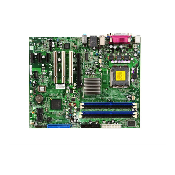
P8SGA User’s Manual Contacting Super Micro Headquarters Address: Super Micro Computer, Inc. 980 Rock Ave. San Jose, CA 95131 U.S.A. Tel: +1 (408) 503-8000 Fax: +1 (408) 503-8008 Email: marketing@supermicro.com (General Information) support@supermicro.com (Technical Support) Web Site: www.supermicro.com Europe Address: Super Micro Computer B.V. - Page 9 • All images, layouts and contents included in this manual were based upon the latest PCB revision available at the time of publishing of this manual. The moth- erboard you've received may or may not look exactly the same as the graphics shown in this manual. P8SGA Image...
-
Page 10: Important Notes To The User
P8SGA User’s Manual Figure 1-3. Motherboard Layout (not drawn to scale) J P W A K E KB/MS Wake-Up J 2 8 KB/MS J 4 1 4-Pin 12V PWR J 3 1 LGA 775 J 3 0 J G 1... -
Page 11: P8Sgaquick Reference
P8SGA Quick Reference Jumpers Description JBT1 CMOS Clear Watch Dog Giga-bit LAN Enable JPUSB USB 1/2 Wake Up JPUSB2 USB 3/4/5/6 Wake Up JPUSB3 USB 7/8 Wake Up JPWAKE KB/Mouse Wake-Up Connectors Description ATX PWR (J40) ATX 24-Pin Power Connector... - Page 12 P8SGA User’s Manual VRM V10.1 LGA775_PROCESSOR VRM 10.1 FSB: 800/533MHz INTEGRATED GRAPHIC PCIE_x16 1 PCIE_x16 GRAPHIC UDMA/100 PRI_IDE S-ATA/150 4 x SATA PORTS USB 2.0/1.1 PORT_0~7 W83627HF LPC I/O FDD. SER.1 SER.2 Figure 1-3. 915G Grantsdale Chipset: System Block Diagram Note: This is a general block diagram and may not exactly represent the features on your motherboard.
-
Page 13: Motherboard Features
Motherboard Features Latest CPU technology! ® • Single Intel Pentium 4 Processor w/FSB 800 MHz or Celeron Processor w/FSB 533 MHz in the 775-Land Grid Array Package. • Supports Intel Hyper-Threading Technology. Memory Latest memory technology! • Dual/Single Channel DDR up to 4 GB of non-ECC unbuffered, two-way inter- leaved or non-interleaved DDR-400/333 SDRAM in 4 DIMMS 2-4 for details. - Page 14 P8SGA User’s Manual ACPI Features • Microsoft OnNow • Slow blinking LED for suspend state indicator • BIOS support for USB keyboard • Main switch override mechanism • Internal/external modem ring-on Onboard I/O • 1 ATA/100 EIDE Channel s for a total of two IDE devices backward compatible •...
-
Page 15: Chipset Overview
Chipset Overview The Intel Grantsdale (915G) chipset contains two primary components: the Graphics Memory Controller Hub (GMCH) and the I/O Controller Hub (ICH6). The Grantsdale (915G) provides the performance and feature-set required for high-end single-pro- cessor desktop solutions. Graphics Memory Controller Hub (GMCH) The function of the GMCH is to manage the data fl... -
Page 16: Pc Health Monitoring
P8SGA User’s Manual PC Health Monitoring This section describes the PC health monitoring features of the P8SGA. The moth- erboard has an onboard System Hardware Monitor chip that supports PC health monitoring. Eight Onboard Voltage Monitors for the CPU Core, Chipset Voltage, +3.3V, +3.3V standby, +5V, 1.5V, Vbat and ±12V... -
Page 17: Power Supply
It is even more important for processors that have high CPU clock rates of 1 GHz and faster. P8SGA accommodates 12V ATX power supplies. Although most power supplies generally meet the specifi cations required by the CPU, some are inadequate. - Page 18 P8SGA User’s Manual It also provides two high-speed, 16550 compatible serial communication ports (UARTs). Each UART includes a 16-byte send/receive FIFO, a programmable baud rate generator, complete modem control capability and a processor interrupt sys- tem. Both UARTs provide legacy speed with baud rate of up to 115.2 Kbps as well as an advanced speed with baud rates of 250 K, 500 K, or 1 Mb/s, which support higher speed modems.
-
Page 19: Chapter 2: Installation
Static-Sensitive Devices Electric Static Discharge (ESD) can damage electronic com ponents. To prevent damage to your system board, it is important to handle it very carefully. The following measures are generally suffi cient to protect your equipment from ESD. Precautions •... -
Page 20: Processor And Heatsink Fan Installation
CPU socket before you install the CPU heatsink. (*Note: The CPU heatsink fan is included only with the retail versions of the P8SGA. If you buy a processor separately, use only a Supermicro or Intel certifi ed heatsink and fan.) - Page 21 3. Locate Pin 1 on the CPU socket. (*Note: Pin 1 is the corner marked with a triangle). Please note that the North Key and the South Key are located vertically in the CPU housing. 4. Position the motherboard in such a way that Pin 1 of the CPU socket is located at the left bottom of the CPU housing.
-
Page 22: Installation Of The Heatsink
P8SGA User's Manual Installation of the Heatsink 1. Locate the CPU Fan on the mother- board. (Refer to the layout on Page 1-4 for the CPU Fan location.) 2. Position the heatsink in such a way that the heatsink fan wires are closest to the CPU fan and are not interfered with other components. -
Page 23: Heatsink Removal
CPU. Mounting the Motherboard in the Chassis All motherboards have standard mounting holes to fi t different types of chassis. Make sure the locations of all the mounting holes for both the motherboard and the chassis match. Although a chassis may have both plastic and metal mounting fas- teners, metal ones are highly recommended because they ground the motherboard to the chassis. -
Page 24: Installing Ddr Memory
Gently press down on the memory module until it snaps into place. Support The P8SGA supports Dual channel, Non-ECC, unbuffered DDR 400/333 (PC3200/2700) SDRAM. Both interleaved and non-interleaved memory is supported, so you may populate any number of DIMM slots. (Populate... - Page 25 I/O Port/Control Panel Connector Locations The I/O ports are color coded in conformance with the PC99 specifi cation to make setting up your system easier. See Figure 2-3 below for the colors and locations of the various IO ports. Figure 2-3. I/O Port Locations and Defi nitions Mouse Parallel Port (Burgundy) Keyboard...
-
Page 26: Connecting Cables
P8SGA User's Manual Connecting Cables Power Supply Connectors The primary power supply connector (J40) on the P8SGA meets the SSI (Superset ATX) 24-pin specifi cation. Refer to the table on the right for the pin defi nitions of the ATX 24-pin power connector. -
Page 27: Pw_On Connector
PW_ON Connector The PW_ON connector is located on pins 18 and 20 of JF1. Connect it to the chassis power button, which you may also confi gure to put the system into suspend mode (see the Power Button Mode setting in the BIOS). To turn off the power when the suspend mode is enabled, press the power button for at least 4 seconds. -
Page 28: Ide Led
P8SGA User's Manual IDE_ LED The IDE LED is located on pins 1, 3, 5, and 7 of JF1. This connects to the IDE LED to display all activities of all IDE devices. See the table on the right for pin defi nitions. -
Page 29: Keylock Connector
Keylock Connector The keylock connector is located on pins 15 and 17 of JF1. See the table on the right for pin defi nitions. Speaker Connector The speaker connector is located on pins 19, 21, 23 and 25 of JF1. See the table on the right for pin defi... -
Page 30: Serial Ports
P8SGA User's Manual Serial Ports Two serial ports are included on the motherboard. COM1(J31) is a port located beside the mouse/keyboard ports and COM2(J13) is a header that can provide front access. See the table on the right for pin defi nitions. -
Page 31: Fan Headers
Fan Headers There are three fan headers (Fan 1, Fan 2 and Fan3) on the P8SGA. (See the table on the right for pin defi - nitions.) These are 4-pin fan headers; however, the traditional 3-wire fans are also supported. (Pins #1-#3 of the fan headers are backward compatible with the traditional 3-pin fans.) When... -
Page 32: Atx Ps/2 Keyboard And Ps/2 Mouse Ports
P8SGA User's Manual ATX PS/2 Keyboard and PS/2 Mouse Ports The ATX PS/2 keyboard and the PS/2 mouse are located at J28. See the table on the right for pin defi nitions. (The mouse port is above the key- board port. See the table on the right for pin defi... -
Page 33: Wake-On-Ring
Wake-On-Ring The Wake-On-Ring header is located at JWOR. This function allows your com- puter to be awakened by an incoming call when in the suspend state. See the table on the right for pin defi nitions. You must also have a WOR card and cable to use WOR. -
Page 34: Vga Connector
P8SGA User's Manual VGA Connector A VGA connector (JG1) is located next to the COM1 on the IO backplane. Refer to the board layout below for the location. SMB Header A System Management Bus header is located at J34. Connect the appropri- ate cable here to utilize SMB on your system. -
Page 35: Overheat Led
AC'97 Output AC'97 provides high quality onboard audio.The P8SGA features 6-channel sound for front L&R, rear L&R, center and subwoofer speakers. This feature is activated with the advanced audio software (on the CD-ROM included with your motherboard). Sound is then output through the Line In, Line Out and MIC jacks (see at right). -
Page 36: Jumper Settings
P8SGA User's Manual Jumper Settings Explanation of Jumpers To modify the operation of the mother- board, jumpers can be used to choose between optional settings. Jumpers cre- ate shorts between two pins to change the function of the connector. Pin 1 is identifi... -
Page 37: Usb Wake-Up
USB Wake-Up Use JPUSB jumpers to enable the function of System Wake-Up via USB Devices" to allow you to wake-up the system by pressing a key on the USB keyboard or by clicking the USB mouse on your system. The JPUSB jumpers are used together with the USB Wake-Up function in the BIOS. -
Page 38: Keyboard Wake-Up
P8SGA User's Manual Keyboard Wake-Up The JPWAKE jumper is used together with the Keyboard Wake-Up function in the BIOS. Enable both the jumper and the BIOS setting to allow the sys- tem to be woken up by pressing a key on the keyboard. -
Page 39: Parallel Port Connector
Parallel, Floppy, Hard Disk, and Audio Connections Use the following information to connect the fl oppy and hard disk drive cables. • The fl oppy disk drive cable has seven twisted wires. • A red mark on a wire typically designates the location of pin 1. •... -
Page 40: Floppy Connector
P8SGA User's Manual Floppy Connector The fl oppy connector is located at J27. Refer to Figure 2-3 for location. See the table on the right for pin defi nitions. IDE Connector There are no jumpers to confi gure the onboard IDE interfaces Pins 3, 5 of JF1. -
Page 41: Installing The Operating System And Software Programs
After all the hardware has been installed, you must fi rst install the operating system, and then, other software drivers. The necessary drivers are all included on the Supermicro CDs that came packaged with your motherboard. Chapter 2: Installation 2-23... - Page 42 P8SGA User's Manual Introduction to Serial ATA (SATA) Serial ATA(SATA) is a physical storage interface. It uses a single cable with a minimum of four wires to create a point-to-point connection between devices. It is a serial link which supports SATA Transfer rates from 150MBps. Because the serial cables used in SATA are thinner than the traditional cables used in Paral- lel ATA(PATA), SATA systems have better airfl...
-
Page 43: Supero Doctor Iii
Chapter 2: Installation Supero Doctor III The Supero Doctor III program is a Web-based management tool that supports remote management capability. It includes Remote and Local Management tools. The local management is called the SD III Client. The Supero Doctor III program included on the CDROM that came with your motherboard allows you to monitor the environment and operations of your system. - Page 44 Supero Doctor III Interface Display Screen-II (Remote Control) (*Note: SD III Software Revision 1.0 can be downloaded from our Website at: ftp:// ftp.supermicro.com/utility/Supero_Doctor_III/. You can also download SDIII User's Guide at: http://www.supermicro.com/PRODUCT/Manuals/SDIII/UserGuide.pdf. For Linux, we will still recommend Supero Doctor II.)
-
Page 45: Chapter 3: Troubleshooting
Troubleshooting Troubleshooting Procedures Use the following procedures to troubleshoot your system. If you have followed all of the procedures below and still need assistance, refer to the ‘Technical Support Procedures’ and/or ‘Returning Merchandise for Service’ section(s) in this chapter. Always disconnect the AC power cord before adding, changing or installing any hardware components. -
Page 46: Memory Errors
Technical Support Procedures Before contacting Technical Support, please take the following steps. Also, note that as a motherboard manufacturer, Supermicro does not sell directly to end-us- ers, so it is best to fi rst check with your distributor or reseller for troubleshooting services. -
Page 47: Frequently Asked Questions
2, or by fax at (408)503-8019. Frequently Asked Questions Question: What type of memory does my motherboard support? Answer: The P8SGA supports up to 4 GB of non-ECC, unbuffered DDR-400/DDR 333, two-way interleaved or non-interleaved SDRAM. See Section 2-4 for details on installing memory. - Page 48 Question: How do I utilize the six-channel sound? Answer: The six-channel sound available on the P8SGA can be enabled with the audio driver software that was included in your motherboard package. When acti- vated, sound will be routed through the jacks under the Game Port as follows: Line Out = front L&R speakers, Line In = rear L&R speakers, MIC = center and subwoofer...
-
Page 49: Returning Merchandise For Service
Chapter 3: Troubleshooting Question: After I have installed 4 pieces of 1GB Memory, why does the BIOS only detect about 3.145 GB of memory during POST? Answer: Because the chipset does not support memory remapping, and PCI-e memory requires a great deal of memory, so there is a memory hole located around the 4GB memory address. - Page 50 P8SGA User's Manual Notes...
-
Page 51: Chapter 4: Bios
Introduction This chapter describes the AwardBIOS for the P8SGA. The Award ROM BIOS is stored in a Flash chip and can be easily upgraded using a fl oppy disk-based program. Note: Due to periodic changes to the BIOS, some settings may have been added or deleted and might not yet be recorded in this manual. -
Page 52: Running Setup
P8SGA User's Manual Running Setup *Optimal default settings are in bold text unless otherwise noted. The BIOS setup options described in this section are selected by choosing the ap- propriate text from the Main BIOS Setup screen. All displayed text is described in this section, although the screen display is often all you need to understand how to set options (see on the next page). -
Page 53: Main Bios Setup Menu
Chapter 4: BIOS Main BIOS Setup Menu Date/Time Set the system date and time. Key in the correct information in the mm, dd and yy fi elds. Press the Enter key to save the data. Legacy Diskette A This setting allows the user to set the type of fl oppy disk drive installed as diskette A. - Page 54 P8SGA User's Manual IDE HDD Auto-Detection This option allows the BIOS to automatically display the confi guration settings for the IDE devices. Press Enter to see the setting displayed by the BIOS. IDE Channel 0 Master Press the <Enter> key to activate the IDE HDD Auto-Detection function, which will allow the BIOS to automatically detect the status of the IDE HDD installed in the system, such as the size, the number of cylinders, the confi...
-
Page 55: Advanced Bios Setup
Chapter 4: BIOS Advanced BIOS Setup Choose Advanced BIOS Setup from the Award BIOS main menu with the Left/Right arrow keys. You should see the following display. Select one of the items in the left frame of the screen to go to the sub-screen for that item. Advanced BIOS Setup options are displayed by highlighting the option using the arrow keys. - Page 56 P8SGA User's Manual Quick Boot If enabled, this feature allows the system to skip certain tests while booting. This will decrease the time needed to boot the system. The settings are Enabled and Disabled. Quiet Boot This feature allows the user to activate the function of Quiet Boot. Enabled and Disabled.
-
Page 57: 4-4.2 Advanced Chipset Control
Chapter 4: BIOS PWRON After PWR-Fail This setting allows the user to specify how the system will respond after power loss. The options are Off, On and Former-Sts. Watch Dog Timer Select This setting is for enabling the Watch Dog feature. The options are Disabled, 10 Sec, 20 Sec, 30 Sec, 40 Sec, 1 Min, 2 Min, 3 Min and 4 Min. - Page 58 P8SGA User's Manual PEG/On-Chip VGA Control This setting allows you to enable or disable the PEG/On-Chip VGA Controller. The options are Auto, PEG Port, and Onchip VGA. On-Chip Frame Buffer Size This setting allows you to set the On-Chip Frame Buffer Size. The options are 1 MB, 4 MB, 8 MB, 16 MB and 32 MB.
-
Page 59: 4-4.3 I/O Device Confi Guration
Chapter 4: BIOS 4-4.3 I/O Device Confi guration Onboard Serial Port 1/Onboard Serial Port 2 This setting allows the user to set the address and the corresponding IRQ for the Serial Port1 and Serial Port 2. The options are Disabled , 3F8/IRQ4, 2F8/IRQ3, 3E8/IRQ4, 2E8/IRQ3, and Auto. - Page 60 P8SGA User's Manual Onboard Parallel Port This setting allows the user to set the address and the corresponding IRQ for the onboard parallel port. The options are Disabled, 378/IRQ7, 278/IRQ5 and 3BC/IRQ7. Parallel Port Mode This setting sets the mode for the onboard Parallel port. The options are SPP, EPP, ECP, ECP+EPP, and Normal.
-
Page 61: 4-4.4 Pnp Confi Guration
Chapter 4: BIOS 4-4.4 PnP Confi guration Choose PCI/PnP Confi gurations from the Award BIOS main menu with the Left/ Right arrow keys. You should see the following display: Onboard LAN This setting allows you to enable or disable the Onboard LAN Controller. The options are Enabled, and Disabled. - Page 62 P8SGA User's Manual Maximum Payload Size This setting allows the AwardBIOS to set the maximum TLP Payload size for the PCI Express devices in the system. The options are: 128 (bytes), 256 (bytes), 512 (bytes), 1024 (bytes), 2048 (bytes), and 4096 (bytes).
-
Page 63: 4-4.5 Hardware Monitors
4-4.5 Hardware Monitors This section allows the AwardBIOS to display the status of hardware components monitored by the BIOS. CPU Warning Temperature This allows you to set the CPU warning temperature. If the CPU temperature reaches this threshold, an alarm will be activated and a warning message will be displayed onscreen. -
Page 64: 4-4.6 Processor & Clock Options
P8SGA User's Manual 4-4.6 Processor & Clock Options Thermal Management This item sets the method used by the BIOS to control the thermal management of the system. The options are Thermal Monitor 1 (On die throttling) and Thermal Monitor 2 (Ratio & VID transition). -
Page 65: Security
Chapter 4: BIOS Security Choose Security from the Award BIOS main menu with the Left/Right arrow keys. The following screen will display: Set Supervisor Password When the item Set Supervisor Password is highlighted on the above screen, press the <Enter> key. When prompted, type the Supervisor Password in the dialogue box to set or to change the Supervisor Password. -
Page 66: Boot
P8SGA User's Manual Boot Choose Boot from the Award BIOS main menu with the Left/Right arrow keys. The following screen will display: Award BIOS attempts to load the operating system from devices specifi ed by the users in a user-specifi ed sequence. -
Page 67: Exit
Chapter 4: BIOS Exit Choose Exit from the Award BIOS main menu with the Left/Right arrow keys. The following screen will display: Save & Exit Setup When the item Save & Exit Setup is highlighted, press <Enter> to save the changes you've made in the BIOS program (CMOS) and exit. - Page 68 P8SGA User's Manual Notes 4-18...
-
Page 69: Appendix Abios Post Messages
Appendix A BIOS POST Messages During the Power-On Self-Test (POST), the BIOS will check for problems. If a prob- lem is found, the BIOS will activate an alarm or display a message. The following is a list of such BIOS messages. Beeps 1 long beep 1 long beep+2 short beeps... - Page 70 P8SGA User's Manual Notes...
-
Page 71: Appendix B: Bios Post Codes
Award BIOS POST Codes This section lists the POST (Power On Self Testing) Codes for the Award BIOS. POST (hex) Test CMOS R/W functionality. Early chipset initialization: -Disable shadow RAM -Disable L2 cache (socket 7 or below) -Program basic chipset registers Detect memory -Auto-detection of DRAM size, type and ECC. - Page 72 P8SGA User’s Manual POST (hex) Description Reserved Auto detect flash type to load appropriate flash R/W codes into the run time area in F000 for ESCD & DMI support. Reserved Use walking 1’s algorithm to check out interface in CMOS circuitry.
- Page 73 POST (hex) Description 1. Initialize multi-language 2. Put information on screen display, including Award title, CPU type, CPU speed …. Reserved Reserved Reserved Reserved Reserved Reset keyboard except Winbond 977 series Super I/O chips. Reserved Reserved Reserved Reserved Reserved Reserved Reserved Reserved Test 8254...
- Page 74 P8SGA User’s Manual POST (hex) Description Reserved Initialize the combined Trend Anti-Virus code. Reserved (Optional Feature) Show message for entering AWDFLASH.EXE from FDD (optional) Reserved 1. Initialize Init_Onboard_Super_IO switch. 2. Initialize Init_Onboard_AUDIO switch. Reserved Reserved Okay to enter Setup utility; i.e. not until this POST stage can users enter the CMOS setup utility.
- Page 75 POST (hex) Description Reserved Reserved 1. Call chipset power management hook. 2. Recover the text font used by EPA logo (not for full screen logo) 3. If password is set, ask for password. Save all data in stack back to CMOS Initialize ISA PnP boot devices 1.
- Page 76 P8SGA User’s Manual NOTES...
Need help?
Do you have a question about the P8SGA and is the answer not in the manual?
Questions and answers