Table of Contents
Advertisement
Quick Links
RA6E2 Group
Evaluation Kit for RA6E2 Microcontroller Group
Renesas RA Family
RA6 Series
All information contained in these materials, including products and product specifications, represents
information on the product at the time of publication and is subject to change by Renesas Electronics
Corp. without notice. Please review the latest information published by Renesas Electronics Corp.
through various means, including the Renesas Electronics Corp. website (http://www.renesas.com).
www.renesas.com
EK-RA6E2 v1
User's Manual
Rev. 3.00 Mar 2023
Advertisement
Table of Contents

Related Manuals for Renesas EK-RA6E2 v1


Summary of Contents for Renesas EK-RA6E2 v1
- Page 1 All information contained in these materials, including products and product specifications, represents information on the product at the time of publication and is subject to change by Renesas Electronics Corp. without notice. Please review the latest information published by Renesas Electronics Corp.
- Page 2 Renesas Electronics disclaims any and all liability for any damages or losses incurred by you or any third parties arising from the use of any Renesas Electronics product that is inconsistent with any Renesas Electronics data sheet, user’s manual or other Renesas Electronics document.
- Page 3 Unit Products The following usage notes are applicable to all Microprocessing unit and Microcontroller unit products from Renesas. For detailed usage notes on the products covered by this document, refer to the relevant sections of the document as well as any technical updates that have been issued for the products.
- Page 4 Renesas or its affiliates shall in no event be liable for any loss of profit, loss of data, loss of contract, loss of business, damage to reputation or goodwill, any economic loss, any reprogramming or recall costs (whether the foregoing losses are direct or indirect) nor shall Renesas or its affiliates be liable for any other direct or indirect special, incidental or consequential damages arising out of or in relation to the use of this EK-RA6E2, even if Renesas or its affiliates have been advised of the possibility of such damages.
-
Page 5: Table Of Contents
User’s Manual Renesas RA Family EK-RA6E2 v1 Contents Kit Overview ..........................4 Assumptions and Advisory Notes ......................6 Kit Contents ..........................7 Ordering Information ........................ 7 Hardware Architecture and Default Configuration ..............8 Kit Architecture ............................8 System Block Diagram .......................... 10 Jumper Settings ............................. - Page 6 Renesas RA Family EK-RA6E2 v1 – User's Manual 5.5.4 Crystals ..............................25 Special Feature Access Area ....................25 Quad-SPI Flash ............................. 25 CAN Bus ..............................26 Muliplexed Features ..........................26 MCU Native Pin Access Area ....................27 Breakout Pin Headers ........................... 27 MCU and USB Current Measurement ....................
- Page 7 Renesas RA Family EK-RA6E2 v1 – User's Manual Figure 21. Special Feature Access Area ....................... 25 Figure 22. Quad-SPI Flash ..........................26 Figure 23. CAN Bus ............................26 Figure 24. Native Pin Access Area ........................ 27 Figure 25. RA +3.3 V Current Measurement Circuit..................28 Figure 26.
-
Page 8: Kit Overview
Renesas RA Family EK-RA6E2 v1 – User's Manual 1. Kit Overview The EK-RA6E2, an Evaluation Kit for RA6E2 MCU Group, enables users to seamlessly evaluate the features of the RA6E2 MCU group and develop embedded systems applications using Flexible Software Package (FSP) and e studio IDE. -
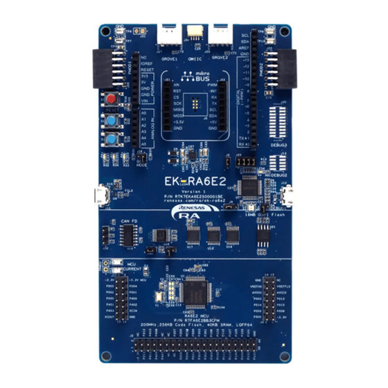
Page 9: Figure 1. Ek-Ra6E2 Board Top Side
Renesas RA Family EK-RA6E2 v1 – User's Manual Grove and Qwiic mikroBus Connectors Connector Arduino Uno Connectors Arduino Uno (Analog and Power) Connectors (Digital) +3.3 V Test Points +5 V Test Points Pmod 1 Pmod 2 Connector Connector Reset Switch... -
Page 10: Assumptions And Advisory Notes
Renesas RA Family EK-RA6E2 v1 – User's Manual Pmod 2 Configuration Grove 2 Configuration Pmod 1 Configuration Debug MCU Power User Button Select Disconnects JTAG GND Detect Disconnect User LED Disconnects RA MCU SWD Disconnect Debug MCU Reset RA MCU SWD... -
Page 11: Kit Contents
Figure 3. EK-RA6E2 Kit Contents 3. Ordering Information • EK-RA6E2 v1 kit orderable part number: RTK7EKA6E2S00001BE Note: The underlined character in the orderable part number represents the kit version. • EK-RA6E2 board dimensions: 80 mm (width) x 140 mm (length) R20UT5177EG0300 Rev. -
Page 12: Hardware Architecture And Default Configuration
Renesas RA Family EK-RA6E2 v1 – User's Manual 4. Hardware Architecture and Default Configuration 4.1 Kit Architecture The EK-RA6E2 board is designed with three sections or areas to help shorten the learning curve of the users and maximize the design and knowledge reuse among similar kits. The contents of these three areas are conceptually standardized among similar kits. -
Page 13: Figure 4. Ek-Ra6E2 Board Functional Area Definitions
Renesas RA Family EK-RA6E2 v1 – User's Manual System Control and Ecosystem Access Area Special Feature Access Area Native Pin Access Area Figure 4. EK-RA6E2 Board Functional Area Definitions R20UT5177EG0300 Rev. 3.00 Page 9 of 31 Mar.01.23... -
Page 14: System Block Diagram
Renesas RA Family EK-RA6E2 v1 – User's Manual 4.2 System Block Diagram Figure 5. EK-RA6E2 Board Block Diagram 4.3 Jumper Settings Two types of jumpers are provided on the EK-RA6E2 board. 1. Copper jumpers (trace-cut type and solder bridge type) 2. -
Page 15: Traditional Pin Header Jumpers
Renesas RA Family EK-RA6E2 v1 – User's Manual A solder-bridge jumper is provided with two isolated pads that may be joined together by one of three methods: • Solder may be applied to both pads to develop a bulge on each and the bulges joined by touching a soldering iron across the two pads. - Page 16 Renesas RA Family EK-RA6E2 v1 – User's Manual Location Circuit Group Default Function Open/Closed User LED Closed Connects P207 to user LED1 User LED Closed Connects P113 to user LED3 Debug MCU Closed Connects the debug MCU power to +3.3 V...
-
Page 17: System Control And Ecosystem Access Area
Renesas RA Family EK-RA6E2 v1 – User's Manual 5. System Control and Ecosystem Access Area The following figure shows the System Control and Ecosystem Access area on the EK-RA6E2 board. Subsequent sections detail the features and functionality provided in this area. -
Page 18: Power
Renesas RA Family EK-RA6E2 v1 – User's Manual 5.1 Power The EK-RA6E2 kit is designed for +5 V operation. An on-board Low Dropout Regulator (LDO) is used to convert the 5 V supply to a 3.3 V supply. The 3.3 V supply is used to power the RA MCU and other peripheral features. -
Page 19: Power Supply Considerations
Open All pins open 5.2.1 Debug On-Board The on-board debug functionality is provided using Renesas RA4M2 Debug MCU and SEGGER J-Link ® firmware. Debug USB micro-B connector (J10) connects the RA4M2 Debug MCU to an external USB Full Speed Host, allowing re-programming and debugging of the target RA MCU firmware. This connection is the default debug mode for the EK-RA6E2 board. -
Page 20: Debug In
Renesas RA Family EK-RA6E2 v1 – User's Manual Debug USB Connector EK-RA6E2 Description Signal/Bus J10-5 Ground A yellow indicator, LED5, shows the visual status of the debug interface. When the EK-RA6E2 board is powered on, and LED5 is blinking, it indicates that the RA4M2 debug MCU is not connected to a programming host. -
Page 21: Debug Out
Renesas RA Family EK-RA6E2 v1 – User's Manual Table 8. JTAG/SWD Connector (J20) JTAG Connector EK-RA6E2 JTAG Pin Name SWD Pin Name Signal/Bus J20-1 Vtref Vtref +3V3 J20-2 SWDIO P108/SWDIO J20-3 J20-4 SWCLK P300/SWCLK J20-5 J20-6 P109 J20-7 J20-8 NC/EXTb... -
Page 22: Ecosystem
Renesas RA Family EK-RA6E2 v1 – User's Manual Table 10. Debug Out Jumper Configuration Location Default Open/Closed Function Open No connection to RA MCU Jumper on pins 2-3 On-board RA MCU is held in RESET Open RA4M2 debug MCU in normal operation mode... -
Page 23: Sparkfun ® Qwiic Connector
Renesas RA Family EK-RA6E2 v1 – User's Manual ® Figure 11. Seeed Grove and SparkFun Qwiic Connectors ® 5.3.2 SparkFun Qwiic Connector ® A SparkFun Qwiic connector is provided at J30. The main MCU acts as a two-wire serial master, and a connected module acts as a two-wire serial slave (data lines are shared with Grove 1 and Grove 2). -
Page 24: Figure 12. Pmod 1 Connector
Renesas RA Family EK-RA6E2 v1 – User's Manual Pmod 1 Connector Default EK-RA6E2 Pmod 1 Configuration J26-6 +3.3 V +5.0 V J26-7 GPIO / INT (slave to master) P105 (IRQ0) J26-8 GPIO / RESET (master to slave) P408 J26-9 GPIO... -
Page 25: Arduino™ Connector
Renesas RA Family EK-RA6E2 v1 – User's Manual Pin 6 Pin 1 Pin 12 Pin 7 Figure 13. Pmod 2 Connector 5.3.4 Arduino™ Connector Near the center of the System Control and Ecosystem Access area is an Arduino Uno R3 compatible connector interface. -
Page 26: Mikroelektronika™ Mikrobus Connector
Renesas RA Family EK-RA6E2 v1 – User's Manual Figure 14. Arduino Uno Connectors 5.3.5 MikroElektronika™ mikroBUS Connector In the center of the System Control and Ecosystem Access area is a mikroBUS compatible connector interface. This interface is compliant with mikroBUS Standard Specifications revision 2.00. -
Page 27: Connectivity
Renesas RA Family EK-RA6E2 v1 – User's Manual 5.4 Connectivity 5.4.1 USB Full Speed The USB micro-AB connection jack (J11) connects the RA MCU USB Full Speed interface to an external USB interface, allowing communications for testing and use of the RA MCU firmware. This connection can be configured as a USB device. -
Page 28: User And Reset Switches
Renesas RA Family EK-RA6E2 v1 – User's Manual LED5 Yellow Debug LED J-Link OB MCU The user LEDs may be isolated from the main MCU so the associated ports can be used for other purposes. To separate LED1 from P207, trace-cut jumper E27 must be open. To separate LED2 from P400, trace-cut jumper E26 must be open. -
Page 29: Mcu Boot Mode
Renesas RA Family EK-RA6E2 v1 – User's Manual 5.5.3 MCU Boot Mode A two-pin header (J16) is provided to select the Boot mode (P201) of the RA MCU. For normal operation, or Single-Chip mode, leave J16 open. To enter SCI Boot mode or USB Boot mode, place a jumper on J16. -
Page 30: Can Bus
Renesas RA Family EK-RA6E2 v1 – User's Manual Figure 22. Quad-SPI Flash Note: Some of the QSPI pins on the RA device conflict with the I3C lines. Use of QSPI can be enabled by setting J35 to closed. When QSPI is in use, the board will automatically switch to using I C lines. -
Page 31: Mcu Native Pin Access Area
Renesas RA Family EK-RA6E2 v1 – User's Manual 7. MCU Native Pin Access Area Figure 24. Native Pin Access Area 7.1 Breakout Pin Headers The EK-RA6E2 board pin headers, J1, J2, and J3, provide access to all RA MCU interface signals, and to voltages for all RA MCU power ports. -
Page 32: Mcu And Usb Current Measurement
Renesas RA Family EK-RA6E2 v1 – User's Manual 7.2 MCU and USB Current Measurement Included in the Native Pin Access area are current measurement resistors and test points to measure the MCU USB controller current and the MCU core power current. -
Page 33: Certifications
Renesas RA Family EK-RA6E2 v1 – User's Manual 8. Certifications The EK-RA6E2 v1 kit meets the following certifications/standards. See page 4 of this user’s manual for the disclaimer and precautions. 8.1 EMC/EMI Standards • FCC Notice (Class A) This device complies with part 15 of the FCC Rules. Operation is subject to the following two conditions: (1) This device may not cause harmful interference, and (2) this device must accept any interference received, including interference that may cause undesired operation. -
Page 34: Design And Manufacturing Information
Renesas RA Family EK-RA6E2 v1 – User's Manual 9. Design and Manufacturing Information The design and manufacturing information for the EK-RA6E2 v1 kit is available in the “EK-RA6E2 v1 Design Package” available on renesas.com/ra/ek-ra6e2. • Design package file name: ek-ra6e2-v1-designpackage.zip •... -
Page 35: Revision History
Renesas RA Family EK-RA6E2 v1 – User's Manual Revision History Description Rev. Date Page Summary 1.00 Jul.13.22 — Initial release 2.00 Feb.14.23 — Updated for ES release 3.00 Mar.01.23 — Updated for MP release R20UT5177EG0300 Rev. 3.00 Page 31 of 31... - Page 36 EK-RA6E2 v1 – User’s Manual Publication Date: Mar.01.23 Published by: Renesas Electronics Corporation...
- Page 37 EK-RA6E2 v1 – User’s Manual R20UT5177EG0300...
Need help?
Do you have a question about the EK-RA6E2 v1 and is the answer not in the manual?
Questions and answers