Table of Contents
Advertisement
Quick Links
High Power PolyPhase
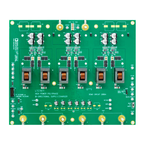
DESCRIPTION
Demonstration circuit 2886A is a high power, high effi-
ciency six-phase bidirectional converter featuring the
LTC
7871
and LTC7060. The terminals labeled V
®
and V
are either inputs or outputs depending on the
LOW
direction of power flow. When the switch at SW1 is in the
BUCK position, V
provides a 14V output and V
LOW
the input with a range of 30V to 70V. When the switch
is in the BOOST position, V
and V
is the input with a range of 10V to 14V. The
LOW
maximum V
current is 180A in both directions. The
LOW
maximum output power is 2.5kW when operating as a
buck within the input voltage range. When operating as
a boost, the maximum output power is 2.4kW when the
input voltage is 14V. External airflow is required when
operating at maximum power. The MOSFETs in each
phase are driven by the LTC7060 half bridge driver. Each
LTC7060 gate driver is placed next to the MOSFETs and
receives a PWM signal from the LTC7871.
The inductor current for each phase is sensed with a low
1mΩ sense resistor using a highly accurate AC/DC cur-
rent sensing architecture with low power dissipation. The
LTC7871's constant-current loop provides a DC current
limit for the current flowing in or out of the V
depending on the state of the BUCK pin. This current can
be programmed with the SETCUR pin and monitored with
the IMON pin.
®
HIGH
HIGH
provides a 48V output
HIGH
terminal
LOW
DEMO MANUAL DC2886A
Bidirectional Supply/Charger
The DC2886A provides a SPI compatible serial port. With
a DC2026C (Linduino
software on a host computer, the user can:
• Margin the regulated V
• Margin the DC current limit up or down with the
is
SETCUR pin.
• Adjust the frequency spread and modulation rate of
the spread spectrum circuit, when spread spectrum
is enabled.
• Monitor the operational status and faults of
the LTC7871.
Additional features of the DC2886A include:
• Pin selectable light load operating modes
– Buck: FCM, pulse-skipping and Burst Mode
Operation
– Boost: FCM and pulse-skipping
• SYNC and CLKOUT pins
• Optional jumper to enable spread spectrum modulation
• RUN, FAULT, PGOOD and PWNEN pins
• BUCK pin to externally control the direction of
power flow
• Footprint for an optional heatsink
Design files for this circuit board are
All registered trademarks and trademarks are the property of their respective owners.
LTC7871/LTC7060
One) demo board and QuikEval™
®
or V
up or down.
LOW
HIGH
available.
®
Rev. 0
1
Advertisement
Table of Contents

Related Manuals for Linear ADI Power LTC7871


Summary of Contents for Linear ADI Power LTC7871
- Page 1 DEMO MANUAL DC2886A LTC7871/LTC7060 High Power PolyPhase Bidirectional Supply/Charger ® DESCRIPTION Demonstration circuit 2886A is a high power, high effi- The DC2886A provides a SPI compatible serial port. With ciency six-phase bidirectional converter featuring the a DC2026C (Linduino One) demo board and QuikEval™ ®...
-
Page 2: Performance Summary
DEMO MANUAL DC2886A BOARD PHOTO PERFORMANCE SUMMARY Specifications are at T = 25°C SYMBOL PARAMETER CONDITIONS UNITS Buck Mode Supply Range HIGH Output Voltage 13.6 14.0 14.4 LOW(MAX) Operating Frequency SWITCH Efficiency = 48V 97.5 HIGH = 180A 400LFM Airflow Boost Mode Supply Range Output Voltage... -
Page 3: Quick Start Procedure
DEMO MANUAL DC2886A QUICK START PROCEDURE Instructions for operating the DC2886A are below. 4. Turn on the V supply. With no load, slowly increase HIGH the V supply until V reaches 30V. At this point, HIGH HIGH Constant-Voltage (CV) Buck Mode 14V should appear on V . - Page 4 DEMO MANUAL DC2886A QUICK START PROCEDURE Constant-Voltage (CV) Boost Mode 5. Next, increase V to 14V. Recheck the regulation. 1. Refer to the connection diagram in Figure 2. 6. Apply load up to 51A across V . Recheck HIGH the regulation. 2. Place SW1 in the BOOST position. 7.
- Page 5 DEMO MANUAL DC2886A QUICK START PROCEDURE Constant-Current (CC) Mode 3. Connect a bench voltage source to the SETCUR pin as shown in Figure 4. This could be either a DC voltage The DC2886A can operate as a constant-current source or the output of a pulse generator. when operating either as a buck or a boost.
- Page 6 DEMO MANUAL DC2886A QUICK START PROCEDURE PROBE HIGH ~1mF ~10mF E-LOAD E-LOAD HIGH HIGH SUPPLY SUPPLY CV MODE CV MODE DC2886A PULSE BUCK SETCUR GENERATOR – SETCUR dc2886a F05 Figure 5. Typical Setup for the Buck/Boost Transition Test External Bulk Capacitance Thermal Considerations Additional bulk capacitance may be required across the With full continuous load on the output in either direc-...
- Page 7 DEMO MANUAL DC2886A QUICK START PROCEDURE SPI Interface 5. Refer to the demo manual of the DC2026C for further details. To control or monitor the DC2886A from QuikEval on a host computer, follow these steps: 6. Apply a voltage within the specified input range to either V or V depending on the direction of...
-
Page 8: Typical Performance Characteristics
DEMO MANUAL DC2886A QUICK START PROCEDURE b. QuikEval can margin V and the DC I margin the V or DC I current limit HIGH HIGH current limit up or down by writing to the register to a given value. To use this tool, enter the values which controls the current source digital to ana- for the feedback divider or SETCUR resistor and log converter (IDAC) for the VFB... - Page 9 DEMO MANUAL DC2886A TYPICAL PERFORMANCE CHARACTERISTICS HIGH HIGH dc2886a F14 dc2886a F15 AIRFLOW AIRFLOW Figure 14. Thermal Image While Operating as a BUCK, Figure 15. Thermal Image While Operating as a BOOST, = 48V, V = 14V, Load = 180A, Airflow = 400LFM, = 14V, V = 48V, Load = 51A, Airflow = 400LFM, HIGH...
- Page 10 DEMO MANUAL DC2886A PARTS LIST ITEM QTY REFERENCE PART DESCRIPTION MANUFACTURER/PART NUMBER Required Circuit Components RES., 10k , 5%, 1/10W, 0603 SAMSUNG, RC1608J103CS YAGEO, RC0603JR-0710KL RES., 1k , 5%, 1/10W, 0603 SAMSUNG, RC1608J102CS YAGEO, RC0603JR-071KL R67, R400, R403, R406, R409, R412 RES., 1Ω, 1%, 1/10W, 0603 YAGEO, RC0603FR-071RL RES., 48.7k , 1%, 1/10W, 0603, AEC-Q200...
-
Page 11: Parts List
DEMO MANUAL DC2886A PARTS LIST ITEM QTY REFERENCE PART DESCRIPTION MANUFACTURER/PART NUMBER R425, R438 RES., 45.3k , 1%, 1/10W, 0603, AEC-Q200 PANASONIC, ERJ3EKF4532V VISHAY, CRCW060345K3FKEA R38, R41, R42, R50, R94, R112 RES., 1.69k , 1%, 1/10W, 0603, AEC-Q200 NIC, NRC06F1691TRF PANASONIC, ERJ3EKF1691 VISHAY, CRCW06031K69FKEA RES., 130k , 1%, 1/8W, 0805... - Page 12 DEMO MANUAL DC2886A PARTS LIST ITEM QTY REFERENCE PART DESCRIPTION MANUFACTURER/PART NUMBER Q5, Q6, Q7, Q8, Q18, Q19, Q21, XSTR., MOSFET, N-CH, 80V, 95A, PG-TDSON-8 INFINEON, BSC052N08NS5, Q23, Q35, Q36, Q38, Q41 BSC052N08NS5ATMA1 U1, U2, U3, U4, U5, U6 IC, DC/DC CONVERTER, MSE-12 ANALOG DEVICES, LTC7060EMSE#PBF , LTC7060EMSE#TRPBF IC, HIGH POWER POLY-PHASE, BIDIRECTIONAL...
-
Page 13: Schematic Diagram
DEMO MANUAL DC2886A SCHEMATIC DIAGRAM Rev. 0... - Page 14 DEMO MANUAL DC2886A SCHEMATIC DIAGRAM Rev. 0...
- Page 15 DEMO MANUAL DC2886A SCHEMATIC DIAGRAM Rev. 0 Information furnished by Analog Devices is believed to be accurate and reliable. However, no responsibility is assumed by Analog Devices for its use, nor for any infringements of patents or other rights of third parties that may result from its use. Specifications subject to change without notice.
- Page 16 DEMO MANUAL DC2886A ESD Caution ESD (electrostatic discharge) sensitive device. Charged devices and circuit boards can discharge without detection. Although this product features patented or proprietary protection circuitry, damage may occur on devices subjected to high energy ESD. Therefore, proper ESD precautions should be taken to avoid performance degradation or loss of functionality. Legal Terms and Conditions By using the evaluation board discussed herein (together with any tools, components documentation or support materials, the “Evaluation Board”), you are agreeing to be bound by the terms and conditions set forth below (“Agreement”) unless you have purchased the Evaluation Board, in which case the Analog Devices Standard Terms and Conditions of Sale shall govern.
Need help?
Do you have a question about the ADI Power LTC7871 and is the answer not in the manual?
Questions and answers