Table of Contents
Advertisement
Quick Links
Advertisement
Table of Contents

Subscribe to Our Youtube Channel
Related Manuals for Symphonic STL20D5


Summary of Contents for Symphonic STL20D5
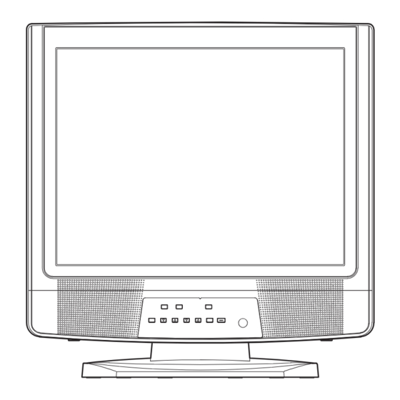
- Page 1 SERVICE MANUAL 20″ LCD TV/DVD STL20D5...
- Page 2 IMPORTANT SAFETY NOTICE Proper service and repair is important to the safe, reliable operation of all Funai Equipment. The service procedures recommended by Funai and described in this service manual are effective methods of performing service operations. Some of these service special tools should be used when and as recommended.
-
Page 3: Table Of Contents
TABLE OF CONTENTS Specifications ................1-1 Laser Beam Safety Precautions . -
Page 4: Specifications
SPECIFICATIONS < LCD TV Section > < TUNER > ANT. Input ---------------------- 75 ohm Unbal., F type Reference Level--------------- 20 Vp-p (LCD Green Cathode) Test Input Signal -------------- 400 Hz 30% modulation Description Condition Unit Nominal Limit Picture 45.75 1. Intermediate Freq. Sound 41.25 2. - Page 5 <DVD Section> ITEM CONDITIONS UNIT NOMINAL LIMIT 1. Coaxial Digital Out 75 ohm load mVpp ± 100 NOTES: 1. All Items are measured without pre-emphasis unless otherwise specified. 2. Power supply : AC120 V 60 Hz ° 3. Ambient temperature: +25 L3250SP...
-
Page 6: Laser Beam Safety Precautions
LASER BEAM SAFETY PRECAUTIONS This DVD player uses a pickup that emits a laser beam. Do not look directly at the laser beam coming from the pickup or allow it to strike against your skin. The laser beam is emitted from the location shown in the figure. When checking the laser diode, be sure to keep your eyes at least 30 cm away from the pickup lens when the diode is turned on. -
Page 7: Important Safety Precautions
IMPORTANT SAFETY PRECAUTIONS Prior to shipment from the factory, our products are strictly inspected for recognized product safety and electrical codes of the countries in which they are to be sold. However, in order to maintain such compliance, it is equally important to implement the following precautions when a set is being serviced. - Page 8 3. Design Alteration Warning - Do not alter or add 7. Product Safety Notice - Some electrical and to the mechanical or electrical design of this TV mechanical parts have special safety-related receiver. Design alterations and additions, characteristics which are often not evident from including, but not limited to circuit modifications visual inspection, nor can the protection they give and the addition of items such as auxiliary audio...
- Page 9 Precautions during Servicing A. Parts identified by the # symbol are critical for L. When connecting or disconnecting the internal safety. connectors, first, disconnect the AC plug from the Replace only with part number specified. AC supply outlet. B. In addition to safety, other parts and assemblies M.
- Page 10 Safety Check after Servicing Examine the area surrounding the repaired location for damage or deterioration. Observe that screws, parts and wires have been returned to original positions. Afterwards, perform the following tests and confirm the specified values in order to verify compliance with safety standards. 1.
-
Page 11: Standard Notes For Servicing
STANDARD NOTES FOR SERVICING Circuit Board Indications Pb (Lead) Free Solder 1. The output pin of the 3 pin Regulator ICs is Pb free mark will be found on PCBs which use Pb indicated as shown. free solder. (Refer to figure.) For PCBs with Pb free mark, be sure to use Pb free solder. - Page 12 around the flat pack-IC to protect other parts from With Soldering Iron: damage. (Fig. S-1-2) 1. Using desoldering braid, remove the solder from 3. The flat pack-IC on the CBA is affixed with glue, so all pins of the flat pack-IC. When you use solder be careful not to break or damage the foil of each flux which is applied to all pins of the flat pack-IC, pin or the solder lands under the IC when...
- Page 13 2. Installation With Iron Wire: 1. Using desoldering braid, remove the solder from 1. Using desoldering braid, remove the solder from all pins of the flat pack-IC. When you use solder the foil of each pin of the flat pack-IC on the CBA flux which is applied to all pins of the flat pack-IC, so you can install a replacement flat pack-IC more you can remove it easily.
- Page 14 Instructions for Handling Semi- conductors Electrostatic breakdown of the semi-conductors may occur due to a potential difference caused by electrostatic charge during unpacking or repair work. 1. Ground for Human Body Be sure to wear a grounding band (1 MΩ) that is properly grounded to remove any static electricity that may be charged on the body.
-
Page 15: Cabinet Disassembly Instructions
CABINET DISASSEMBLY INSTRUCTIONS 1. Disassembly Flowchart Removal Step/ This flowchart indicates the disassembly steps for the Remove/*Unhook/ Loc. Part Fig. Unlock/Release/ cabinet parts, and the CBA in order to gain access to Note Unplug/Unclamp/ item(s) to be serviced. When reassembling, follow the Desolder steps in reverse order. - Page 16 Reference Notes 1. CAUTION 1: Electrostatic breakdown of the laser diode in the optical system block may occur as a potential difference caused by electrostatic charge accumulated on cloth, human body etc., during unpacking or repair work. To avoid damage of pickup follow next procedures. 1) Short the three short lands of FPC cable with solder before removing the FFC cable (CN201) from it.
- Page 17 (S-1) (S-1) (S-2) (S-1) (S-1) [1] Rear Cabinet (S-3) (S-1) Tilt Stand Assembly Fig. D1 L3250DC...
- Page 18 [6] DVD Holder(R) (S-9) [5] DVD Mechanism [2] Jack Holder (S-4) (S-9) (S-10) (S-8) [7] DVD Holder(L) (S-5) (S-7B) (S-10) (S-4) (S-7A) [4] Loader (S-6) PCB Holder [3] DVD Main CBA Unit Remove four screws A, then short the three short lands by soldering as shown in View for A. Screws A Chassis Cover Pin A...
- Page 19 (S-12) (S-11) (S-11) (S-12) [9] Inverter CBA (S-13) [10] Tilt Stand (S-14) (S-11) Holder (S-11) [8] Main CBA Fig. D3 L3250DC...
- Page 20 [16] Front Cabinet [14] Speaker(R) (S-18) (S-15) (S-15) [12] Function CBA (S-16) (S-15) (S-15) (S-16) (S-17) [13] IR Sensor CBA (S-15) [11] LCD Main CBA & Liquid Crystal Panel Unit (S-19) (S-15) [15] Speaker(L) Fig. D4 L3250DC...
- Page 21 TV Cable Wiring Diagram To Liquid Crystal Function CBA To DVD Mechanism Panel CLN104 Main CBA IR Sensor CBA CN104 CN311 CLN105 CN312 CN201 CN105 CN301 CN1751 CN801 CN111 CN601 CN1761 CN401 CN112 CN102B CN103B DVD Main CBA Unit CN101B Main CBA CN113 CN1701...
- Page 22 3. How to Eject Manually 1. Remove the Rear Cabinet. 2. To remove the Loader PCB Holder with the DVD Main CBA Unit, remove three screws (S-7) in Fig. D2. Do not disconnect connectors. 3. To remove the Chassis Cover, remove 4 screws A as shown in Fig.
-
Page 23: Electrical Adjustment Instructions
ELECTRICAL ADJUSTMENT INSTRUCTIONS General Note: “CBA” is abbreviation for How to set up the service mode: “Circuit Board Assembly.” Service mode: Note: Electrical adjustments are required after 1. Use the service remote control unit. replacing circuit components and certain mechanical parts. It is important to perform 2. - Page 24 3. If Flicker Adjustment is not fit, the screen becomes Button the following. [Use the attached Data Item remote control unit. Value (not service remote control unit)] VCOM D2-BRT D2-CNT D2-CLR-R [MENU] → [5] D2-CLR-B D2-TNT D2-SHR D3-BRT D3-CNT FLASH (Go and Off) D3-CLR-R [MENU] →...
- Page 25 The following adjustment normally are not 5. [RF/VIDEO1] attempted in the field. Only when replacing the When “x” value and “y” value are not within LCD Panel then adjust as a preparation. specification, adjust “DB (C/D1)” or “DR (C/D1)”. Refer to “1. Initial Setting.” 3.
-
Page 26: How To Initialize The Lcd Tv/Dvd
HOW TO INITIALIZE THE LCD TV/DVD To put the program back at the factory-default, initialize the LCD TV/DVD as the following procedure. < DVD Section > < LCD TV Section > 1. Press [1], [2], [3], [4], and [DISPLAY] buttons on the 1. -
Page 27: Firmware Renewal Mode
FIRMWARE RENEWAL MODE 1. Turn the power on and press [EJECT] button on the 5. After programming is finished, the disc will be remote control unit to put the LCD TV/DVD into ejected automatically. Fig. e appears on the screen DVD mode. -
Page 28: Block Diagrams
BLOCK DIAGRAMS < LCD TV SECTION > System Control Block Diagram L3251BLS... - Page 29 IF/Video Block Diagram L3251BLIF...
- Page 30 Audio Block Diagram L3251BLA...
- Page 31 LCD Block Diagram L3251BLLCD...
- Page 32 Power Supply Block Diagram L3251BLP...
- Page 33 LCD Backlight Block Diagram L3251BLLB...
- Page 34 BLOCK DIAGRAMS < DVD SECTION > System Control / Servo Block Diagram L3251BLSD...
- Page 35 Digital Signal Process Block Diagram L3251BLD...
-
Page 36: Schematic Diagrams / Cba's And Test Points
SCHEMATIC DIAGRAMS / CBA'S AND TEST POINTS Standard Notes Many electrical and mechanical parts in this chassis have special characteristics. These characteristics often pass unnoticed and the protection afforded by them cannot necessarily be obtained by using replacement components rated for higher voltage, wattage, etc. Replacement parts that have these special safety characteristics are identified in this manual and its supplements;... - Page 37 LIST OF CAUTION, NOTES, AND SYMBOLS USED IN THE SCHEMATIC DIAGRAMS ON THE FOLLOWING PAGES: 1. CAUTION: CAUTION: FOR CONTINUED PROTECTION AGAINST RISK OF FIRE, REPLACE ONLY WITH SAME TYPE_A,_V FUSE. ATTENTION: UTILISER UN FUSIBLE DE RECHANGE DE MÊME TYPE DE_A,_V. 2.
- Page 38 Main 1/4 Schematic Diagram MAIN 1/4 Ref No. Position IC531 IC533 IC671 IC672 TRANSISTORS Q501 Q502 Q503 Q505 Q509 Q510 Q511 Q512 Q513 Q531 Q633 CONNECTORS CN101A CN102A CN411 L3251SCM1 10-3...
- Page 39 Main 2/4 Schematic Diagram MAIN 2/4 Ref No. Position IC31 IC851 IC852 TRANSISTOR CONNECTOR CN113 L3251SCM2 10-4...
- Page 40 Main 3/4 Schematic Diagram MAIN 3/4 Ref No. Position IC781 IC801 TRANSISTORS Q701 Q702 Q703 Q704 Q705 Q706 Q707 Q708 Q802 Q803 Q804 Q1701 CONNECTORS CN103A CN801 CN802 CN1701 TEST POINTS TP1801 TP1802 TP1803 TP1804 TP1805 TP1806 L3251SCM3 10-5...
- Page 41 Main 4/4 Schematic Diagram NOTE: CAUTION ! The voltage for parts in hot circuit is measured using Fixed voltage (or Auto voltage selectable) power supply circuit is used in this unit. CAUTION ! : For continued protection against risk of fire, hot GND as a common terminal.
- Page 42 Inverter Schematic Diagram INVERTER Ref No. Position IC401 IC402 TRANSISTORS Q403 Q411 Q412 Q421 Q426 Q433 Q451 Q452 Q454 Q455 Q461 Q462 Q491 Q492 CONNECTORS CLN411 CN450 CN460 CN490 L3251SCI 10-7...
- Page 43 Function Schematic Diagram L3251SCF 10-8...
- Page 44 IR Sensor Schematic Diagram L3251SCIR 10-9...
- Page 45 LCD Main 1/2 Schematic Diagram LCD MAIN 1/2 Ref No. Position IC333 TRANSISTOR Q301 CONNECTORS CN102B CN104 CN105 CN311 L3251SCL1 10-10...
- Page 46 LCD Main 2/2 Schematic Diagram LCD MAIN 2/2 Ref No. Position IC151 IC171 IC191 IC192 IC193 IC201 TRANSISTORS Q131 Q201 CONNECTORS CN101B CN103B CN312 CN1751 CN1761 L3251SCL2 10-11...
- Page 47 DVD Main 1/3 Schematic Diagram DVD MAIN 1/3 1 NOTE: Ref No. Position Either IC461 or IC462 is used for DVD MAIN CBA UNIT. IC201 IC202 IC301 IC461 IC462 TRANSISTORS Q251 Q252 Q253 Q254 Q801 Q802 Q804 CONNECTORS CN201 CN301 CN401 CN801 L3251SCD1...
- Page 48 DVD Main 2/3 Schematic Diagram L3251SCD2 10-13...
- Page 49 IC101 Voltage Chart ~ : Voltage is not consistent ----- : Not used Unit : Volts PIN.NO PLAY STOP PIN.NO PLAY STOP PIN.NO PLAY STOP PIN.NO PLAY STOP PIN.NO PLAY STOP PIN.NO PLAY STOP PIN.NO PLAY STOP PIN.NO PLAY STOP ----- ----- -----...
- Page 50 DVD Main 3/3 Schematic Diagram DVD MAIN 3/3 Ref No. Position IC103 IC501 IC502 IC601 CONNECTOR CN601 L3251SCD3 10-15...
- Page 51 Main CBA Top View CAUTION ! Because a hot chassis ground is present in the power Fixed voltage (or Auto voltage selectable) power supply circuit is used in this unit. supply circuit, an isolation transformer must be used. CAUTION ! : For continued protection against risk of fire, If Main Fuse (F601) is blown , check to see that all components in the power supply Also, in order to have the ability to increase the input...
- Page 52 Main CBA Bottom View CAUTION ! Because a hot chassis ground is present in the power Fixed voltage (or Auto voltage selectable) power supply circuit is used in this unit. supply circuit, an isolation transformer must be used. CAUTION ! : For continued protection against risk of fire, If Main Fuse (F601) is blown , check to see that all components in the power supply Also, in order to have the ability to increase the input...
- Page 53 Inveretr CBA Top View INVERTER Ref No. Position IC401 IC402 TRANSISTORS Q403 Q411 Q412 Q421 Q426 Q433 Q451 Q452 Q454 Q455 Q461 Q462 Q491 Q492 CONNECTORS CLN411 CN450 CN460 CN490 Inverter CBA Bottom View BL3100F01022-1 10-18...
- Page 54 Function CBA Top View IR Sensor CBA Top & Bottom View BL3100F01022-2 BL3150F01012-3 Function CBA Bottom View BL3100F01022-2 10-19...
-
Page 55: Waveforms
WAVEFORMS < LCD TV SECTION > WF1 ~ WF12 = Waveforms to be observed at Waveform check points. (Shown in Schematic Diagram.) Input: NTSC Color Bar Signal (with 1kHz Audio Signal) CLKH STH1 S-VIDEO-C 1DIV: 1.0V 10 s 1DIV: 1.0V 10 s 1DIV: 200mV 20 s R392 R394... - Page 56 WAVEFORMS < DVD SECTION > DVD-AUDIO(R) DVD-AUDIO(R) 0.5ms 0.5ms DVD-Y DVD-Y 0.1V 0.1V 20µs WF13 WF16 Pin 1 of CN1701 Pin 8 of CN1701 DVD-C DVD-C 0.1V 0.1V 20µs SPDIF SPDIF 0.1µs WF14 WF17 Pin 3 of CN1701 Pin 11 of CN1701 NOTE: Input CD: 1kHz PLAY...
-
Page 57: Wiring Diagram
WIRING DIAGRAM < LCD TV SECTION > L3251WI 12-1... - Page 58 WIRING DIAGRAM < DVD SECTION > P-ON+5V 20 CD/DVD 19 D 18 DVD-Y A 17 C 16 DVD-C B 15 E 14 VREF 13 DVD-AUDIO(L) F 12 DVD-MUTE GND 11 DVD-AUDIO(R) CD-LD 10 DVD-AUDIO+5V 16 GND(LD) 9 DVD-AUDIO+5V 17 DVD-LD 8 SPDIF PD-MONI 7 GND(DVD-PD) 6...
-
Page 59: System Control Timing Charts
SYSTEM CONTROL TIMING CHARTS Disc In ~ Play/Play ~ Disc Out Disc Disc Disc Disc Play Rotation Stop 3.3V Disc IN (TL221) 1.65V Sled Drive (TP303) 1.65V Disc Drive (TP301) 1.65V Focus Drive (TP304) Tracking Drive 1.65V (TP302) 13-1 L3150TI... -
Page 60: Lead Identifications
LEAD IDENTIFICATIONS 2SC2785(F) 2SA1175(F) KIA7805API 2SC2120-O(TE2 F T) BA1F4M-T 2SC2120-Y(TE2 F T) KTC3205-Y-AT/P 2SD400(F) 1: IN 2: GND 3: OUT 1 2 3 E C B E C B PS2501-1L AN5832SA-E1V TC4053BF(EL.N) AN17812A TC4052BF(EL) 1: A 2: K 3: E 4: C PQ070XF01SZH 2SK3869(Q) -
Page 61: Exploded Views
EXPLODED VIEWS Cabinet LCD Main CBA & Liquid Crystal Panel Unit CLN802 SP802 Function CBA IR Sensor CBA Inverter CBA CLN801 CL1651 SP801 See Electrical Parts List for parts with this mark. Main CBA DVD Main CBA Unit AC601 CL1701 CL1761 15-1 L3250CEX... - Page 62 Packing Some Ref. Numbers are not in sequence. Tape Tape Packing Tape Packing Tape Packing Tape 15-2 L3250PEX...
-
Page 63: Mechanical Parts List
MECHANICAL PARTS LIST PRODUCT SAFETY NOTE: Products marked with a Ref. No. Description # have special characteristics important to safety. PACKING Before replacing any of these components, read CARTON L3251UB 1EM422165 carefully the product safety notice in this service STYROFOAM TOP L3250UA 1EM020208 manual. -
Page 64: Electrical Parts List
ELECTRICAL PARTS LIST PRODUCT SAFETY NOTE: Products marked with a Ref. No. Description Part No. # have special characteristics important to safety. CHIP CERAMIC CAP .(1608) CH J 47pF/50V CHD1JJ3CH470 Before replacing any of these components, read ELECTROLYTIC CAP . 1µF/50V M H7 CE1JMASSL010 carefully the product safety notice in this service CHIP CERAMIC CAP .(1608) CH J 47pF/50V... - Page 65 Ref. No. Description Part No. Ref. No. Description Part No. C702 CHIP CERAMIC CAP .(1608) B K 0.01µF/50V CHD1JK30B103 C864 CHIP CERAMIC CAP .(1608) B K 0.022µF/50V CHD1JK30B223 C703 ELECTROLYTIC CAP . 47µF/16V M H7 CE1CMAVSL470 C865 CHIP CERAMIC CAP .(1608) B K 0.1µF/50V CHD1JK30B104 C704 ELECTROLYTIC CAP .
- Page 66 Ref. No. Description Part No. Ref. No. Description Part No. D613 SWITCHING DIODE 1SS133(T-77) QDTZ001SS133 IC781 IC TC4053BF(EL.N) QSZBA0TTS131 D615 SWITCHING DIODE 1SS133(T-77) QDTZ001SS133 IC801 IC AN17812A QSZBA0SMS017 D616# ZENER DIODE MTZJT-7733B QDTB00MTZJ33 IC851 IC MTS DECORDER AN5832SA-E1V QSZBA0TMS003 D620 SWITCHING DIODE 1SS133(T-77) QDTZ001SS133 IC852...
- Page 67 Ref. No. Description Part No. Ref. No. Description Part No. CHIP RES.(1608) 1/10W J 15k Ω CHIP RES.(1608) 1/10W F 2.7k Ω RRXAJR5Z0153 R652# RRXAFR5H2701 CHIP RES.(1608) 1/10W J 220 Ω CHIP RES.(1608) 1/10W F 2.7k Ω RRXAJR5Z0221 R653# RRXAFR5H2701 CHIP RES.(1608) 1/10W J 1k Ω...
- Page 68 Ref. No. Description Part No. Ref. No. Description Part No. CHIP RES.(1608) 1/10W J 10k Ω CHIP RES.(1608) 1/10W F 56k Ω R787 RRXAJR5Z0103 R1665 RRXAFR5H5602 CARBON RES. 1/4W J 10k Ω R788 RCX4JATZ0103 R1666 PCB JUMPER D0.6-P5.0 JW5.0T CHIP RES.(1608) 1/10W J 10k Ω CHIP RES.(1608) 1/10W J 47k Ω...
- Page 69 Ref. No. Description Part No. Ref. No. Description Part No. CHIP RES.(1608) 1/10W 0 Ω JS21 RRXAZR5Z0000 C422 CHIP CERAMIC CAP .(1608) B K 0.1µF/50V CHD1JK30B104 JS524 PCB JUMPER D0.6-P5.0 JW5.0T C423 ELECTROLYTIC CAP . 47µF/35V M CA1G470SP096 JS530 PCB JUMPER D0.6-P15.0 JW15.0T C425 CHIP CERAMIC CAP .(1608) B K 0.1µF/50V...
- Page 70 Ref. No. Description Part No. Ref. No. Description Part No. CHIP RES.(1608) 1/10W J 10k Ω D457 SWITCHING DIODE 1SS133(T-77) QDTZ001SS133 R437 RRXAJR5Z0103 CHIP RES.(1608) 1/10W 0 Ω D460 SWITCHING DIODE 1SS400 QD1Z001SS400 R438 RRXAZR5Z0000 CHIP RES.(1608) 1/10W 0 Ω D461 SWITCHING DIODE 1SS133(T-77) QDTZ001SS133...
- Page 71 Ref. No. Description Part No. CHIP RES.(1608) 1/10W J 2.7k Ω RRXAJR5Z0272 CHIP RES.(1608) 1/10W J 4.7k Ω RRXAJR5Z0472 CHIP RES.(1608) 1/10W J 6.8k Ω RRXAJR5Z0682 CHIP RES.(1608) 1/10W J 10k Ω RRXAJR5Z0103 CHIP RES.(1608) 1/10W J 47 Ω RRXAJR5Z0470 CHIP RES.(1608) 1/10W J 1.5k Ω...
- Page 72 STL20D5 L3251UB 2005-10-13...
Need help?
Do you have a question about the STL20D5 and is the answer not in the manual?
Questions and answers