Table of Contents
Advertisement
Quick Links
Advertisement
Table of Contents

Related Manuals for Supero SUPER P3TSSA

Summary of Contents for Supero SUPER P3TSSA
- Page 1 ® UPER SUPER P3TSSA SUPER P3TSSR SUPER P3TSSE USER’S MANUAL Revision 1.0c...
- Page 2 The State of California, County of Santa Clara shall be the exclusive venue for the resolution of any such disputes. Supermicro's total liability for all claims will not exceed the price paid for the hardware product. Unless you request and receive written permission from SUPER MICRO COMPUTER, you may not copy any part of this document.
-
Page 3: About This Manual
Celeron processors at front side bus speeds of 100 and 66 MHz. Please refer to the support section of our web site (http://www.supermicro.com/ TechSupport.htm) for a complete listing of supported processors. Intel FCPGA processors are housed in a 370-pin package. -
Page 4: Table Of Contents
SUPER P3TSSA Image ... 1-3 SUPER P3TSSR Image ... 1-4 SUPER P3TSSE Image ... 1-5 SUPER P3TSSA Layout ... 1-6 SUPER P3TSSA Quick Reference ... 1-7 SUPER P3TSSR Layout ... 1-8 SUPER P3TSSR Quick Reference ... 1-9 SUPER P3TSSE Layout ... 1-10 SUPER P3TSSE Quick Reference ... - Page 5 Keylock/Power LED ... 2-8 Speaker ... 2-9 ATX PS/2 Keyboard/Mouse Ports ... 2-9 Universal Serial Bus ... 2-9 Serial Ports ... 2-10 Wake-On-LAN ... 2-10 CD Headers ... 2-10 Fan Headers ... 2-11 Chassis Intrusion Header ... 2-11 Overheat LED ... 2-11 Speaker Header ...
- Page 6 UPER P3TSSA/P3TSSR/P3TSSE User’s Manual Chapter 4: BIOS Introduction ... 4-1 BIOS Features ... 4-2 Running Setup ... 4-2 Advanced Chipset Setup ... 4-4 Chipset Setup ... 4-16 PCI PnP Setup ... 4-24 Power Setup ... 4-28 Boot Setup ... 4-34 Security Setup ...
-
Page 7: Chapter 1 Introduction
One (1) floppy ribbon cable for (1) 5.25-inch floppy and (2) 3.5-inch floppy drives One (1) serial COM 2 cable (retail box only) One (1) Supermicro CD or diskettes containing drivers and utilities One (1) User's/BIOS Manual SCSI Accessories (P3TSSR only):... -
Page 8: Contacting Supermicro
UPER P3TSSA/P3TSSR/P3TSSE User's Manual Contacting Supermicro Headquarters Address: Super Micro Computer, Inc. 980 Rock Ave. San Jose, CA 95131 U.S.A. Tel: +1 (408) 503-8000 Fax: +1 (408) 503-8008 Email: marketing@supermicro.com (General Information) support@supermicro.com (Technical Support) Web Site: www.supermicro.com Europe Address: Super Micro Computer B.V. -
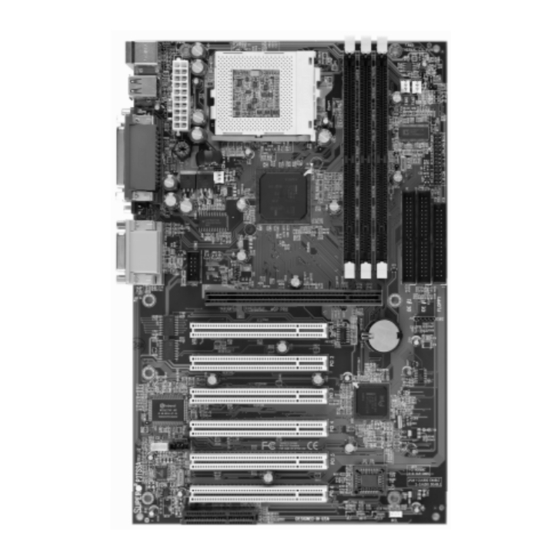
Page 9: Super P3Tssa Image
Chapter 1: Introduction SUPER P3TSSA Figure 1-1. SUPER P3TSSA Image... -
Page 10: Super P3Tssr Image
UPER P3TSSA/P3TSSR/P3TSSE User's Manual SUPER P3TSSR Figure 1-2. SUPER P3TSSR Image... -
Page 11: Super P3Tsse Image
Chapter 1: Introduction SUPER P3TSSE Figure 1-3. SUPER P3TSSE Image... -
Page 12: Super P3Tssa Layout
UPER P3TSSA/P3TSSR/P3TSSE User's Manual Figure 1-4. SUPER P3TSSA Layout MOUSE USB0/1 Parallel Port LINE LINE CD_1 AC'97 Audio CODEC chip CNR/USB3 (not drawn to scale) 7.8" PIII FCPGA or Celeron Processor GMCH AGP PRO PCI 1 PCI 2 PCI 3... - Page 13 P3TSSA Quick Reference Jumpers Description JBT1 CMOS Clear JP11/12 Front Side Bus Speed JP28 AC97 Audio JPWAKE Keyboard Wake-Up Connectors Description Audio CD Input (large connector) CD_1 Audio CD Input (small connector) Communications/Networking Riser COM1/COM2 COM1/COM2 Serial Port Connector CPU FAN...
-
Page 14: Super P3Tssr Layout
UPER P3TSSA/P3TSSR/P3TSSE User's Manual Figure 1-5. SUPER P3TSSR Layout JPWAKE CPU FAN KB/Mouse USB0/1 COM 1 PIII FCPGA or Celeron Processor LAN 1 LAN 2 JP35 JP31 JPA2 (not drawn to scale) ATX POWER GMCH BATTERY AGP 4x PCI 1... - Page 15 P3TSSR Quick Reference Jumpers Description JBT1 CMOS Clear JPA1 SCSI Channel A Termination JPA2 SCSI Channel B Termination JP11/12 Front Side Bus Speed JP31 LAN2 Enable/Disable JP34 SCSI Enable/Disable JP35 LAN1 Enable/Disable JP36 Speaker/Watchdog Enable JPWAKE Keyboard Wake-Up Connectors Description CH FAN 1 Chassis Fan Header COM1/COM2...
-
Page 16: Super P3Tsse Layout
UPER P3TSSA/P3TSSR/P3TSSE User's Manual Figure 1-6. SUPER P3TSSE Layout JPWAKE CPU FAN KB/Mouse USB0/1 COM 1 PIII FCPGA or Celeron Processor LAN 1 LAN 2 JP35 JP31 (not drawn to scale) ATX POWER GMCH BATTERY AGP 4x PCI 1 PCI 2... - Page 17 P3TSSE Quick Reference Jumpers Description JBT1 CMOS Clear JP11/12 Front Side Bus Speed JP31 LAN2 Enable/Disable JP35 LAN1 Enable/Disable JP36 Speaker/Watchdog Enable JPWAKE Keyboard Wake-Up Connectors Description CH FAN 1 Chassis Fan Header COM1/COM2 COM1/COM2 Serial Port Connector CPU FAN CPU Fan Header Infrared Device Header J1, J2, J3...
-
Page 18: Motherboard Features
UPER P3TSSA/P3TSSR/P3TSSE User's Manual Motherboard Features ® • Single Pentium III 500 MHz - 1.4 GHz processors at front bus speeds of 133/100 MHz, and single FCPGA and FCPGA2 Celeron processors at 100/66 MHz front side bus speeds Note: Please refer to the support section of our web site for a complete listing of supported processors. - Page 19 • BIOS flash upgrade utility • Drivers for 815/815E chipset utilities Dimensions • P3TSSA: ATX 12" x 7.8" (305 x 198 mm) • P3TSSR: ATX 12" x 8.7" (305 x 221 mm) • P3TSSE: ATX 12" x 7.8" (305 x 198 mm)
-
Page 20: E B-Step Chipset: System Block Diagram
UPER P3TSSA/P3TSSR/P3TSSE User's Manual 133/100/66 MHz Host Bus Graphics Performance Accelerator Audio Codec Modem Codec 1.5 Mb/sec SuperI/O Figure 1-7. 815E B-Step Chipset: NOTE: This is a general block diagram and may not exactly represent the features on your motherboard. See... -
Page 21: Chipset Overview
266 MB/sec. The MCH host interface bus runs at 133/100/66 MHz. I/O Controller Hub (ICH2) The P3TSSA/P3TSSR/P3TSSE is based on the 815E B-Step chipset and has the more powerful ICH2, which includes UDMA/100 IDE controllers and two USB controllers that offer 24 Mbps of bandwidth across four USB ports. -
Page 22: Special Features
The default setting is "Always OFF." Special Features Communication and Networking Riser (P3TSSA only) The CNR slot supports audio, modem and networking cards and provides interfaces that support multichannel audio, V.90 analog modems, home net- working through a telephone line, Ethernet 10/100 T-base networking and future communications technologies. - Page 23 The system BIOS is protected by hardware so that no virus can infect the BIOS area. The user can only change the BIOS content through the flash utility provided by SUPERMICRO. infecting the BIOS area and destroying valuable data. The overheat circuitry runs independently from...
-
Page 24: Acpi/Pc 98 Features
UPER P3TSSA/P3TSSR/P3TSSE User's Manual Auto-Switching Voltage Regulator for the CPU Core The auto-switching voltage regulator for the CPU core can support up to 20A of current and auto-sense voltage IDs ranging from 1.3v to 3.5v. This will allow the regulator to run cooler and thus make the system more stable. - Page 25 LAN traffic is kept to a minimum and users are not interrupted. The motherboards have a 3-pin header (WOL) to connect to the 3-pin header on a Network Interface Card (NIC) that has WOL capability.
-
Page 26: Power Supply
As with all computer products, a stable power source is necessary for proper and reliable operation. It is even more important for processors that have high CPU clock rates. The SUPER P3TSSA/P3TSSR/P3TSSE accommodates ATX power supplies. Although most power supplies generally meet the specifications required by the CPU, some are inadequate. - Page 27 Chapter 1: Introduction The Super I/O provides functions that comply with ACPI (Advanced Con- figuration and Power Interface), which includes support of legacy and ACPI power management through an SMI or SCI function pin. It also features auto power management to reduce power consumption. The IRQs, DMAs and I/O space resources of the Super I/O can flexibly adjust to meet ISA PnP requirements, which suppport ACPI and APM (Ad- vanced Power Management).
- Page 28 UPER P3TSSA/P3TSSR/P3TSSE User's Manual Notes 1-22...
-
Page 29: Chapter 2 Installation
Static-Sensitive Devices Electric-Static-Discharge (ESD) can damage electronic components. To pre- vent damage to your system board, it is important to handle it very carefully. The following measures are generally sufficient to protect your equipment from ESD. Precautions • Use a grounded wrist strap designed to prevent static discharge. •... -
Page 30: Processor Installation
UPER P3TSSA/P3TSSR/P3TSSE User’s Manual Processor Installation When handling the direct pressure on the label area of the fan. The following pages cover the installation procedure. You should install the processor in the motherboard first, then install the motherboard in the chas- sis, then the memory and add-on cards, and finally the cables and drivers. -
Page 31: Mounting The Motherboard In The Chassis
Figure 2-1. FCPGA Socket: Empty and with Processor Installed Mounting the Motherboard in the Chassis All motherboards have standard mounting holes to fit different types of chassis. Chassis may include a variety of mounting fasteners made of metal or plastic. Although a chassis may have both types, metal fasteners are the most highly recommended because they ground the motherboard to the chassis. -
Page 32: Installing Dimms
DIMM incorrectly. Gently press down on the DIMM module until it snaps into place. If installing only a single DIMM, you may use any Bank. The P3TSSA/ P3TSSR/P3TSSE will support a total of 512 MB of unbuffered SDRAM in its three DIMM slots. ECC type memory is not supported. PC133 and PC100 memory are both fully supported at their respective speeds. -
Page 33: Port/Control Panel Connector Locations
I/O ports. Mouse (Green) Keyboard COM1 Port (Purple) Ports (Turquoise) Figure 2-3a. I/O Port Locations: P3TSSA Mouse (Green) Keyboard USB Ports (Purple) Figure 2-3b. I/O Port Locations: P3TSSR/P3TSSE Top View of DIMM Slot Parallel Port (Burgundy) -
Page 34: Front Control Panel
UPER P3TSSA/P3TSSR/P3TSSE User’s Manual Front Control Panel JF1 and JF2 on the P3TSSA contain header pins for various front control panel connectors. The front control panel connections for the P3TSSE and P3TSSR are located on a single front control panel connector (JF1) and share the same layout. -
Page 35: Connecting Cables
To turn off the power when set to suspend mode, hold down the power button for at least 4 seconds. See Table 2-3 for pin definitions (P3TSSA). (see previous page for locations) ATX Power Supply Connector Pin Number Attach an... -
Page 36: Reset Connector
UPER P3TSSA/P3TSSR/P3TSSE User’s Manual Reset Connector The reset connectors are located on pins 12 & 13 of JF2. This con- nector attaches to the hardware reset switch on the computer case. See Table 2-4 for pin defini- tions (P3TSSA). Hard Drive LED The hard drive LED are located on pins 1-4 of JF1. -
Page 37: Speaker
(USB0 and USB1) are located on the motherboard backplane. Table 2-9 for pin definitions. addition, two additional USB head- ers (one on the P3TSSA) are pro- vided and designated USB2 and USB3. USBO and USB1 accept standard USB cables (not in- cluded). -
Page 38: Serial Ports
UPER P3TSSA/P3TSSR/P3TSSE User’s Manual Serial Ports Two connectors, for the COM1 and COM2 serial ports, are pro- vided on your board. COM1 is lo- cated beside the VGA port (see Figure 2-3) and COM2 is a header located near the backplane ports. -
Page 39: Chassis Intrusion Header
Fan Headers* The CPU, chassis and thermal control fan headers are desig- nated CPU FAN, FAN2 (Chassis FAN) and FAN3 (OH FAN). Refer to Table 2-13 for pin definitions. Chassis Intrusion The Chassis Intrusion header is lo- cated on JL1. See the board layouts in Chapter 1 for its location. -
Page 40: Jumper Settings
UPER P3TSSA/P3TSSR/P3TSSE User’s Manual Jumper Settings Explanation of Jumpers To modify the operation of the motherboard, jumpers can be used to choose between optional set- tings. Jumpers create shorts be- tween two pins to change the function of the connector. Pin 1 is identified with a square solder pad on the printed circuit board. -
Page 41: Cmos Clear
Replace JBT1 back to the pin 1-2 position be- fore powering up the system again. Do not use the PW_ON connector to clear CMOS. AC'97 (P3TSSA only) AC'97 brings high quality audio to PCs. When enabled with JP28, au- dio is processed onboard. -
Page 42: Keyboard Wake-Up
UPER P3TSSA/P3TSSR/P3TSSE User’s Manual Keyboard Wake-Up The JPWAKE jumper is used to- gether with the Keyboard Wake-Up function in BIOS. Enable both the jumper and the BIOS setting to al- low the system to be woken up by depressing a key on the keyboard. -
Page 43: Parallel Port, Agp, Floppy/Hard Disk Drive And Scsi Connections
Parallel Port Connector (P3TSSA only) The parallel (printer) port is lo- cated on J35. See Table 2-25 for pin definitions. -
Page 44: Floppy Connector
UPER P3TSSA/P3TSSR/P3TSSE User’s Manual Floppy Connector The floppy connector is located on JP26. See Table 2-26 for pin definitions. IDE Connectors There are no jumpers to config- ure the onboard IDE interfaces J18 and J19. Refer to Table 2- 27 for pin definitions. -
Page 45: Ultra160 Scsi Connectors
Ultra160 SCSI Connector (P3TSSR only) Refer to Table 2-28 for pin definitions for the Ultra160 SCSI connector located at JA1, JA2 and JA3. C onnector T a b le 2 -2 8 6 8 -p in U ltra 1 6 0 S C S I C o n n e c to rs (J A 1 , J A 2 , J A 3 ) C ontact N umber... -
Page 46: Agp Pro/4Xagp Slot
UPER P3TSSA/P3TSSR/P3TSSE User’s Manual AGP Pro/4xAGP Slot The AGP Pro slot is backward compatible with AGP and 4xAGP graphics cards, which have fewer pins than AGP Pro cards. Because of this, care must be taken when installing a graphics card into this slot, as doing so incorrectly can damage your motherboard. -
Page 47: Installing Software Drivers
Chapter 2: Installation Installing Software Drivers After all the hardware has been installed you must install the software drivers. The necessary drivers are all included on the Supermicro CD that came packaged with your motherboard. After inserting this CD into your CDROM drive, the display shown in Figure 2-5 should appear. -
Page 48: Chapter 3 Troubleshooting
Troubleshooting Procedures Use the following procedures to troubleshoot your system. followed all of the procedures below and still need assistance, refer to the ‘Technical Support Procedures’ and/or ‘Returning Merchandise for Service’ section(s) in this chapter. before adding, changing or installing any hardware components. Before Power On 1. -
Page 49: Memory Errors
Technical Support Procedures Before contacting Technical Support, please take the following steps. Also, note that as a motherboard manufacturer, Supermicro does not sell directly to end-users, so it is best to first check with your distributor or reseller for troubleshooting services. -
Page 50: Frequently Asked Questions
An example of a Technical Support form is on our web site: http://www.supermicro.com/techsupport/contact_support.htm 4. Distributors: For immediate assistance, please have your account number ready when placing a call to our technical support department. We can be reached by e-mail at support@supermicro.com or by fax at (408) 503-8019. Frequently Asked Questions Question:... - Page 51 UPER P3TSSA/P3TSSR/P3TSSE User’s Manual load the BIOS file to your computer. Unzip the BIOS update file and you will find the readme.txt (flash instructions), the fwhflash.com (BIOS flash utility) and the BIOS image (xxxxxx.rom) files. Copy these files onto a bootable floppy and reboot your system.
- Page 52 These devices are designed to work correctly while shar- ing IRQs. See Table 3-1 below for details on shared IRQs. P3TSSA PCI 1 shares an IRQ with PCI 5, the AGP Pro slot and onboard VGA PCI 2 shares an IRQ with PCI 6, onboard audio and SM bus*...
-
Page 53: Returning Merchandise For Service
UPER P3TSSA/P3TSSR/P3TSSE User’s Manual Question: I installed my microphone correctly but I can't record any sound. What should I do? Answer: Go to <Start>, <Programs>, <Accessories>, <Entertainment> and then <Volume Control>. devices in the menu and check the box beside "Microphone". -
Page 54: Chapter 4: Bios
Introduction This chapter describes the AMIBIOS for the P3TSSA/P3TSSR/P3TSSE. The AMIBIOS program is stored in a Flash EEPROM and can be easily upgraded using a floppy disk-based program. Note: Due to periodic changes to BIOS, some settings may have been added or deleted and might not yet be recorded in this manual. -
Page 55: Bios Features
UPER P3TSSA/P3TSSR/P3TSSE User’s Manual BIOS Features • Supports Plug and Play V1.0A and DMI 2.1 • Supports Intel PCI (Peripheral Component Interconnect) (PME) local bus specification • Supports Advanced Power Management (APM) specification v 1.1 • Supports ACPI • Supports Flash ROM AMIBIOS supports the LS120 drive made by Matsushita-Kotobuki Electronics Industries Ltd. - Page 56 The Main BIOS Setup Menu Press the <DEL> key during the POST (Power On Self Test) to enter the Main Menu of the BIOS Setup Utility. All Main Setup options are described in this section. The Main BIOS Setup screeen is displayed below. Main Advanced Chipset...
-
Page 57: Advanced Chipset Setup
UPER P3TSSA/P3TSSR/P3TSSE User’s Manual Advanced Chipset Setup Choose "Advanced BIOS Setup" from the "BIOS Setup Utility" main menu with the <Left> and <Right> arrow keys. You should see the following display. Select one of the items in the left frame of the screen, such as SuperIO Configuration, to go to the sub screen for that item. - Page 58 Chapter 4: BIOS CPU Overheat Warning This option allows you to "Enable" or "Disable" a system overheat warning signal, used to notify you in the event of a dangerous rise in heat levels. CPU Overheat Warning This option allows you to specify the temperature threshold that, when exceeded, will trigger the overheat warning alarm.
-
Page 59: Super Io Configuration
UPER P3TSSA/P3TSSR/P3TSSE User’s Manual Super IO Configuration After selecting the settings for "Health Monitor Features", use the <Up> and <Down> arrow keys to select the "SuperIO Configuration" line. When the "SuperIO Configuration" line is highlighted, press the <ENTER> key to display its menu. - Page 60 Chapter 4: BIOS Serial Port2 Mode This option specifies Serial Port2 Mode. The settings for this item include "Norma"l, "IRDA1.6ms", "IRDA311.6", "ASKIR", "ASKIR500", "ASKIRDem", "ASKIRD500." Parallel Port Address This option specifies the I/O address used by the parallel port. The settings for this item include "Disabled", "378', "278"...
-
Page 61: Ide Configuration
UPER P3TSSA/P3TSSR/P3TSSE User’s Manual Power Loss Control This option determines how the system will react when power is reapplied after being lost unexpectedly. The settings are "Always Off" if the sys- tem loses power unexpectedly, the computer system will keep power off until the power button is pressed), "Always On"... - Page 62 Chapter 4: BIOS Type This option sets the type of device that the AMIBIOS attempts to boot from after AMIBIOS POST is completed. The settings include "Not installed", "Auto", "CDROM" and "ARMD". "Auto" setting allows BIOS to automatically detect the pres ence of the IDE controller.
- Page 63 UPER P3TSSA/P3TSSR/P3TSSE User’s Manual "UWDMA2", "UWDMA3" and "UWDMA4." Select "Auto" to auto detect the DMA Mode. Select SWDMA0 through SWDMA2 to set single word DMA0 through DMA2. Select MWDMA0 through MWDMA2 to set Multi-word DMA0 through DMA2. Select "UDMA0" trhough "UDMA4" to set Ultra DMA0 through Ultra DMA4.
-
Page 64: Floppy Configuration
Chapter 4: BIOS Hard Disk Write Protect This item allows the user to prevent the hard disk from being overwritten. The options are "Enabled" and "Disabled." Enabled allows the drive to be used normally; read, write and erase functions can all be performed. Dis- abled prevents the hard disk from being erased. -
Page 65: Boot Settings Configuration
UPER P3TSSA/P3TSSR/P3TSSE User’s Manual Boot Settings Configuration Quick Boot This option allows the BIOS to skip certain tests that are normally perfomred on boot up. You can disable the option to speed up boot time. The settings are "Disabled" and "Enabled."... - Page 66 Chapter 4: BIOS System Keyboard This option is to let the system know if a keyboard is "Present' or "Ab- sent." Primary Display This option specifies the type of monitor display you have installed on the system. The settings are "Absent", "VGA/EGA", "Color 40 x 25", "Color 80 x 25"...
- Page 67 UPER P3TSSA/P3TSSR/P3TSSE User’s Manual Internal Cache This option is for enabling or disabling the internal CPU L1 cache. Settings include "Disabled", "Write-Thru" and "Write-Back." Disabled: This option prevents the system from using the internal CPU L1 cache. This setting should be used to slow the computer system down or to troubleshoot error messages.
-
Page 68: Event Log Configuration
Chapter 4: BIOS Event Log Configuration Event Logging This option Enables or Disables the logging of events. You can use this screen to select options for the Event Log Configuration Settings. You can access sub screens to view the event log and mark all events as read. Use the up and down arrow keys to select an item, and the plus <+>... -
Page 69: Chipset Setup
UPER P3TSSA/P3TSSR/P3TSSE User’s Manual Chipset Setup Choose "Chipset Setup" from the AMIBIOS "Setup Utility" main menu. The screen is shown below. All Chipset Setup options are described following the screen. You can use this screen to select options for the GHCH Configuration. - Page 70 Chapter 4: BIOS Internal Graphics Mode Select This option selects the mode for the internal graphics mode. Settings in- clude "Disabled", "Enabled; 512 KB" and "Enabled; 1 MB." Enabled; 1MB: This option allows the Internal Graphic controller to allocate 1 MB of system memory for video display use.
- Page 71 UPER P3TSSA/P3TSSR/P3TSSE User’s Manual Output Device Synch/Non-Synch This option allows you to set the output device as either "Non-Synchro- nous" (Asynchronous) or Synchronous. "Synchronous" means the output device will match the frequency of the bus speed. Asynchronous or Non- Synchronous allows data to be sent and received at a different frequency than the bus.
- Page 72 Chapter 4: BIOS RAS Timing This option regulates the speed of the Row Address Strobe (RAS) as either "Fast" or "Slow." As with CAS Latency, lowering the timing can increase the speed of the SDRAM, but at the expense of stability. RAS Pre-charge The precharge time is the number of cycles it takes for the RAS to accumu- late a charge before a DRAM refresh.
- Page 73 UPER P3TSSA/P3TSSR/P3TSSE User’s Manual DRAM Page Closing Policy The settings for this option are "Close" and "Open." Memory Hole Some ISA cards may require specific areas of memory to function. This can be done by choosing the 15 MB - 16 MB option to reserve the a r e a .
- Page 74 Chapter 4: BIOS CPU Bist Enable This option allows the CPU Bist Enable to be set. The settings are "Dis- abled" and "Enabled." ICH2 DCB Enable This option allows the ICH2 DCB to be set. The settings are "Disabled" and "Enabled." SMBus Controller The settings for this option are "Enabled"...
- Page 75 UPER P3TSSA/P3TSSR/P3TSSE User’s Manual Game Port This option allows the Game Port to be set. The settings are "Enabled" and "Disabled." LPC 4Eh-4Fh Decode This option allows the LPC 4Eh-4Fh to be set. The settings are "Disabled" and "Enabled." DMA-0 Type...
- Page 76 Chapter 4: BIOS CPU Latency Timer This option allows the CPU Latency Timer to be modified. he settings for this option are "Disabled" and "Enabled." Disabled: The deferrable proces- sor cycle will be deferred immediately after receiving another ADS#. abled: The deferrable processor cycle will only be deferred after it has been in a “Snoop Stall”...
-
Page 77: Pci Pnp Setup
UPER P3TSSA/P3TSSR/P3TSSE User’s Manual PCI PnP Setup Choose PCI/PnP Setup from the AMIBIOS Setup main menu. All PCI/PnP options are described in this section. The PCI/PnP Setup screen is shown below. Main Advanced Chipset Plug & Play O/S Reset Config Data... - Page 78 Chapter 4: BIOS PCI Latency Timer This option specifies the latency timing of the PCI clocks for all PCI devices. Settings include "32", "64", "96", "128", "160", "192", "224" and "248" PCI clocks. Allocate IRQ to PCI VGA This option lets you allocate an interrupt request (IRQ) to the PCI VGA adapter card (if used).
- Page 79 UPER P3TSSA/P3TSSR/P3TSSE User’s Manual Legacy USB Support This option allows Legacy USB support. The settings are "Disabled", "Enabled" and "Auto." Disabled prevents the use of any USB device in DOS or during system boot. Enabled allows the use of USB devices during boot and while using DOS.
- Page 80 Chapter 4: BIOS DMA Channel 0 DMA Channel 1 DMA Channel 3 DMA Channel 5 DMA Channel 6 DMA Channel 7 Each of the above list of DMA channel setting options can be set to "Avail- able" and "Reserved." Available means the specified DMA channel is avail- able for use by PCI/PnP devices.
-
Page 81: Power Setup
UPER P3TSSA/P3TSSR/P3TSSE User’s Manual Power Setup Choose "Power Setup" from the AMIBIOS "Setup Utility" main menu. Power Setup options are described in this section. The Power Setup screen is shown below. Main Advanced Chipset ACPI Aware O/S Suspend to RAM Support... - Page 82 Chapter 4: BIOS ACPI Aware O/S This option allows the system to utilize Intel's ACPI (Advanced Configuration and Power Interface) specification. Settings are "No" and "Yes." DOS®, Windows 3.x®, Windows 95 and Windows NT® are examples of non-ACPI aware operating systems. Windows 98®, Windows ME, and Windows 2000®...
- Page 83 UPER P3TSSA/P3TSSR/P3TSSE User’s Manual Suspend Power Saving Type The settings for this option are "C2" and "S1." The C2 setting allows the CPU (microprocessor) to be put in a low power state. In this state, incom- ing interrupts wake-up the CPU (microprocessor) to process them (I/O APIC).
- Page 84 Chapter 4: BIOS Green PC Monitor Power State This option specifies the power state that a green PC-compliant monitor enters when BIOS places it in a power saving state after the specified period of display inactivity has expired. The settings include "Standby", "Suspend"...
- Page 85 UPER P3TSSA/P3TSSR/P3TSSE User’s Manual THRM Throttle Ratio THRM throttling is used to lower power consumption and reduce heat. The settings include "87.5%", "75.0%", "62.5%", "50%", "37.5%", "25%" and "12.5%." Intruder Sel This option allows you to set the Intruder SEL setting to "SCI" or "SMI."...
- Page 86 Chapter 4: BIOS TCO Logic SMI Enable This allows the system to generate a System Management Interrupt when a century rollover occurs. The settings for this option "Disabled" and "En- abled." RTC Resume This allows you to direct the system to resume operation at a predetermined time by using the real-time clock.
-
Page 87: Boot Setup
UPER P3TSSA/P3TSSR/P3TSSE User’s Manual SMBUS Resume This allows you to wake up the system from a System Management Bus device. The settings for this option "Disabled" and "Enabled." LAN Wake-Up (370SSR/370SSE) This allows you to wake up LAN1 and LAN2 from a System Management Bus device. -
Page 88: Boot Device Priority
Boot Device Priority 1st Boot Device AMI BIOS automatically detects hardware devices of the system. This op- tion allows the BIOS to specify the order of boot sequence that is auto - detected by the BIOS. The settings for the 1st Boot Device are "Removeable Device", "Hard Drive", "ATAPI CDROM", "Onboard LAN1 Option", and "Onboard LAN2 Option."... -
Page 89: Security Setup
UPER P3TSSA/P3TSSR/P3TSSE User’s Manual Security Setup Choose "Security Setup" from the AMIBIOS "Setup Utility" main menu. All Security Setup options are described in this section. screen is shown below. Main Advanced Chipset Supervisor Password User Password > Change Supervisor Password >... -
Page 90: Boot Sector Virus Protection
Keep a record of the new password when the password is changed. If you forget the password, you must erase the system configuration informa- tion in the BIOS' CMOS. Change Supervisor Password This option allows you to change a supervisor password that was entered previously. -
Page 91: 4-10 Exit Setup
UPER P3TSSA/P3TSSR/P3TSSE User’s Manual 4-10 Exit Setup Choose "Exit Setup" from the AMIBIOS "Setup Utility" main menu. All Exit Setup options are described in this section. The Exit Setup screen is shown below. Main Advanced Chipset > Exit Saving Changes >... -
Page 92: Load Failsafe Defaults
Load Optimal Defaults Highlighting this setting and then pressing the <Enter> key provides the optimum performance settings for all devices and system features. Load Failsafe Defaults Highlighting this setting and then pressing the <Enter> key provides the safest set of parameters for the system. Use them if the system is behav- ing erratically. - Page 93 UPER P3TSSA/P3TSSR/P3TSSE User’s Manual Notes 4-40...
- Page 94 Appendix A: BIOS Error Beep Codes Appendix A BIOS Error Beep Codes & Messages During the POST (Power-On Self-Test) routines, which are performed each time the system is powered on, errors may occur. Non-fatal errors are those which, in most cases, allow the system to continue the boot-up process.
-
Page 95: Amibios Error Beep Codes
UPER P3TSSA/P3TSSR/P3TSSE User’s Manual AMI BIOS Error Beep Codes Beep Error Message Code 1 beep Refresh 2 beeps BIOS ROM file absent 3 beeps Base 64KB memory failure 4 beeps Flash program successful 5 beeps Media read error 6 beeps... -
Page 96: Amibios Post Codes
AMIBIOS POST Codes When AMIBIOS performs the Power On Self Test, it writes diagnostic codes checkpoint codes to I/O port 0080h. If the computer cannot complete the boot process, diagnostic equipment can be attached to the computer to read I/O port 0080h. Uncompressed Initialization Codes The uncompressed initialization checkpoint codes are listed in order of execution:... -
Page 97: Bootblock Recovery Codes
UPER P3TSSA/P3TSSR/P3TSSE User’s Manual Bootblock Recovery Codes The bootblock recovery checkpoint codes are listed in order of execution: Checkpoint Code Description The onboard floppy controller if available is initialized. Next, beginning the base 512 KB memory test. Initializing the interrupt vector table next. - Page 98 Uncompressed Initialization Codes The following runtime checkpoint codes are listed in order of execution. These codes are uncompressed in F0000h shadow RAM. Checkpoint Code Description The NMI is disabled. Next, checking for a soft reset or a power on condition. The BIOS stack has been built.
- Page 99 UPER P3TSSA/P3TSSR/P3TSSE User’s Manual Checkpoint Code Description Passing control to the video ROM to perform any required configuration before the video ROM test. All necessary processing before passing control to the video ROM is done. Looking for the video ROM next and passing control to it.
- Page 100 Checkpoint Code Description Preparing the descriptor tables next. The descriptor tables are prepared. Entering protected mode for the memory test next. Entered protected mode. Enabling interrupts for diagnostics mode next. Interrupts enabled if the diagnostics switch is on. Initializing data to check memory wraparound at 0:0 next.
- Page 101 UPER P3TSSA/P3TSSR/P3TSSE User’s Manual Checkpoint Code Description The A20 address line, parity, and the NMI are disabled. Adjusting the memory size depending on relocation and shadowing next. The memory size was adjusted for relocation and shadowing. Clearing the Hit <DEL> message next.
- Page 102 Checkpoint Code Description The programming after WINBIOS Setup has completed. Displaying the power on screen message next. The first screen message has been displayed. The <WAIT...> message is displayed. Performing the PS/2 mouse check and extended BIOS data area allocation check next. Programming the WINBIOS Setup options next.
- Page 103 UPER P3TSSA/P3TSSR/P3TSSE User’s Manual Checkpoint Code Description Returned after setting the RS-232 base address. Performing any required initialization before the Coprocessor test next. Required initialization before the Coprocessor test is over. Initializing the Coprocessor next. Coprocessor initialized. Performing any required initialization after the Coprocessor test next.
-
Page 104: Bus Checkpoint Codes
Bus Checkpoint Codes The system BIOS passes control to different buses at the following checkpoints: Checkpoint Code Description Initializing the different bus system, static, and output devices, if present. Initialized bus input, IPL, and general devices, if present. Displaying bus initialization error messages, if any. Initializing bus adaptor ROMs from C8000h through D8000h. - Page 105 UPER P3TSSA/P3TSSR/P3TSSE User’s Manual Notes B-10...
Need help?
Do you have a question about the SUPER P3TSSA and is the answer not in the manual?
Questions and answers