Table of Contents
Advertisement
Quick Links
Advertisement
Table of Contents

Related Manuals for National Instruments NI 5734


Summary of Contents for National Instruments NI 5734
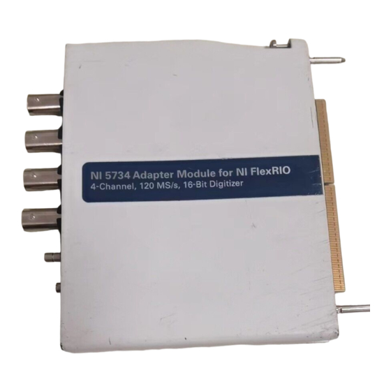
- Page 1 NI-5734...
-
Page 2: Table Of Contents
NI 5732—2 analog input, 14-bit, 80 MS/s digitizer • • NI 5733—2 analog input, 16-bit, 120 MS/s digitizer NI 5734—4 analog input, 16-bit, 120 MS/s digitizer • Contents Electromagnetic Compatibility Guidelines..................2 How to Use Your NI FlexRIO Documentation Set ................3 Front Panel and Connector Pinouts ..................... -
Page 3: Electromagnetic Compatibility Guidelines
Caution To ensure the specified EMC performance, install the included snap-on ferrite bead (National Instruments part number 711856-01) on any cable attached to the AUX I/O connector in accordance with the instructions listed in the Appendix: Installing EMI Controls section. -
Page 4: How To Use Your Ni Flexrio Documentation Set
Other Useful Information on ni.com ni.com/ipnet Contains LabVIEW FPGA functions and intellectual property to share. ni.com/flexrio Contains product information and data sheets for NI FlexRIO devices. These documents are also available at ni.com/manuals © National Instruments Corporation NI 5731/5732/5733/5734R User Guide and Specifications... -
Page 5: Front Panel And Connector Pinouts
50 single-ended analog input channel 0. AI 0 50 single-ended analog input channel 1. AI 1 50 single-ended analog input channel 2 (NI 5734 only). AI 2 50 single-ended analog input channel 3 (NI 5734 only). AI 3 Reference or external clock input, 50 ... - Page 6 HDMI interface. Do not connect the AUX I/O port on the NI 5731/5732/5733/5734 into the HDMI port of another device. NI is not liable for any damage resulting from such signal connections. © National Instruments Corporation NI 5731/5732/5733/5734R User Guide and Specifications...
-
Page 7: Block Diagram
Block Diagram Figure 3 shows the NI 5731/5732/5733/5734 block diagram and signal flow to and from the NI 5731/5732/5733/5734 component-level intellectual property (CLIP) by way of the adapter module and the corresponding CLIP in LabVIEW FPGA. NI 5731/5732/5733/5734 Adapter Module LabVIEW FPGA CLIP DC Over Voltage ADC Data... -
Page 8: Ni 5731/5732/5733/5734 Component-Level Intellectual Property (Clip)
Adapter Socketed CLIP FPGA VI Fixed I/O Module CLIP DRAM 0 DRAM 1 CLIP Socket CLIP Socket Socketed Socketed CLIP CLIP DRAM0 DRAM1 Figure 4. CLIP and FPGA VI Relationship © National Instruments Corporation NI 5731/5732/5733/5734R User Guide and Specifications... -
Page 9: Cables
The NI 5731/5732/5733/5734 CLIP items provides access to two analog input channels (four analog input channels on the NI 5734), eight bidirectional DIO channels, four bidirectional PFI channels, and an input clock selector that can be configured to use one of the following settings: •... -
Page 10: Clocking
NI 5733 Min = 50 MHz NI 5733 Max = 120 MHz NI 5734 Min = 50 MHz NI 5734 Max = 120 MHz Duty Cycle Stabilizer (DCS) enabled. DCS enabled is the default setting for all NI 5731/5732/5733/5734 CLIP items. You can disable the DCS by adjusting register 9 in the ADC. -
Page 11: Using Your Device With A Labview Fpga Example Vi
Using Your Device with a LabVIEW FPGA Example VI Note You must install the NI FlexRIO Adapter Module Support software before running this example. Refer to the NI FlexRIO FPGA Module Installation Guide and Specifications for more information about installing your software. The NI FlexRIO Adapter Module Support software includes a variety of example projects to help get you started creating your LabVIEW FPGA application. - Page 12 , and select the article, Ignoring a Particular Error in an Error Cluster in LabVIEW. 3BPD5HRY To reinitialize the FPGA, refer to the Reset (Invoke Method) topic in the NI FPGA Module Help file, available in LabVIEW and at ni.com/manuals © National Instruments Corporation NI 5731/5732/5733/5734R User Guide and Specifications...
-
Page 13: Creating A Labview Project And Running A Vi On An Fpga Target
Creating a LabVIEW Project and Running a VI on an FPGA Target This section explains how to set up your target and create an FPGA VI and host VI for data communication. For more detailed information about acquiring data on your NI 5731/5732/5733/5734, refer to the device specific examples available in NI Example Finder. - Page 14 12. Wire the error out terminal of the Open FPGA VI Reference function to the error in control of the Read/Write Control function. 13. Configure the Read/Write Control function by clicking the terminal section labeled Unselected, and selecting IO Module/AI 0 Data N. © National Instruments Corporation NI 5731/5732/5733/5734R User Guide and Specifications...
- Page 15 14. Wire an indicator to the output terminal of the IO Module\AI 0 Data N node. 15. Add the Close FPGA VI Reference function, located on the FPGA Interface palette, to the right of the While Loop on the block diagram. 16.
-
Page 16: Specifications
Analog Input (AI 0, AI 1, AI 2, and AI 3) General Characteristics Number of channels ..........Two (four channels on the NI 5734) Connector type ............BNC Input type ...............Simultaneously sampled, singled-ended Input impedance.............50 , per connector Input coupling (software selectable)......AC or DC... - Page 17 Typical Specifications ADC DC offset NI 5731 ............±5.2 mV NI 5732 ............±6.6 mV NI 5733/5734 ..........±7.1 mV DC-coupled common-mode output .......±0.8 mV (50 terminated) Full Scale Input Table 5. Full Scale Input Gain = 6 dB Gain = 12 dB Device Gain = 0 dB (FS at 0 dB divided by 2)
- Page 18 –87.1 dBc –87.1 dBc –84.1 dBc NI 5732 9.7 MHz –83.9 dBc –87.7 dBc –89.5 dBc NI 5733/5734 9.7 MHz –80.5 dBc –85.0 dBc –86.0 dBc Measured at –1 dBFS. © National Instruments Corporation NI 5731/5732/5733/5734R User Guide and Specifications...
- Page 19 For NI 5731/5732 devices only, the crosstalk is 4 dB worse than the values in Table 13 when you configure both channels to use filters. Table 14. NI 5734 only: AI Channel Crosstalk Receiver Channel (50 terminated) Channel Path (N ± 2) Channel Path (N ±...
- Page 20 Phase adjust DAC range NI 5731 ............406 ± 13 degrees NI 5732 ............427 ± 13 degrees NI 5733/5734 ..........429 ± 9 degrees Frequency adjust DAC range .........±160 ppm Data rate (IOModuleClock0) .........Sample rate © National Instruments Corporation NI 5731/5732/5733/5734R User Guide and Specifications...
- Page 21 Measurements Frequency Response –1 –2 –3 –4 –5 –6 10 k 100 k Frequency ( Hz ) Figure 8. AC-Coupled Low Frequency Response (Multiple Channels Overlaid) –1 –2 –3 –4 –5 –6 –7 NI 5731 NI 5732 NI 5733/5734 –8 Frequency ( MHz ) Figure 9.
- Page 22 Figure 10. Elliptic Filter Frequency Response (Multiple Channels Overlaid) –1 –2 –3 –4 –5 NI 5731 NI 5732 NI 5733/5734 –6 Frequency ( MHz ) Figure 11. Elliptic Filter Frequency Response: 0 to –6 dB (Multiple Channels Overlaid) © National Instruments Corporation NI 5731/5732/5733/5734R User Guide and Specifications...
- Page 23 –10 –20 –30 –40 –50 –60 –70 –80 NI 5731 NI 5732 NI 5733/5734 –90 Frequency ( MHz ) Figure 12. Bessel Filter Frequency Response (Multiple Channels Overlaid) –1 –2 –3 –4 –5 NI 5731 NI 5732 NI 5733/5734 –6 Frequency ( MHz ) Figure 13.
- Page 24 Figure 14. NI 5731 Elliptic Filter Group Delay (12 Channels Overlaid) –1 –2 –3 –4 –5 Frequency ( MHz ) Figure 15. NI 5731 Bessel Filter Group Delay (12 Channels Overlaid) © National Instruments Corporation NI 5731/5732/5733/5734R User Guide and Specifications...
- Page 25 NI 5732 Group Delay –1 Frequency ( MHz ) Figure 16. NI 5732 Elliptic Filter Group Delay (12 Channels Overlaid) –1 –2 –3 –4 –5 Frequency ( MHz ) Figure 17. NI 5732 Bessel Filter Group Delay (12 Channels Overlaid) NI 5731/5732/5733/5734R User Guide and Specifications ni.com...
- Page 26 Figure 18. NI 5733/5734 Elliptic Filter Group Delay (44 Channels Overlaid) –1 –2 –3 –4 –5 –6 Frequency ( MHz ) Figure 19. NI 5733/5734 Bessel Filter Group Delay (44 Channels Overlaid) © National Instruments Corporation NI 5731/5732/5733/5734R User Guide and Specifications...
- Page 27 Analog Input Total Phase Noise NI 5731 –100 –110 –120 –130 –140 –150 100k Frequency Offset (Hz) from 10 MHz Carrier Figure 20. NI 5731 AI Phase Noise (10 MHz Input, PLL Unlocked, Onboard Oscillator, 618 FS RMS Jitter) NI 5732 –100 –110 –120...
- Page 28 Frequency Offset (Hz) from 40 MHz Carrier Figure 23. NI 5733/5734 AI Phase Noise (40 MHz Input, PLL Locked to PXI 10 MHz Reference Clock, Onboard Oscillator, 448 FS RMS Jitter) © National Instruments Corporation NI 5731/5732/5733/5734R User Guide and Specifications...
- Page 29 Terminated Spectral Measurements (16,382 point FFT, 30 Average RMS) NI 5731 –10 –20 –30 –40 –50 –60 –70 –80 –90 –100 –110 –120 Frequency (MHz) Figure 24. NI 5731 Gain at 0 dB; Elliptic, Bessel, or Filter Bypass; AC- or DC-coupled –10 –20 –30...
- Page 30 –10 –20 –30 –40 –50 –60 –70 –80 –90 –100 –110 –120 Frequency (MHz) Figure 27. NI 5732 Gain at 12 dB; Elliptic, Bessel, or Filter Bypass; AC- or DC-coupled © National Instruments Corporation NI 5731/5732/5733/5734R User Guide and Specifications...
- Page 31 NI 5733/5734 –10 –20 –30 –40 –50 –60 –70 –80 –90 –100 –110 –120 Frequency (MHz) Figure 28. NI 5733/5734 Gain at 0 dB; Elliptic, Bessel, or Filter Bypass; AC- or DC-coupled –10 –20 –30 –40 –50 –60 –70 –80 –90 –100 –110...
- Page 32 –50 –60 –70 –80 –90 –100 –110 Frequency (MHz) Figure 31. NI 5731 Gain at 12 dB: –1 dBFS at 4.9 MHz, –93 dBc SFDR, Bypass Filter, 100 Averages RMS © National Instruments Corporation NI 5731/5732/5733/5734R User Guide and Specifications...
- Page 33 –10 –20 –30 –40 –50 –60 –70 –80 –90 –100 –110 Frequency (MHz) Figure 32. NI 5731 Gain at 12 dB: –1 dBFS at 4.9 MHz, –93 dBc SFDR, Bypass Filter, 10 Averages RMS NI 5732 –10 –20 –30 –40 –50 –60 –70...
- Page 34 –50 –60 –70 –80 –90 –100 –110 Frequency (MHz) Figure 35. NI 5732 Gain at 12 dB: –1 dBFS at 9.7 MHz, –94 dBc SFDR, Bypass Filter, 10 Averages RMS © National Instruments Corporation NI 5731/5732/5733/5734R User Guide and Specifications...
- Page 35 NI 5733/5734 –10 –20 –30 –40 –50 –60 –70 –80 –90 –100 –110 Frequency (MHz) Figure 36. NI 5733/5734 Gain at 0 dB: –1 dBFS at 20.1 MHz, –85 dBc SFDR, Bypass Filter, 100 Averages RMS –10 –20 –30 –40 –50 –60 –70...
- Page 36 –100 –110 Frequency (MHz) Figure 39. NI 5732 at 12 dB Gain and Filter Bypass: –83 dBc, f = 19.6 MHz (–7 dBFS), 20.8 MHz (–7 dBFS), 100 Average RMS © National Instruments Corporation NI 5731/5732/5733/5734R User Guide and Specifications...
- Page 37 –10 –20 –30 –40 –50 –60 –70 –80 –90 –100 –110 Frequency (MHz) Figure 40. NI 5733/5734 at 12 dB Gain and Filter Bypass: –81 dBc, f = 19.6 MHz (–7 dBFS), 20.8 MHz Internal Sample Clock General Characteristics Clock distribution part number ......AD9511 ;...
- Page 38 NI 5733 Min = 50 MHz NI 5733 Max = 120 MHz NI 5734 Min = 50 MHz NI 5734 Max = 120 MHz Duty Cycle Stabilizer (DCS) enabled. DCS enabled is the default setting for all NI 5731/5732/5733/5734 CLIP items. You can disable the DCS by adjusting register 9 in the ADC.
- Page 39 Physical Dimensions ............12.9 2.0 12.1 cm (5.1 0.8 4.7 in.) Weight NI 5731/5732/5733 ........313 g (11.0 oz) NI 5734 ............332 g (11.7 oz) Front panel connectors...........BNC, SMB, and HDMI NI 5731/5732/5733/5734R User Guide and Specifications ni.com...
- Page 40 For PXI/PXI Express chassis configurations that group NI FlexRIO adapter modules in three or more contiguous slots, National Instruments recommends limiting the ambient operating temperature to less than 50 C. © National Instruments Corporation NI 5731/5732/5733/5734R User Guide and Specifications...
- Page 41 Electromagnetic Compatibility This product meets the requirements of the following EMC standards for electrical equipment for measurement, control, and laboratory use: • EN 61326-1 (IEC 61326-1): Class A emissions; Basic immunity • EN 55011 (CISPR 11): Group 1, Class A emissions •...
-
Page 42: Where To Go For Support
National Instruments corporate headquarters is located at 11500 North Mopac Expressway, Austin, Texas, 78759-3504. National Instruments also has offices located around the world to help address your support needs. For telephone support in the United States, create your service request at ni.com/ support and follow the calling instructions or dial 512 795 8248. -
Page 43: Appendix: Installing Emi Controls
For more installation information, refer to the NI FlexRIO FPGA Module Installation Guide and Specifications. Installing PXI EMC Filler Panels Complete the following instructions to install PXI EMC filler panels (National Instruments part number 778700-01) in your PXI chassis: Remove the captive screw covers. - Page 44 For patents covering National Instruments products/technology, refer to the appropriate location: Help»Patents in your software, the patents.txt file on your media, or the National Instruments Patent Notice at ni.com/patents. Refer to the Export Compliance Information at ni.com/legal/ export-compliance for the National Instruments global trade compliance policy.
Need help?
Do you have a question about the NI 5734 and is the answer not in the manual?
Questions and answers