Table of Contents
Advertisement
Quick Links
A V T E C H
E L E C T R O S Y S T E M S
L T D .
N A N O S E C O N D
W A V E F O R M
E L E C T R O N I C S
S I N C E
1 9 7 5
info@avtechpulse.com
Tel: 888-670-8729 (USA & Canada)
BOX 5120, LCD MERIVALE
http://www.avtechpulse.com/
or +1-613-686-6675 (Worldwide)
OTTAWA, CANADA K2C3H5
INSTRUCTIONS
MODEL AVRQ-5-B
KILOVOLT PULSE GENERATOR
WITH dV/dt RATES
EXCEEDING 100 kV/us
FOR COMMON MODE TRANSIENT IMMUNITY (CMTI) TESTS
SERIAL NUMBER:
14320
Advertisement
Table of Contents

Related Manuals for AVTECH ELECTROSYSTEMS AVRQ-5-B


Summary of Contents for AVTECH ELECTROSYSTEMS AVRQ-5-B
- Page 1 1 9 7 5 info@avtechpulse.com Tel: 888-670-8729 (USA & Canada) BOX 5120, LCD MERIVALE http://www.avtechpulse.com/ or +1-613-686-6675 (Worldwide) OTTAWA, CANADA K2C3H5 INSTRUCTIONS MODEL AVRQ-5-B KILOVOLT PULSE GENERATOR WITH dV/dt RATES EXCEEDING 100 kV/us FOR COMMON MODE TRANSIENT IMMUNITY (CMTI) TESTS SERIAL NUMBER: 14320...
-
Page 2: Warranty
WARRANTY Avtech Electrosystems Ltd. warrants products of its manufacture to be free from defects in material and workmanship under conditions of normal use. If, within one year after delivery to the original owner, and after prepaid return by the original owner, this Avtech product is found to be defective, Avtech shall at its option repair or replace said defective item. -
Page 3: Table Of Contents
TABLE OF CONTENTS WARRANTY........................2 TECHNICAL SUPPORT....................2 TABLE OF CONTENTS....................3 INTRODUCTION......................6 HIGH-VOLTAGE PRECAUTIONS..................8 SPECIFICATIONS......................9 REGULATORY NOTES....................10 FCC PART 18........................10 EC DECLARATION OF CONFORMITY................10 DIRECTIVE 2011/65/EU (RoHS)...................11 DIRECTIVE 2002/96/EC (WEEE)..................11 FIRMWARE LICENSING.......................12 INSTALLATION......................13 VISUAL CHECK........................13 POWER RATINGS........................ 13 CONNECTION TO THE POWER SUPPLY................13 PROTECTION FROM ELECTRIC SHOCK................14 ENVIRONMENTAL CONDITIONS..................15... - Page 4 DUT INSTALLATION....................33 SOCKET PINOUT......................... 33 DAUGHTERBOARD PINOUT....................34 DAUGHTERBOARD COMPONENTS...................36 SO-8 DAUGHTERBOARD (PCB 314B)................38 CUSTOMER-SPECIFIC PCB 324B DAUGHTERBOARD.............39 CUSTOM DAUGHTERBOARDS...................40 DIFFERENTIAL PROBING....................40 INSTALLING THE DAUGHTERBOARDS................41 BASIC TEST ARRANGEMENTS..................42 INTER-CHANNEL INTERFERENCE..................44 TYPICAL WAVEFORMS FOR STANDARD DAUGHTERBOARDS......45 BASIC THEORY........................45 CONTROLLING THE TRANSITION TIME................46 TYPICAL POSITIVE RESULTS, WITH NO DUT INSTALLED..........47 TYPICAL NEGATIVE RESULTS, WITH NO DUT INSTALLED..........48 TYPICAL POSITIVE RESULTS (-XHV UNITS)..............49...
- Page 5 DUT WIRING, ON STANDARD DAUGHTERBOARD (PCB 267D)........77 DUT WIRING, ON SO8 DAUGHTERBOARD (PCB 314B)...........78 DUT WIRING, ON CUSTOMER-SPECIFIC DAUGHTERBOARD (PCB 324B)....79 MAIN WIRING........................80 PERFORMANCE CHECK SHEET................81 Manual Reference: /fileserver1/officefiles/instructword/avrq-5/AVRQ-5-B,ed21.odt. Last modified March 1, 2023. Copyright © 2023 Avtech Electrosystems Ltd, All Rights Reserved.
-
Page 6: Introduction
INTRODUCTION The AVRQ-5-B is designed to test the common mode transient immunity (CMTI) of optocouplers. The standard AVRQ-5-B can generate -1.5 or +1.5 kV pulses. The unloaded switching time (10%-90%) is fixed at ≤ 10 ns. The transition time may be increased to at least 50 ns by adding high-voltage capacitors across the device under test (by soldering it to the DUT daughterboard). - Page 7 Coaxial cabling should not be used, because it will introduce too much parasitic capacitance. The AVRQ-5-B features front panel keyboard and adjust knob control of the output pulse parameters along with a four line by 40-character backlit LCD display of the rise time, pulse width, pulse delay, and pulse repetition frequency.
-
Page 8: High-Voltage Precautions
HIGH-VOLTAGE PRECAUTIONS CAUTION: This instrument provides output voltages as high as 1500 or 2000 Volts under normal operating conditions, so extreme caution must be employed when using this instrument. The instrument should only be used by individuals who are thoroughly skilled in high voltage laboratory techniques. -
Page 9: Specifications
SPECIFICATIONS Model: AVRQ-5-B High-Voltage Pulse Amplitude: Standard: -1.5 or +1.5 kV (HV pulse / GND1) with -AHV option: -1 kV to -1.5 kV, +1 kV to +1.5 kV, in ≤ 1V steps with -XHV option: -1.5 kV to -2 kV, -1.5 kV to -2 kV, in ≤ 1V steps Load resistance: >... -
Page 10: Regulatory Notes
This instrument does not normally require regular maintenance to minimize interference potential. However, if loose hardware or connectors are noted, they should be tightened. Contact Avtech (info@avtechpulse.com) if you require assistance. EC DECLARATION OF CONFORMITY Avtech Electrosystems Ltd. P.O. Box 5120, LCD Merivale Ottawa, Ontario Canada K2C 3H5 declare that this pulse generator meets the intent of Directive 2004/108/EG for Electromagnetic Compatibility. -
Page 11: Directive 2011/65/Eu (Rohs)
(also known as “RoHS Recast”). In addition, this declaration of conformity is issued under the sole responsibility of Avtech Electrosystems Ltd. Specifically, products manufactured do not contain the substances listed in the table below in concentrations greater than the listed maximum value. -
Page 12: Firmware Licensing
laws) on behalf of the customer, as provided for under Article 9 of Directive 2002/96/EC. Customers who have purchased Avtech equipment through local representatives should consult with the representative to determine who has responsibility for WEEE compliance. Normally, such responsibilities with lie with the representative, unless other arrangements (under Article 9) have been made. -
Page 13: Installation
INSTALLATION VISUAL CHECK After unpacking the instrument, examine to ensure that it has not been damaged in shipment. Visually inspect all connectors, knobs, liquid crystal displays (LCDs), and the handles. Confirm that a power cord, a GPIB cable, and two instrumentation manuals (this manual and the “Programming Manual for -B Instruments”) are with the instrument. -
Page 14: Protection From Electric Shock
Destination Region Description Option Manufacturer Part Number United Kingdom, Hong Kong, BS 1363, -AC00 Qualtek 370001-E01 Singapore, Malaysia 230V, 50 Hz AS 3112:2000, Australia, New Zealand -AC01 Qualtek 374003-A01 230-240V, 50 Hz Continental Europe, Korea, European CEE 7/7 -AC02 Qualtek 364002-D01 Indonesia, Russia “Schuko”... -
Page 15: Environmental Conditions
ENVIRONMENTAL CONDITIONS This instrument is intended for use under the following conditions: 1. indoor use; 2. altitude up to 2 000 m; 3. temperature 5 °C to 40 °C; 4. maximum relative humidity 80 % for temperatures up to 31 °C decreasing linearly to 50 % relative humidity at 40 °C;... -
Page 16: Fuses
FUSES This instrument contains four fuses. All are accessible from the rear-panel. Two protect the AC prime power input, and two protect the internal DC power supplies. The locations of the fuses on the rear panel are shown in the figure below: Fuses #1 and #2 Fuse #4 Fuse #3... -
Page 17: Dc Fuse Replacement
DC FUSE REPLACEMENT The DC fuses may be replaced by inserting the tip of a flat-head screwdriver into the fuse holder slot, and rotating the slot counter-clockwise. The fuse and its carrier will then pop out. FUSE RATINGS The following table lists the required fuses: Recommended Replacement Part Nominal Fuses... -
Page 18: Chassis Configurations
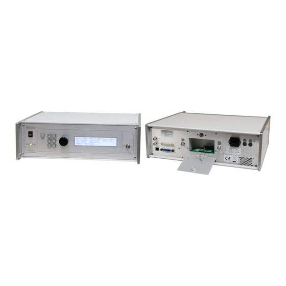
CHASSIS CONFIGURATIONS The AVRQ-5-B is offered with two basic chassis configurations. The standard model is provided in a “3U” height (in rack units) enclosure, with the DUT area located on the rear panel. The DUT area may optionally be moved to the front panel by specifying the -FPD option. -
Page 19: Front Panel Controls (Units Without -Fpd Option)
FRONT PANEL CONTROLS (UNITS WITHOUT -FPD OPTION) 1. POWER Switch . This is the main power switch. When turning the instrument on, there is normally a delay of 10 seconds before anything is shown on the main display, as the internal operating system boots up. 2. - Page 20 5. KEYPAD . Control Name Function MOVE This moves the arrow pointer on the display. CHANGE This is used to enter the submenu, or to select the operating mode, pointed to by the arrow pointer. ×10 If one of the adjustable numeric parameters is displayed, this increases the setting by a factor of ten.
-
Page 21: Rear Panel Controls (Units Without -Fpd Option)
REAR PANEL CONTROLS (UNITS WITHOUT -FPD OPTION) GATE VCC2 PULSE LOGIC TRIG RS-232 GPIB Note: some connectors may be in different positions than shown above, depending on the exact combination of options ordered. 1. AC POWER INPUT . An IEC-320 C14 three-pronged recessed male socket is provided on the back panel for AC power connection to the instrument. - Page 22 triggers on the rising edge of this input. The input impedance of this input is 1 kΩ. (Depending on the length of cable attached to this input, and the source driving it, it may be desirable to add a coaxial 50 Ohm terminator to this input to provide a proper transmission line termination.
- Page 23 high-voltage probe with the 013-0291-00 probe-tip-to-BNC adapter, or a similar arrangement. DO NOT CONNECT COAXIAL CABLING TO THIS OUTPUT. The capacitance of the cabling will reduce the dV/dt rates noticeably. 11. LOGIC OUT Connectors . There are three possible positions where the logic probe can be connected, “A”, “B”, and “C”.
-
Page 24: Front Panel Controls (Units With -Fpd Option)
FRONT PANEL CONTROLS (UNITS WITH -FPD OPTION) 1. POWER Switch . This is the main power switch. When turning the instrument on, there is normally a delay of 10 seconds before anything is shown on the main display, as the internal operating system boots up. 2. - Page 25 3. SYNC OUT . This connector supplies a SYNC output that can be used to trigger other equipment, particularly oscilloscopes. This signal leads (or lags) the main output by a duration set by the "DELAY" controls and has an approximate amplitude of +3 Volts to R >...
- Page 26 CAUTION: Voltages as high as 2 kV may be present on the center conductor of this output connector. Avoid touching this conductor. Connect to this connector using a Tektronix P5100 high-voltage probe with the 013-0291-00 probe-tip-to-BNC adapter, or a similar arrangement, to ensure that the center conductor is not exposed.
- Page 27 measure the signals separately, and use the memory storage function of the oscilloscope if you wish to combine the signals on a single image. 9. VCC2 OUT Connector . (Optional feature. Present on units with the -V2 option only.) This output is wired in parallel with the VCC2 connection on the DUT socket, and may be used for monitoring purposes.
-
Page 28: Rear Panel Controls (Units With -Fpd Option)
REAR PANEL CONTROLS (UNITS WITH -FPD OPTION) GATE TRIG RS-232 GPIB Note: some connectors may be in different positions than shown above, depending on the exact combination of options ordered. 1. AC POWER INPUT . An IEC-320 C14 three-pronged recessed male socket is provided on the back panel for AC power connection to the instrument. - Page 29 edge of this input. The input impedance of this input is 1 kΩ. (Depending on the length of cable attached to this input, and the source driving it, it may be desirable to add a coaxial 50 Ohm terminator to this input to provide a proper transmission line termination.
-
Page 30: General Information
GENERAL INFORMATION BASIC PULSE CONTROL This instrument can be triggered by its own internal clock or by an external TTL trigger signal. In either case, two output channels respond to the trigger: HV PULSE and SYNC. The HV PULSE channel is the signal that is applied to the DUT. The SYNC pulse is a fixed-width TTL-level reference pulse used to trigger oscilloscopes or other measurement systems. -
Page 31: Trigger Modes
The next figure illustrates the relationship between the signals when an external TTL- level trigger is used: > 50 ns TRIG TTL LEVELS (external input) (0V and 3V-5V) PROPAGATION DELAY (FIXED) 100 ns, FIXED SYNC OUT 3V, FIXED PULSE FALL TIME DELAY >... -
Page 32: Gating Modes
These modes can be selected using the front panel trigger menu, or by using the appropriate programming commands. (See the “Programming Manual for -B Instruments” for more details.) GATING MODES Triggering can be suppressed by a TTL-level signal on the rear-panel GATE connector. The instrument can be set to stop triggering when this input high or low, using the front- panel gate menu or the appropriate programming commands. -
Page 33: Dut Installation
An arrangement of pin sockets on the main motherboard accepts these daughterboards. The AVRQ-5-B mainframe provides the high-voltage common mode pulse (which is tied to GND1), and VCC2 / GND2 (the non-floating output-side power supply). The user is responsible for configuring the daughterboards to implement the correct input side power (VCC1), biasing, filtering, loading, socketing, and glitch measurement. -
Page 34: Daughterboard Pinout
The socket and the sample daughterboards are designed so that the daughterboard can be installed in two positions – one for positive pulse mode, and one for negative pulse mode. Two physical positions are used to achieve polarity switching, rather than using internal high-voltage relays, in order to achieve the fastest possible switching times. - Page 35 For positive pulse mode, the “AMP1” front-panel setting must be set to a positive value AND the daughterboard must be installed in the socket so that it is in the left-most position (when viewed from the DUT area door opening), like this: The left-most four GND2 pin sockets are used in the positive orientation.
-
Page 36: Daughterboard Components
The right-most four GND2 pin sockets are used in the negative orientation. NEGATIVE DAUGHTERBOARD INSTALLED FOR PULSE OPERATION THESE ARE THE ONLY TWO CORRECT POSITIONS. THE BOARDS WILL NOT MATE IN ANY OTHER CONFIGURATION. Two circuit diagrams in the BASIC TEST ARRANGEMENTS section (page 42) show how the socket and daughterboard pins mesh in the two polarity configurations, electrically. - Page 37 Resistor footprints R4 and R6 allow either pin 6 or 7 (or both) of the DUT to be used as the logic output. R2 can be used to pull-up the DUT output (if it is an open-collector output, in particular) and C6 can be used to add a load capacitance to the logic output. These component values are sometimes specified by particular test standards.
-
Page 38: Daughterboard (Pcb 314B)
SIP4A-WIDER CONN4 Mates with socketing SIP4A-WIDER CONN4 Mates with socketing SOT23-5 LP2985-50DBVR Low-dropout 5V regulator VCC1 Load capacitance Zero-Ohm Jumper to connect DUT pin 1 to VCC1 Output pullup Resistance to connect DUT pin 2 to VCC1. Non-zero resistance for current-drive inputs. Zero-Ohm Jumper for DUT pin 7 as logic output Resistance to connect DUT pin 3 to VCC1 0805... -
Page 39: Customer-Specific Pcb 324B Daughterboard
CUSTOMER-SPECIFIC PCB 324B DAUGHTERBOARD PCB 324B is a special-order daughterboard with the following circuitry: Its operation is similar to that of the standard daughterboard, except that provision has been added for a user-configurable output-side oscillator. -
Page 40: Custom Daughterboards
CUSTOM DAUGHTERBOARDS The daughterboards provided with the AVRQ-5-B are meant as samples. The user may construct their own daughterboards, which may incorporated a preferred physical layout, different bias circuits, or different DUT packages and socketing. When designing your own daughterboard, take care to isolate the input and output sides as much as possible, to both provide sufficient high-voltage clearance and to minimize parasitic coupling of the HV pulse onto the output signal. -
Page 41: Installing The Daughterboards
INSTALLING THE DAUGHTERBOARDS To install a daughterboard, first turn off the instrument. (The instrument will disable the high-voltage circuitry automatically if the DUT door is opened, but it is better practice to turn off the instrument entirely.) Install the desired 8-pin DIP device in the DIP socket on the loose daughterboard. If necessary for input biasing and/or VCC1 generation, install an A23-type battery on the daughterboard. -
Page 42: Basic Test Arrangements
BASIC TEST ARRANGEMENTS The figure below shows the basic test arrangement for the AVRQ-5-B, with one possible DUT daughterboard configuration, with the daughterboard installed for positive pulse operation and a high-current input bias on the LED: In the above drawing, an HCPL-2601 current-drive opto-coupler is installed on the daughterboard, and the daughterboard is configured to drive the opto-coupler input with ~ 16 mA of current (using VCC1 and a 220 Ohm resistance). - Page 43 (by jumpering pins 2 and 3 to GND1). The daughterboard is positioned to connect the daughterboard to the negative pulse circuitry. To connect the AVRQ-5-B properly, do the following: 1) With the power off, install an appropriately-configured daughterboard and DUT, as described in the previous sections.
-
Page 44: Inter-Channel Interference
Please note that the P6246 has a maximum differential input voltage range of 7V. If higher values of VCC2 will be used, a different probe will be required. 5) Power-up the AVRQ-5-B and the oscilloscope. Caution: The HV PULSE oscilloscope probe must be rated for operation at 2 kV (pulsed) or higher. -
Page 45: Typical Waveforms For Standard Daughterboards
The daughterboard must be positioned in the socketing to match this setting. The AVRQ-5-B front panel settings also control the DC voltage applied to VCC2 (+3 to +43V, adjustable, 150 mA maximum). This is the opto-coupler output-side bias. GND2 is connected to chassis ground. -
Page 46: Controlling The Transition Time
IMMUNITY (CMTI) CONTROLLING THE TRANSITION TIME The positive and negative pulse generators in the AVRQ-5-B are essentially switched current sources. The voltage rise time can be controlled by deliberately soldering capacitance between the two “CAP” pads on the daughterboards (between the GND1 and GND2 signals). -
Page 47: Typical Positive Results, With No Dut Installed
TYPICAL POSITIVE RESULTS, WITH NO DUT INSTALLED The photos below show typical “HV PULSE” waveforms with with AMP1 = +1.5 kV, and a daughterboard installed in the socketing in the positive position, but with no DUT installed in the DIP8 socket on the daughterboard. (The lower waveform in each photo is the LOGIC OUT “A”... -
Page 48: Typical Negative Results, With No Dut Installed
TYPICAL NEGATIVE RESULTS, WITH NO DUT INSTALLED The photos below show typical “HV PULSE” waveforms with with AMP1 = -1.5 kV, and a daughterboard installed in the socketing in the negative position, but with no DUT installed in the DIP8 socket on the daughterboard. (The lower waveform in each photo is the LOGIC OUT “A”... -
Page 49: Typical Positive Results (-Xhv Units)
TYPICAL POSITIVE RESULTS (-XHV UNITS) Units with the -XHV option can operate at higher amplitudes, up to 2 kV. The photos below show typical “HV PULSE” waveforms with with AMP1 = +2 kV, and a daughterboard installed in the socketing in the positive position, but with no DUT installed in the DIP8 socket on the daughterboard. -
Page 50: Typical Negative Results (-Xhv Units)
TYPICAL NEGATIVE RESULTS (-XHV UNITS) Units with the -XHV option can operate at higher amplitudes, up to 2 kV. The photos below show typical “HV PULSE” waveforms with with AMP1 = -2 kV, and a daughterboard installed in the socketing in the positive position, but with no DUT installed in the DIP8 socket on the daughterboard. -
Page 51: Vo3120 Results
VO3120 RESULTS A Vishay VO3120 was tested using VCC2 = +32V, and the following daughterboard configuration: Reference Value Typical Function Not used Load capacitance Not used Zero-Ohm Jumper to connect DUT pin 1 to VCC1 Not used Output pullup 348 Ω for 10 mA tests, Resistance to connect DUT pin 2 to VCC1. - Page 52 The actual daughterboard and DUT are shown below, configured for 10 mA of input bias current (with R3 = 348 Ohms and the A23 battery installed): Top side Bottom side With the daughterboard installed in the socketing in the negative position, and AMP1 set to -1.5 kV and AMP2 set to +32V, these waveforms were obtained:...
- Page 53 No significant logic output glitch for t No significant logic output glitch for t R10-90 R10-90 = 6.911 ns, so the CMTI exceeds 1.5 kV = 6.704 ns, so the CMTI exceeds 1.5 kV × (90%-10%) / 6.911 ns = 174 kV/us ×...
-
Page 54: Hcpl-7721 Results
HCPL-7721 RESULTS The HP / Agilent / Avago HCPL-7721 is a slower, older device. It was tested using VCC2 = +5V, and the following daughterboard configuration (including a rise time degradation capacitance): Reference Value Typical Function Not used Load capacitance 0 Ω... - Page 55 With the daughterboard installed in the socketing in the negative position, and AMP1 set to -1.5 kV and AMP2 set to +5V, these waveforms were obtained: Top = Logic output for 0V input Top = Logic output for 5V input Bottom = high voltage pulse Bottom = high voltage pulse These results show that the HCPL-7721 has a much lower CMTI tolerance than the...
- Page 56 Bottom side...
-
Page 57: Inductive Spikes And Probe Saturation
DUT. Some experimentation may be required by the user in order to identify the best probing arrangement. Early versions of the AVRQ-5-B were provided with sample daughterboards P/N 267C or earlier. (The current version is 267D). The earlier daughterboards used one or four pins to connect GND2 to the main board socket (which was a ZIF socket). - Page 58 If you are experiencing “unexpected” transients, keep in mind this possibility of probe saturation. The current version of the AVRQ-5-B no longer uses ZIF socketing, to reduce parasitic inductance further. Users of AVRQ-5-B models with serial numbers below 13700 may wish to contact...
-
Page 59: Dc Correctness Issues
DC CORRECTNESS ISSUES The sample daughterboards provided with the AVRQ-5-B are designed to bias the input side of the optocoupler with a fixed bias during the test. To change it, components must be physically changed. This can be problematic with certain devices that do not necessarily power-up to a well-defined state. -
Page 60: Verification And Troubleshooting
VERIFICATION AND TROUBLESHOOTING It is sometimes unclear whether the glitches observed on the opto-coupler output are due to the opto-coupler or the test circuit. To reduce the number of sources of possible interference or error, a daughterboard scheme is used. This allows the drive conditions and the loading to be defined by simple, compact circuits that are user-visible and user-changeable. - Page 61 anything. If there is no change, that would tend to eliminate the drive signal as a source of problems. Some devices are simply very sensitive to ANY stray capacitance between the input and output sides. Some devices are extremely sensitive to interference coupled to pin 7, which (unwisely) provides a connection to the photo-transistor base.
-
Page 62: Safety Concerns
SAFETY CONCERNS TURN OUTPUT OFF BEFORE ACCESSING DUT Always turn the output off before opening the rear-panel DUT door, using the front panel menu or by computer command (“output off”). If you do not disable the output first, the output will be automatically disabled by a sensor on the DUT door when it is opened. -
Page 63: Operational Check
2. Turn on the AVRQ-5-B. The main menu will appear on the LCD. 3. To set the AVRQ-5-B to trigger from the internal clock at a PRF of 10 Hz: a) The arrow pointer should be pointing at the frequency menu item. If it is not, press the MOVE button until it is. - Page 64 d) Press CHANGE to return to the main menu. 5. To set the HV PULSE amplitude to +1.5 kV: a) Press the MOVE button until the arrow pointer is pointing at the AMP1 menu item. b) Press the CHANGE button. The submenu will appear. Rotate the ADJUST knob until the amplitude is set at +1.5 kV.
-
Page 65: Protecting Your Instrument
PROTECTING YOUR INSTRUMENT USE HIGH-VOLTAGE CABLES, CONNECTORS, AND PROBES Confirm that the scope probe and any adapters used on the HV PULSE output are rated for at least 2 kV pulsed operation. SHORT-CIRCUIT PROTECTION The output will withstand temporary short-circuit conditions. However, short-circuit conditions should not be allowed to persist longer than 10 seconds, or the stress on the components will shorten the circuit lifetime. -
Page 66: Mechanical Information
MECHANICAL INFORMATION TOP COVER REMOVAL If necessary, the interior of the instrument may be accessed by removing the four Phillips screws on the top panel. With the four screws removed, the top cover may be slid back (and off). Always disconnect the power cord and allow the instrument to sit unpowered for 10 minutes before opening the instrument. -
Page 67: Maintenance
MAINTENANCE REGULAR MAINTENANCE This instrument does not require any regular maintenance. Traceable calibration of the pulse parameters should be established using a calibrated measurement of the output, rather than relying on instrument settings. On occasion, one or more of the four rear-panel fuses may require replacement. All fuses can be accessed from the rear panel. -
Page 68: Programming Your Pulse Generator
PROGRAMMING YOUR PULSE GENERATOR KEY PROGRAMMING COMMANDS The “Programming Manual for -B Instruments” describes in detail how to connect the pulse generator to your computer, and the programming commands themselves. A large number of commands are available; however, normally you will only need a few of these. -
Page 69: All Programming Commands
ALL PROGRAMMING COMMANDS For more advanced programmers, a complete list of the available commands is given below. These commands are described in detail in the “Programming Manual for -B Instruments”. (Note: this manual also includes some commands that are not implemented in this instrument. - Page 70 *OPC *SAV 0 | 1 | 2 | 3 [no query form] *RCL 0 | 1 | 2 | 3 [no query form] *RST [no query form] *SRE <numeric value> *STB? [query only] *TST? [query only] *WAI [no query form]...
-
Page 71: Wiring Diagrams
WIRING DIAGRAMS WIRING OF AC POWER... -
Page 72: Medium Voltage Power Supply
MEDIUM VOLTAGE POWER SUPPLY... -
Page 73: Pcb 158R7 - Low Voltage Power Supply
PCB 158R7 - LOW VOLTAGE POWER SUPPLY... -
Page 74: Pcb 104H - Keypad / Display Board
PCB 104H - KEYPAD / DISPLAY BOARD... -
Page 75: Pcb 228C - Op Amps (-Ahv And -Xhv Units)
PCB 228C - OP AMPS (-AHV AND -XHV UNITS) -
Page 76: Dut Wiring, On Main Pcb
DUT WIRING, ON MAIN PCB FOR USER'S LO GIC PROBE CONN2 V2 OUTPUT 0 OHM A34264-02-ND VCC2 GND2 VCC2-PS 0.1uH 434-01-471J FRO M PO WER SUPPLY CIRCUITS 0.1uF 2.2uF,50V SOCKET FOR DAUGHTERBOARD (VCC1 IS G ENERATED ON THE DAUG HTERBOARD) FOR USER'S HV PROBE FRO M PULSER CIRCUIT S GND1... -
Page 77: Dut Wiring, On Standard Daughterboard (Pcb 267D)
DUT WIRING, ON STANDARD DAUGHTERBOARD (PCB 267D) -
Page 78: Dut Wiring, On So8 Daughterboard (Pcb 314B)
DUT WIRING, ON SO8 DAUGHTERBOARD (PCB 314B) -
Page 79: Dut Wiring, On Customer-Specific Daughterboard (Pcb 324B)
DUT WIRING, ON CUSTOMER-SPECIFIC DAUGHTERBOARD (PCB 324B) -
Page 80: Main Wiring
MAIN WIRING... -
Page 81: Performance Check Sheet
PERFORMANCE CHECK SHEET...
Need help?
Do you have a question about the AVRQ-5-B and is the answer not in the manual?
Questions and answers