Yaesu FT-710 Manual
Hf/50 mhz transceiver
Hide thumbs
Also See for FT-710:
- Operation manual (116 pages) ,
- Reference manual (26 pages) ,
- Service update information (3 pages)
Advertisement
Quick Links
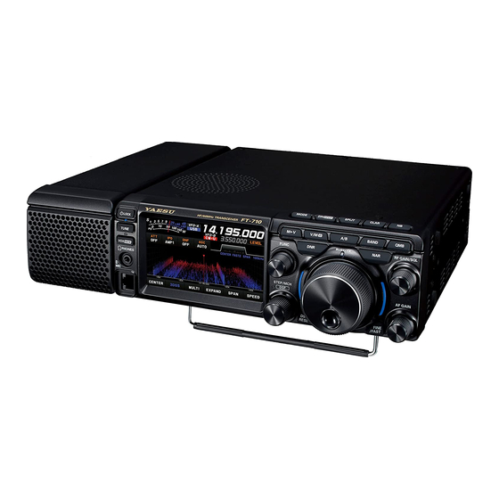
HF/50 MHz TRANSCEIVER
FT-710
Introduction
This manual provides the technical information necessary
for servicing the FT-710 HF/50 MHz TRANSCEIVER.
Servicing this equipment requires expertise in handling
surface-mount chip components. Attempts by non-qualified
persons to service this equipment may result in permanent
damage not covered by the warranty, and may be illegal in
some countries.
While we believe the information in this manual to be cor-
rect, YAESU assumes no liability for damage that may oc-
cur as a result of typographical or other errors that may be
present. Your cooperation in pointing out any inconsisten-
cies in the technical information would be appreciated.
This transceiver was assembled using Pb (lead) free solder, based on the RoHS specification.
Only lead-free solder (Alloy Composition: Sn-3.0Ag-0.5Cu) should be used for repairs performed on this apparatus. The solder stated
above utilizes the alloy composition required for compliance with the lead-free specification, and any solder with the above alloy com-
position may be used.
Technical Supplement
Specifications
Exploded View
Block Diagram
Connection Diagram
Alignment
Board Unit (Schematics, Layouts & Parts)
MAIN Unit
PA Unit
DISPLAY Unit
JACK Unit
Important Note
EH080H90A
©2022 YAESU MUSEN CO., LTD.
Contents
Advertisement

Related Manuals for Yaesu FT-710


Summary of Contents for Yaesu FT-710
- Page 1 While we believe the information in this manual to be cor- Board Unit (Schematics, Layouts & Parts) rect, YAESU assumes no liability for damage that may oc- MAIN Unit cur as a result of typographical or other errors that may be PA Unit present.
- Page 2 9.92lbs (4.5kg) Transmitter 5 - 100 watts (5 - 25W AM carrier) Power Output: J3E (SSB): Balanced, Modulation Types: A3E (AM): Low-Level (Early Stage), F3E (FM): Variable Reactance ±5.0kHz/±2.5kHz (Narrow) Maximum FM Deviation: Better than –50dB (1.8MHz - 29.7MHz Amateur bands) Harmonic Radiation: Better than –63dB (50MHz Amateur band) At least 60dB below peak output SSB Carrier Suppression: Undesired Sideband Suppression: At least 60dB below peak output 3kHz (LSB/USB), 500Hz (CW), 6kHz (AM), 16kHz (FM) Bandwidth: Not more than –6dB from 300 to 2700Hz Audio Response (SSB): 600Ohms (200 to 10kOhms) Microphone Impedance: FT-710 Technical Supplement SPESIFICATIONS -1...
- Page 3 60dB or better (50MHz Amateur band) 2.5 W into 4Ohms with 10% THD Maximum Audio Output: 4 to 16Ohms (4Ohms: nominal) Audio Output Impedance: Less than 4nW Conducted Radiation: Specifications are subject to change, in the interest of technical improvement, without notice or obligation, and are guaranteed only within the amateur bands. FT-710 Technical Supplement SPESIFICATIONS -2...
- Page 4 BIND HEAD TAPTITE-B M2X5(3) KNOB MAIN ASSY U24208007 BIND HEAD TAPTITE-B M2.6X8B U24205001 BIND HEAD TAPTITE-B M2.6X5 RA6358900 U34308001 FLAT HEAD TAPTITE-B M3X8 RUBBER RING (MAIN) Non-designated parts are available only as part of a designated assembly. EXPLODED VIEW -1 FT-710 Technical Supplement...
- Page 5 DISPLAY PANEL P1091158C RA6443100 CONNECTOR RA602540A PORON SHEET (10x115) RA6443100 R0145630 STAND RA6468600 RA6334300 GASKET (2530) ThermalConductivePad RA6396000 CHASSIS R3100700B FOOT RA6443100 CQ1350001 BOTTOM-CASE-ASSY RA6401200 BOTTOM CASE RA602540A RA6119900 GASKET (6x6x12) PORON SHEET (10x115) RA6443100 EXPLODED VIEW -2 FT-710 Technical Supplement...
- Page 6 Block Diagram BLOCK DIAGRAM -1 FT-710 Technical Supplement...
- Page 7 Connection Diagram CONNECTION DIAGRAM -1 FT-710 Technical Supplement...
- Page 8 AF Signal Generator Spectrum Analyzer good to at least 1GHz. Frequency Counter SINAD Meter RF Millivoltmeter DC Voltmeter DC Ammeter (30A) 16-Ohm Dummy Load (100 watts) 50-Ohm Dummy Load (100 watts) 100-Ohm Dummy Load (200 watts) 150-Ohm Dummy Load (100 watts) In-Line Wattmeter (150 watts, 50-Ohm) 4-Ohm AF Dummy Load (3 watts) 1/4-inch 3-contact Plug Important Notice Do not adjust the alignment menus that are not mentioned in thismAnual. FT-710 Technical Supplement ALIGNMENT -1...
- Page 9 Rotate the [STEP/MCH (DSP)] knob so that themAIN Unit. the frequency counter reading is “250.000000 Press and hold in the [BAND], [QMB] and ±20Hz”. Press and hold the [FUNC] knob to save the [NAR] keys, while turning the radio ON, to en- ter the alignment mode. new setting. Rotate the [FUNC] knob to select the alignment parameter “003 [GN] REF FREQ”. TP1005 FT-710 Technical Supplement ALIGNMENT -2...
- Page 10 10dBµV 14.200MHz 029 [RX] IF-AGC 14 14.200MHz 10dBµV 21.200MHz 030 [RX] IF-AGC 21 21.200MHz -2.0dB ± 0.5dB 10dBµV 28.100MHz 031 [RX] IF-AGC 28 28.100MHz 10dBµV 50.500MHz 032 [RX] IF-AGC 50 50.500MHz 10dBµV Press and hold in the [FUNC] knob to save the new setting. FT-710 Technical Supplement ALIGNMENT -3...
- Page 11 Rotate the [FUNC] knob to select the alignment parameter “047 [RX] FM SQL THN”. Press the [STEP/MCH (DSP)] knob. Set the RF Signal Generator to 0dBµV at the 51.500MHz of a 1kHz ±3.5kHz deviation FM modulation audio signal. Rotate the [FUNC] knob to select the alignment parameter “048 [RX] FM SQL TI”. Press the [STEP/MCH (DSP)] knob. Press and hold in the [FUNC] knob to save the new setting. FT-710 Technical Supplement ALIGNMENT -4...
- Page 12 Press and hold the PTT switch then adjust the [STEP/MCH (DSP)] knob so that the DC amme- ter reading is “100mA (±10mA)”. Release the PTT switch. Rotate the [FUNC] knob to select the alignment parameter “056 [TX] VHF PREDR-BIAS”. Press and hold the PTT switch then adjust the [STEP/MCH (DSP)] knob so that the DC amme- ter reading is “100mA (±10mA)”. Release the PTT switch. J4001 J4004 J4005 FT-710 Technical Supplement ALIGNMENT -5...
- Page 13 Press and hold the PTT switch then adjust the [STEP/MCH (DSP)] knob so that the DC am- meter reading is “1.5 A (±150mA)” (European Version: “1.0 A (±150mA)”). Release the PTT switch. Press and hold in the [FUNC] knob to save the new setting. Termination Turn OFF the transceiver. Disconnect the 50-Ohm resistors from J4001, then connect the coaxial cables to J4001. Re-connect the jumper plugs to J4004 and J4005. FT-710 Technical Supplement ALIGNMENT -6...
- Page 14 Perform the same procedures for the Alignment Press and hold in the [FUNC] knob to save the parameter “085 [TX] 100W FALC 3.5” through new setting. “219 [TX] 5W TXG 50” (UK version: “234 [TX] 5W TXG 70”) as indicated by the chart on the next page. Press and hold in the [FUNC] knob to save the new setting. FT-710 Technical Supplement ALIGNMENT -7...
- Page 15 Maximum deflection 5W (+1W/-0W) 5W (+1W/-0W) Maximum deflection Maximum deflection 101W (+5W/-1W) Maximum deflection 50W (+5W/-0W) Maximum deflection Rotate the 20W (+2W/-0W) [STEP/MCH Maximum deflection (DSP)] knob 10W (+1W/-0W) Maximum deflection 5W (+1W/-0W) Maximum deflection FT-710 Technical Supplement ALIGNMENT -8...
- Page 16 244 [TX] REV ALC 50 UK version only Connect the 16.6-Ohm Dummy Load to the ANT jack. Rotate the [FUNC] knob to select the align- ment parameter “245 [TX] REV ALC 70”. Key the transmitter, then rotate the [STEP/ MCH (DSP)] knob so that the PO meter (on the front panel) reading is 25 W (+0 W/-10 Unkey the transmitter. Press and hold in the [FUNC] knob to save the new setting. FT-710 Technical Supplement ALIGNMENT -9...
- Page 17 MAIN Unit Circuit Diagram (MAIN Unit/CNTL) FT-710 Technical Supplement MAIN -1...
- Page 18 MAIN Unit Circuit Diagram (MAIN Unit/DVI) FT-710 Technical Supplement MAIN -2...
- Page 19 MAIN Unit Circuit Diagram (MAIN Unit/DSP) FT-710 Technical Supplement MAIN -3...
- Page 20 MAIN Unit Circuit Diagram (MAIN Unit/AF) FT-710 Technical Supplement MAIN -4...
- Page 21 MAIN Unit Circuit Diagram (MAIN Unit/RX) FT-710 Technical Supplement MAIN -5...
- Page 22 MAIN Unit Parts Layout (side A) FT-710 Technical Supplement MAIN -6...
- Page 23 MAIN Unit Parts Layout (side B) FT-710 Technical Supplement MAIN -7...
- Page 24 GRM155R61E105KE11D K22149010 C 1098 CHIP TA.CAP. TMCSA1C105MTRF K78120009 C 1099 CHIP CAP. GRM1553C1H3R0BA01D K22178290 C 1100 CHIP CAP. 0.1uF GRM155R71H104KE14D K22178872 C 1101 CHIP CAP. 0.001uF GRM155B11H102KA01D K22178809 C 1102 CHIP CAP. 0.01uF GRM155R71H103KA88D K22178848 FT-710 Technical Supplement MAIN -8...
- Page 25 C 2009 CHIP CAP. 10pF GRM1552C1H100JA01D K22178212 C 2011 CHIP CAP. 10uF GRM188B31A106ME69D K22104810 C 2013 CHIP CAP. 10uF GRM188B31A106ME69D K22104810 C 2014 CHIP CAP. 0.1uF GRM155R71H104KE14D K22178872 C 2016 CHIP CAP. 10uF GRM188B31A106ME69D K22104810 FT-710 Technical Supplement MAIN -9...
- Page 26 C 2196 CHIP CAP. 220pF GRM1552C1H221JA01D K22179713 C 2197 CHIP CAP. 220pF GRM1552C1H221JA01D K22179713 C 2198 CHIP CAP. 220pF GRM1552C1H221JA01D K22179713 C 2601 CHIP CAP. 0.001uF GRM155B11H102KA01D K22178809 C 2602 CHIP CAP. 0.01uF GRM155R71H103KA88D K22178848 FT-710 Technical Supplement MAIN -10...
- Page 27 C 2696 CHIP CAP. 0.1uF GRM155R71H104KE14D K22178872 C 2697 CHIP CAP. 0.1uF GRM155R71H104KE14D K22178872 C 2698 CHIP CAP. 22uF GRM21BR61E226ME44L K22140830 C 2699 CHIP CAP. 0.01uF GRM155R71H103KA88D K22178848 C 2700 CHIP CAP. 0.1uF GRM155R71H104KE14D K22178872 FT-710 Technical Supplement MAIN -11...
- Page 28 C 3032 CHIP CAP. 0.1uF GRM155R71H104KE14D K22178872 C 3033 CHIP CAP. 0.1uF GRM155R71H104KE14D K22178872 C 3034 CHIP CAP. 0.01uF GRM155R71H103KA88D K22178848 C 3035 CHIP CAP. 0.01uF GRM155R71H103KA88D K22178848 C 3036 CHIP CAP. 0.01uF GRM155R71H103KA88D K22178848 FT-710 Technical Supplement MAIN -12...
- Page 29 C 3110 CHIP CAP. 33pF GRM1552C1H330JA01D K22178224 C 3111 CHIP CAP. 22pF GRM1552C1H220JA01D K22178220 C 3112 CHIP CAP. 68pF GRM1552C1H680JA01D K22178232 C 3113 CHIP CAP. 47pF GRM1552C1H470JA01D K22178228 C 3114 CHIP CAP. 15pF GRM1552C1H150JA01D K22178216 FT-710 Technical Supplement MAIN -13...
- Page 30 K22178872 C 3187 CHIP CAP. 0.1uF GRM155R71H104KE14D K22178872 C 3188 CHIP CAP. GRM155R61E105KE11D K22149010 C 3189 CHIP CAP. 0.01uF GRM155R71H103KA88D K22178848 C 3190 CHIP CAP. 0.01uF GRM155R71H103KA88D K22178848 C 3191 CHIP CAP. 0.01uF GRM155R71H103KA88D K22178848 FT-710 Technical Supplement MAIN -14...
- Page 31 C 3264 CHIP CAP. 0.1uF GRM155R71H104KE14D K22178872 C 3265 CHIP CAP. 0.01uF GRM155R71H103KA88D K22178848 C 3266 CHIP CAP. 0.1uF GRM155R71H104KE14D K22178872 C 3267 CHIP CAP. 0.01uF GRM155R71H103KA88D K22178848 C 3268 CHIP CAP. 0.1uF GRM155R71H104KE14D K22178872 FT-710 Technical Supplement MAIN -15...
- Page 32 C 3386 CHIP CAP. 18pF GRM1552C1H180JA01D K22178218 C 3386 CHIP CAP. 15pF GRM1552C1H150JA01D K22178216 C 3387 CHIP CAP. 100pF GRM1552C1H101JA01D K22178236 C 3389 CHIP CAP. 33pF GRM1552C1H330JA01D K22178224 C 3391 CHIP CAP. 330pF GRM1555C1H331JA01D K22179744 FT-710 Technical Supplement MAIN -16...
- Page 33 UDZS TE-17 6.8B G2070888 D 1025 DIODE BAS316 G2070716 D 1026 DIODE BAS316 G2070716 D 1800 DIODE RB160M-30TR G2071100 D 1801 DIODE ARRAY DRTR5V0U2SO-7 G2090861 D 2001 DIODE BAS316 G2070716 D 2604 DIODE ARRAY DRTR5V0U2SO-7 G2090861 FT-710 Technical Supplement MAIN -17...
- Page 34 FB2607 FERRITE BEADS BLM15BD102SN1D L9190133 FB3001 FERRITE BEADS BLM18AG601SN1D L9190111 FB3002 FERRITE BEADS BLM18AG601SN1D L9190111 FB3004 FERRITE BEADS BLM18AG601SN1D L9190111 FB3007 FERRITE BEADS BLM18AG601SN1D L9190111 J 1001 CONNECTOR SC25-12WS P0090631 J 1002 CONNECTOR 24FLT-SM2-TB(LF)(SN)(M) P1091128 FT-710 Technical Supplement MAIN -18...
- Page 35 0.47uH 1008CS-471XGLC L1691678 L 3032 M.RFC 0.27uH 1008CS-271XGLC L1691675 L 3033 M.RFC 0.18uH 1008CS-181XGLC L1691673 L 3034 M.RFC 0.15uH 1008CS-151XGLC L1691672 L 3035 CHIP COIL 0.15uH C2520C-R15G-RA L1691296 L 3036 CHIP COIL 0.15uH C2520C-R15G-RA L1691296 FT-710 Technical Supplement MAIN -19...
- Page 36 G3070298 Q 1026 TRANSISTOR DTC114EUA T106 G3070084 Q 1027 RRR030P03 G3070448 Q 1028 NJM2835DL1-33-TE1 G1095324 Q 1029 MP5073GG G1095792 Q 1030 TRANSISTOR DTC114YUA T106 G3070298 Q 1031 74VHCT125AFT(BE) G1095220 Q 1032 TRANSISTOR DTC124TU T106 G3070065 FT-710 Technical Supplement MAIN -20...
- Page 37 DTC114EUA T106 G3070084 Q 3024 TRANSISTOR DTC114EUA T106 G3070084 Q 3025 TRANSISTOR 55GN01CA-TB-E G3070550 Q 3026 TRANSISTOR UMD5N TR G3070343 Q 3027 TRANSISTOR 55GN01CA-TB-E G3070550 Q 3028 TRANSISTOR MMG3H21NT1 G3070563 Q 3029 TRANSISTOR DTC114EUA T106 G3070084 FT-710 Technical Supplement MAIN -21...
- Page 38 RMC1/16S 472JTH J24189033 R 1084 CHIP RES. 1/16W RMC1/16S 103JTH J24189037 R 1085 CHIP RES. 1/16W RMC1/16S 103JTH J24189037 R 1087 CHIP RES. 1/16W RMC1/16S 103JTH J24189037 R 1088 CHIP RES. 1/16W RMC1/16S JPTH J24189070 FT-710 Technical Supplement MAIN -22...
- Page 39 RMC1/16S 472JTH J24189033 R 1825 CHIP RES. 1/16W RMC1/16S JPTH J24189070 R 1826 CHIP RES. 1/16W RMC1/16S JPTH J24189070 R 1827 CHIP RES. 1/16W RMC1/16S 821JTH J24189024 R 1829 CHIP RES. 1/16W RMC1/16S 103JTH J24189037 FT-710 Technical Supplement MAIN -23...
- Page 40 1/16W RMC1/16S 102JTH J24189025 R 2106 CHIP RES. 1/16W RMC1/16S JPTH J24189070 R 2108 CHIP RES. 1/16W RMC1/16S 103JTH J24189037 R 2109 CHIP RES. 1/16W RMC1/16S JPTH J24189070 R 2110 CHIP RES. 1/16W RMC1/16SK473FTH J24189525 FT-710 Technical Supplement MAIN -24...
- Page 41 RMC1/16S 153JTH J24189039 R 2656 CHIP RES. 1/16W RMC1/16S 823JTH J24189048 R 2657 CHIP RES. 1/16W RMC1/16S 273JTH J24189042 R 2658 CHIP RES. 1/16W RMC1/16S JPTH J24189070 R 2659 CHIP RES. 1/16W RMC1/16S JPTH J24189070 FT-710 Technical Supplement MAIN -25...
- Page 42 RMC1/16S 823JTH J24189048 R 2737 CHIP RES. 220k 1/16W RMC1/16S 224JTH J24189053 R 2738 CHIP RES. 1/16W RMC1/16S 123JTH J24189038 R 2739 CHIP RES. 1/16W RMC1/16S 273JTH J24189042 R 2740 CHIP RES. 1/16W RMC1/16S JPTH J24189070 FT-710 Technical Supplement MAIN -26...
- Page 43 RMC1/16S 330JTH J24189007 R 3022 CHIP RES. 1/2W RMC1/2 560JTE J24275560 R 3023 CHIP RES. 1/4W RMC1/4 151JATP J24245151 R 3024 CHIP RES. 1/16W RMC1/16S 103JTH J24189037 R 3025 CHIP RES. 1/16W RMC1/16S 101JTH J24189013 FT-710 Technical Supplement MAIN -27...
- Page 44 RMC1/16S 330JTH J24189007 R 3097 CHIP RES. 1/16W RMC1/16S 471JTH J24189021 R 3098 CHIP RES. 1.8k 1/16W RMC1/16S 182JTH J24189028 R 3099 CHIP RES. 1/16W RMC1/16S 100JTH J24189001 R 3100 CHIP RES. 1/16W RMC1/16S JPTH J24189070 FT-710 Technical Supplement MAIN -28...
- Page 45 RELAY DC12V FTR-B4SA012Z-B05 M1190209 RL3001 RELAY DC12V FTR-B4SA012Z-B05 M1190209 RL3002 RELAY DC12V FTR-B4SA012Z-B05 M1190209 RL3003 RELAY DC12V FTR-B4SA012Z-B05 M1190209 RL3004 RELAY DC12V FTR-B4SA012Z-B05 M1190209 S 1001 SLIDE SWITCH SSSS820201 N6090107 SC1001 SHIELD CASE VCO RA1360000 FT-710 Technical Supplement MAIN -29...
- Page 46 Q5000103 X 1001 XTAL DSX321G 24MHz DSX321G 24.000MHZ H0103444 X 1002 VCTCXO 35.7142MHz DSA211SDN-35.7142MHz H9501965 X 1801 XTAL DSX321G 24MHz DSX321G 24.000MHZ H0103444 X 2601 XTAL DSX321G 24MHz DSX321G 24.000MHZ H0103444 SHIELD CASE (35X120) RA6430800 FT-710 Technical Supplement MAIN -30...
- Page 47 PA Unit Circuit Diagram FT-710 Technical Supplement PA -1...
- Page 48 PA Unit Parts Layout (side A) FT-710 Technical Supplement PA -2...
- Page 49 PA Unit Parts Layout (side B) FT-710 Technical Supplement PA -3...
- Page 50 C 4127 CHIP CAP. 0.001uF GRM155B11H102KA01D K22178809 C 4128 CHIP CAP. 0.1uF GRM155R71H104KE14D K22178872 C 4129 CHIP CAP. 0.001uF GRM155B11H102KA01D K22178809 C 4134 CHIP CAP. 0.01uF GRM155R71H103KA88D K22178848 C 4135 CHIP CAP. 0.001uF GRM155B11H102KA01D K22178809 FT-710 Technical Supplement PA -4...
- Page 51 K22240329 C 4273 AL.ELECTRO.CAP. 1000uF SK025M102G20SR K40149088 C 4274 CHIP CAP. 0.01uF GRM155R71H103KA88D K22178848 C 4275 CHIP CAP. 0.1uF GRM155B31E104KA87D K22148838 C 4276 CHIP CAP. 0.1uF 250V GRM31CR72E104KW03L K22241804 C 4277 AL.ELECTRO.CAP. 47uF RE2-25V470ME3#-T2 K46140004 FT-710 Technical Supplement PA -5...
- Page 52 C 4381 CHIP CAP. 82pF 500V GQM22M5C2H820JB01L K22273274 W/ CE C 4381 CHIP CAP. 100pF 500V GQM22M5C2H101JB01L K22273276 W/O CE C 4382 CHIP CAP. 390pF 630V GRM31A5C2J391JW01D K22281239 C 4383 CHIP CAP. 220pF 630V GRM31A5C2J221JW01D K22281236 FT-710 Technical Supplement PA -6...
- Page 53 C 4470 CHIP CAP. 0.01uF GRM155R71H103KA88D K22178848 C 4471 CHIP CAP. 0.01uF GRM155R71H103KA88D K22178848 C 4472 CERAMIC CAP. 39pF CC45SL3FD390JYNNA K00359033 C 4473 CERAMIC CAP. 39pF CC45SL3FD390JYNNA K00359033 C 4474 CERAMIC CAP. 39pF CC45SL3FD390JYNNA K00359033 FT-710 Technical Supplement PA -7...
- Page 54 C 4562 CHIP CAP. 0.01uF GRM155R71H103KA88D K22178848 C 4563 CHIP CAP. 0.1uF GRM155R71H104KE14D K22178872 C 4564 CHIP CAP. 0.01uF GRM155R71H103KA88D K22178848 C 4565 CHIP CAP. 0.1uF GRM155R71H104KE14D K22178872 C 4566 CHIP CAP. 22pF GRM1552C1H220JA01D K22178220 FT-710 Technical Supplement PA -8...
- Page 55 FERRITE BEADS BLM15BD182SN1D L9190220 FB4002 FERRITE BEADS BLM15BD182SN1D L9190220 FB4003 FERRITE BEADS BLM15BD182SN1D L9190220 FB4004 FERRITE BEADS FBMH3225HM102NT L9190173 FB4005 RFC WITH BEADS 3A RI5.8X6.4-2 L1020732 HS4001 HEATSINK PLATE (7X2.5) RA6086800 HS4002 HEATSINK PLATE RA6299900 FT-710 Technical Supplement PA -9...
- Page 56 TRANSISTOR DTC144EUA T106 G3070041 Q 4011 RD04HMS2 G3090176 Q 4012 TRANSISTOR DTC144EUA T106 G3070041 Q 4013 TRANSISTOR 2SA1576A T106 R G3115768R Q 4014 LM2902PWR G1094009 Q 4015 TRANSISTOR DTC114EUA T106 G3070084 Q 4017 LM2902PWR G1094009 FT-710 Technical Supplement PA -10...
- Page 57 RMC1/16 473JATP J24185473 R 4016 CHIP RES. 1/16W RMC1/16 121JATP J24185121 R 4018 CHIP RES. 1/16W RMC1/16 101JATP J24185101 R 4020 CHIP RES. 1/16W RMC1/16 470JATP J24185470 R 4021 CHIP RES. 1/16W RMC1/16 101JATP J24185101 FT-710 Technical Supplement PA -11...
- Page 58 1/16W RMC1/16 104FTP J24183104 R 4110 CHIP RES. RMC1 220JTE J24305220 R 4114 CHIP RES. 1/16W RMC1/16 333FTP J24183333 R 4119 CHIP RES. 1/16W RMC1/16 102JATP J24185102 R 4120 CHIP RES. 1/16W RMC1/16 333JATP J24185333 FT-710 Technical Supplement PA -12...
- Page 59 RMC1/16 101JATP J24185101 R 4205 CHIP RES. 1/16W RMC1/16 220JATP J24185220 R 4206 CHIP RES. 1/16W RMC1/16 101JATP J24185101 R 4207 CHIP RES. 1/16W RMC1/16 101JATP J24185101 R 4208 CHIP RES. 1/16W RMC1/16 101JATP J24185101 FT-710 Technical Supplement PA -13...
- Page 60 FTR-F3AA012E-(F) M1190224 RL4025 RELAY FTR-F3AA012E-(F) M1190224 RL4026 RELAY FTR-F3AA012E-(F) M1190224 RL4027 RELAY DC12V FTR-B4SA012Z-B05 M1190209 RL4028 RELAY FTR-F3AA012E-(F) M1190224 RL4029 RELAY FTR-F3AA012E-(F) M1190224 RL4030 RELAY FTR-F3AA012E-(F) M1190224 RL4031 RELAY FTR-F3AA012E-(F) M1190224 RL4032 RELAY FTR-F3AA012E-(F) M1190224 FT-710 Technical Supplement PA -14...
- Page 61 T 4004 COIL PWR-WIDE D12A-RID16X32X32 L0023360 TC4001 TRIMMER CAP. 20pF KKT320TR K91000294 TH4001 THERMISTOR ERTJ0ER103J G9090119 TH4003 THERMISTOR NCP18XV103J03RB G9090179 Y 4001 CORE 3A5 RIB-10X20X10 L9190101 SHIELD CASE (19x25) RA6068800 W/ CE TUBE (SI) RA1179900 FT-710 Technical Supplement PA -15...
- Page 62 DISPLAY Unit Circuit Diagram FT-710 Technical Supplement DISPLAY -1...
- Page 63 DISPLAY Unit Parts Layout side A side B FT-710 Technical Supplement DISPLAY -2...
- Page 64 C 6090 CHIP CAP. 47pF GRM1552C1H470JA01D K22178228 C 6091 CHIP CAP. 22uF GRM21BR61E226ME44L K22140830 C 6092 CHIP CAP. 22uF GRM21BR61E226ME44L K22140830 C 6093 CHIP CAP. 0.1uF GRM155R71H104KE14D K22178872 C 6094 CHIP CAP. 0.1uF GRM155R71H104KE14D K22178872 FT-710 Technical Supplement DISPLAY -3...
- Page 65 K22178809 C 6176 CHIP CAP. 0.1uF GRM155B11A104KA01D K22108802 C 6180 CHIP CAP. 0.1uF GRM155R71H104KE14D K22178872 C 6182 CHIP CAP. GRM155R61E105KE11D K22149010 C 6184 CHIP CAP. 0.01uF GRM155R71H103KA88D K22178848 C 6187 CHIP CAP. 0.1uF GRM155R71H104KE14D K22178872 FT-710 Technical Supplement DISPLAY -4...
- Page 66 L1692236 L 6004 CHIP COIL 2.2uH SWRH5D28S-2R2NT L1692236 L 6005 CHIP COIL 4.7uH SWRH2D18R-4R7NT L1692235 L 6006 CHIP COIL 2.2uH SWRH5D28S-2R2NT L1692236 L 6007 CHIP COIL 2.2uH SWRH5D28S-2R2NT L1692236 Q 6001 TRANSISTOR DTC114YUA T106 G3070298 FT-710 Technical Supplement DISPLAY -5...
- Page 67 RMC1/16S 102JTH J24189025 R 6045 CHIP RES. 1/16W RMC1/16S 330JTH J24189007 R 6046 CHIP RES. 1/16W RMC1/16S 330JTH J24189007 R 6047 CHIP RES. 1/16W RMC1/16S 330JTH J24189007 R 6048 CHIP RES. 1/16W RMC1/16S 330JTH J24189007 FT-710 Technical Supplement DISPLAY -6...
- Page 68 CHIP RES. 1/16W RMC1/16S 103JTH J24189037 R 6137 CHIP RES. 1/16W RMC1/16S 103JTH J24189037 R 6138 CHIP RES. 1/16W RMC1/16S 473JTH J24189045 R 6139 CHIP RES. 1/16W RMC1/16SK101FTH J24189504 R 6140 CHIP RES. 1/16W RMC1/16SK101FTH J24189504 FT-710 Technical Supplement DISPLAY -7...
- Page 69 RMC1/16S 103JTH J24189037 R 6216 CHIP RES. 1/16W RMC1/16S 103JTH J24189037 R 6218 CHIP RES. 1/16W RMC1/16S 103JTH J24189037 R 6219 CHIP RES. 1/16W RMC1/16S 103JTH J24189037 R 6221 CHIP RES. 1/16W RMC1/16S 473JTH J24189045 FT-710 Technical Supplement DISPLAY -8...
- Page 70 S 6015 TACTILE SWITCH EVQP2R02W N5090175 S 6016 TACTILE SWITCH EVQP2R02W N5090175 S 6017 TACTILE SWITCH EVQP2R02W N5090175 S 6018 ROTARY ENCODER EC12D1564402 Q9001070 S 6019 ROTARY ENCODER EC12D1564402 Q9001070 SC6001 SHIELD CASE (13X18) RA6420400 FT-710 Technical Supplement DISPLAY -9...
- Page 71 VR6002 POT. RK09D1130C2P 10KB J60800268 X 6001 XTAL DSX321G 48MHz 48.000MHZ H0103486 X 6002 XTAL DSX321G 27MHz 27.000MHZ H0103484 X 6003 XTAL SC-32S 32.768kHz SC-32S 32.768KHZ H0103464 X 6004 XTAL DSX321G 12MHz DSX321G 12.000MHZ H0103442 FT-710 Technical Supplement DISPLAY -10...
- Page 72 JACK Unit Circuit Diagram FT-710 Technical Supplement JACK -1...
- Page 73 JACK Unit Parts Layout side A side B FT-710 Technical Supplement JACK -2...
- Page 74 RMC1/4 101JATP J24245101 R 7012 CHIP RES. 1/16W RMC1/16S JPTH J24189070 R 7013 CHIP RES. 1/16W RMC1/16S JPTH J24189070 R 7014 CHIP RES. 1/10W RMC1/10T 000J J24205000 R 7015 CHIP RES. 1/16W RMC1/16S JPTH J24189070 FT-710 Technical Supplement JACK -3...
- Page 75 Copyright 2022 YAESU MUSEN CO., LTD. All rights reserved. No portion of this manual may be reproduced without the permission of YAESU MUSEN CO., LTD. YAESU MUSEN CO., LTD. Tennozu Parkside Building 2-5-8 Higashi-Shinagawa, Shinagawa-ku, Tokyo 140-0002 Japan YAESU USA 6125 Phyllis Drive, Cypress, CA 90630, U.S.A.
Need help?
Do you have a question about the FT-710 and is the answer not in the manual?
Questions and answers
what is the cable that goes from ft-710 to fl700 amplifier
The Yaesu FT-710 requires the "CT-58" Band Data Cable and the "CT-58" ALC Cable to connect to the FL-700 amplifier.
This answer is automatically generated