Advertisement
Quick Links
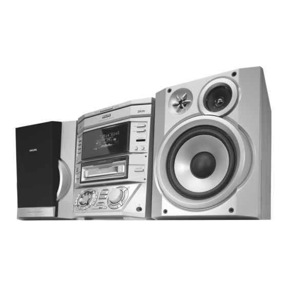
CDR Mini System
SERVICING
For servicing FW-R8, the set can be divided into two parts:
1. Except for the CD-R/W module the set has to be repaired on component level.
2. The CD-R/W module will be exchanged completely in case of a failure.
The defective CD-R/W module has to be returned for central repair.
Available circuit descriptions: The Basics of Compact Disc Recordable/Rewritable
Table of Contents
Location of printed circuit boards . . . . . . . . . . . . . . . . . . . 1-2
Technical specification . . . . . . . . . . . . . . . . . . . . . . . . . . . 2-1
Measurement setup . . . . . . . . . . . . . . . . . . . . . . . . . . . . . 2-2
RC-5 codes. . . . . . . . . . . . . . . . . . . . . . . . . . . . . . . . . . . . 2-3
Brief operating instructions . . . . . . . . . . . . . . . . . . . . . . . . 2-4
Warnings & safety . . . . . . . . . . . . . . . . . . . . . . . . . . . . . . 3-1
Service Testprogram . . . . . . . . . . . . . . . . . . . . . . . . . . . . 3-3
Wiring Diagram . . . . . . . . . . . . . . . . . . . . . . . . . . . . . . . . . 4-1
Block/Leveldiagram . . . . . . . . . . . . . . . . . . . . . . . . . . . . . 5-1
Front Board . . . . . . . . . . . . . . . . . . . . . . . . . . . . . . . . . . . . 6
Tuner Board . . . . . . . . . . . . . . . . . . . . . . . . . . . . . . . . . . . . 7
Audio Frequency Board (AF7) . . . . . . . . . . . . . . . . . . . . . 8
©
Copyright 2000 Philips Consumer Electronics B.V. Eindhoven, The Netherlands
All rights reserved. No part of this publication may be reproduced, stored in a retrieval
system or transmitted, in any form or by any means, electronic, mechanical, photocopying,
or otherwise without the prior permission of Philips.
Published by HB 0015 Service Audio
3rd generation Compact Disc Recording
Printed in The Netherlands
Subject to modification
4822 725 25242
3104 125 40100
Power Board. . . . . . . . . . . . . . . . . . . . . . . . . . . . . . . . . . . . 9
3 Disc Changer Module . . . . . . . . . . . . . . . . . . . . . . . . . . 10
CD R/W Module . . . . . . . . . . . . . . . . . . . . . . . . . . . . . . . . 11
Exploded view of set. . . . . . . . . . . . . . . . . . . . . . . . . . . . 12-1
Partslist of set . . . . . . . . . . . . . . . . . . . . . . . . . . . . . . . . . 12-3
FW-R8
/17/21/22
CLASS 1
LASER PRODUCT
©
3103 785 25040
Advertisement

Subscribe to Our Youtube Channel
Related Manuals for Philips FW-R8/17


Summary of Contents for Philips FW-R8/17
- Page 1 LASER PRODUCT © Copyright 2000 Philips Consumer Electronics B.V. Eindhoven, The Netherlands All rights reserved. No part of this publication may be reproduced, stored in a retrieval system or transmitted, in any form or by any means, electronic, mechanical, photocopying, or otherwise without the prior permission of Philips.
- Page 2 Location of Printed Circuit Boards Location of PCB R8 2000 02 14...
- Page 3 Technical Specification General: CDC unit: Mains voltage : 120 / 240V switchable Frequency response within : 20Hz - 20kHz at ±3dB (for /21) : 230V Signal/Noise ratio : > 94dB (A-weighted) (for /22) : 120V Distortion at 1kHz,0dB : -90dB (for /37) Mains frequency : 50 ~ 60Hz...
- Page 4 Measurement Setup Bandpass Tuner SW LF Voltmeter 250Hz-15kHz Aerial replacement e.g. PM2534 e.g. 7122 707 48001 RF Generator Capacitor e.g. PM5326 S/N and distortion meter e.g. Sound Technology ST1700B To avoid atmospheric interference all AM-measurements have to be carried out in a Faraday´s cage. Use a bandpass filter (or at least a high pass filter with 250Hz) to eliminate hum (50Hz, 100Hz).
- Page 5 RC5 Codes Remote control key System Code Command Code Remote control key System Code Command Code Standby 17,20, 21, 26 ALARM SLEEP BRIGHTNESS REPEAT 20, 26 SHUFFLE 20, 26 Tuner TRACK INCREMENT VOLUME + 1(ABC) 17,20, 21, 26 VOLUME - 2 (DEF) 17,20, 21, 26 20, 26...
- Page 6 CONTROLS AND CONNECTIONS CONTROLS AND CONNECTIONS On the front 0 Source selection ¡ FINALIZE.......finalizes and unfinalizes CD 1, CD 2, CD 3 ....selects the CD changer, recordings switches to CD 1, CD 2 or ™ REC TYPE......enters/exits the recording & CD 3 menu £...
- Page 7 INSTALLATION INSTALLATION Power Antenna connections The type plate is located on the rear of the unit. AM antenna The supplied loop antenna is for indoor use only. 1 Check whether the power voltage as shown on the type plate corresponds to your local power voltage. If it does 1 Fit the plug of the loop antenna to AM AERIAL as shown not, consult your dealer or service organization.
- Page 8 REMOTE CONTROL DISPLAY CD Recorder Remote control buttons Display ..current program is being recorded with COMPILE CDC 2 ......switches the unit to standby The display of the unit is divided into 3 sections, which show high speed dubbing and auto finalize you the following: ..FM station is being recorded CDR, TUNER, CD1,...
- Page 9 BASIC FUNCTIONS BASIC FUNCTIONS LOUDNESS 3 CD changer: • Press LOUDNESS to switch loudness either on or off. Press OPEN/CLOSE on the unit again to close the tray. is shown and Loudness is displayed if LOUDNESS The tray is closed and Reading is displayed. G E R loudness is on.
- Page 10 BASIC FUNCTIONS PROGRAM Playing tracks in random order Selecting a disc on the CD changer Erasing a track from the program 1 Press SHUFFLE on the remote control during playback. is shown and either all tracks of the program or 1 If necessary, press Ç...
- Page 11 ABOUT RECORDING INTERNAL RECORDING High speed recording and automatic finalizing Basic information Direct Line Recording (DLR) Recording modes (optional) of the current program The CD recorder deck offers you 3 main functions: The CD recorder is equipped with the high-performance Direct For internal recordings you can record from the internal 1 Make sure the CDR(W) is absolutely free of scratches and –...
- Page 12 INTERNAL RECORDING INTERNAL RECORDING 5 Press YES to confirm your selection. 4 Press CD 1, CD 2 or CD 3 to select the disc with which you ANALO G ANALO G DIGITA L / DIGITA L / Both decks will be selected in the display, the arrow wish to mix the microphone.
- Page 13 EXTERNAL RECORDING EXTERNAL RECORDING 6 Start playback on the selected source. 4 Repeatedly press DIGITAL / ANALOG AUX to select the Manual recording DIGITA L / ANALO G The CD recorder starts to record simultaneously and input for the external source with which you wish to mix Manual recording from an external source is shown.
- Page 14 EXTERNAL RECORDING (UN)FINALIZING, ERASING (UN)FINALIZING, ERASING 5 Press YES to confirm your selection. Automatic track increment Unfinalizing CDRW discs Erase?, the total playing time and the total number of In recording mode, tracks will be incremented automatically so If you want to record (or erase) on (from) a finalized CDRW, tracks to be erased are displayed.
- Page 15 FEATURES FEATURES Storing text during recording Erasing text Track editing (on CD changer only) You can store and edit text even while recording a single 1 Press EDIT TEXT to enter the text edit menu. is blinking, Text Edit is displayed. You can create a “track”...
- Page 16 TUNER CLOCK/TIMER 2 Keep PROG (PROGRAM on the remote control) pressed for ANALO G ANALO G DIGITA L / DIGITA L / more than 2 seconds. Autoprogram is displayed, and the current STANDBY PROG STANDBY TUNE R TUNE R preset number in the music calendar start blinking. iR SEN iR SEN CD 1...
- Page 17 CLOCK/TIMER TECHNICAL DATA You can select different timer functions which will be activated 5 Use à SEARCH or á SEARCH on the unit to move from Subject to modification without notice. Speakers at a chosen time. Make sure the clock is set before using one hour to minutes of start of recording.
- Page 18 2-16 Brief Operating Instructions TROUBLESHOOTING If you are unable to solve a problem by following these hints, WARNING consult your dealer or service center. Under no circumstances should you try to repair the LASER SAFETY unit yourself as this will invalidate the guarantee. Do not open the unit as there is a risk of electric shock.
- Page 19 Warnings & Safety © ñ WARNING WAARSCHUWING All ICs and many other semiconductors are susceptible to Alle IC´s en vele andere halfgeleiders zijn gevoelig voor electrostatic discharges (ESD). Careless handling during electrostatische ontladingen (ESD). repair can reduce life drastically. Onzorgvuldig behandelen tijdens reparatie kan de levensduur When repairing, make sure that you are connected with the drastisch doen vermindern.
- Page 20 Service Tools TORX T10 screwdriver with shaftlength 150mm ........4822 395 50423 TORX screwdriver set SBC 163 ..............4822 295 50145 Audio signal disc SBC 429..............4822 397 30184 Playability test disc SBC444 ..............4822 397 30245 Test disc 5 (disc without errors) + Test disc 5A (disc with dropout errors, black spots and fingerprints) SBC 426/426A ..............4822 397 30096 Burn in test disc (65 min.
- Page 21 SERVICE TESTPROGRAM VARIOUS TESTS To enter Service * To leave Service Testprogram plug mains cord off. Testprogram hold STOP & PLAY buttons depressed while plugging mainscord in. Display shows stands for Service mode version number stands for version number of the µP - software. of the software used in the S-FW-R8-VXX front µP.
- Page 22 SERVICE TESTPROGRAM To enter Service * To leave Service Testprogram plug mains cord off. Testprogram hold CDR MODULE PLAY & STOP buttons depressed while plugging mainscord in. Display shows stands for Service mode version number stands for version number of the µP - software. of the software used in the S-FW-R8-VXX front µP.
- Page 23 Wiring Diagram FW-R8 LIGHT GUIDE 3 CDC KEY AMPLIFIER L/R 1538 1104 SW_INFO FRONTBOARD MIC_KILL SRDT SRDT 1525 1526 1527 Power 5 CD_SH_STR MIC_DET DQSY DQSY 8015 ( 280mm ) CD_SH_CLK FW 7/8 R Series LED_CLK UP_CLK UP_CLK FFC 4 p SICL LED_ON D_GND...
- Page 24 Block / Leveldiagram x100 Headphone out CONTROL Nom. 1 mV BASS 0 dB 2800 mV L&R POWER MUTE 1 VOLUME I SOUND VOLUME II SLOW Power Board SOURCE FADER SELECTOR for details see TUNER Ri=100K Chapter 9 Nom. 110 mV 50 dB Part of TDA7437 Part of TDA7437...
- Page 25 1160 B2 4204 C2 1162 B1 4205 B1 Digital switch Board Copperside view 1163 B2 4206 B1 1164 A2 5130 A1 2220 B2 7140 B1 2221 A1 7142 C1 2222 B2 7145 B1 2225 B2 9401 B2 2226 A2 9402 B2 2227 A2 9403 C1 2221...
- Page 26 Blockdiagram 1105 FRONT BOARD (Technical Front) PRESET PRESET STEP STEP TOTAL TOTAL TRACK TRACK TIME TIME TOTAL TRACK TRACK TIME TIME TU CE CD CHANGER CD CHANGER CD CHANGER CD CHANGER CD RECORDER CD RECORDER CD RECORDER CD RECORDER TUNER TUNER TUNER TUNER...
- Page 27 1160 A1 1162-A E9 Digital switch Board 1162-B B9 1160 +5VA DIGI_IO_SW1 1163 C1 5,6V 1164 E1 DIGI_IO_SW0 2220 B3 2221 E8 2222 F5 DIGI_IO_SW0 LOGIC 2225 D2 220R 2226 E1 7142 +2.5VIC 2227 A3 3359 2,5V 2228 E9 FE-ST-VK-N DIG.
- Page 28 2100 B6 2116 C3 2136 A5 2145 A5 2166 C6 2175 C1 2185 A2 2194 A6 3097 A5 3107 A3 3116 A4 3125 A4 3134 A4 3143 B7 3152 B7 3162 B4 3171 B4 3180 A2 3189 B2 3198 B3 3207 B3 3216 C4 3225 A2...
- Page 29 0401 G1 1105 E15 2110 A12 2127 E4 2142 D11 2155 H3 2197 H2 3101 A1 3111 B7 3121 B5 3131 B8 3141 C5 3151 C10 3162 D10 3172 E10 3182 A12 3192 F7 3202 G6 3212 G9 3222 H5 3233 D12 5109 A4 6107 C13...
- Page 30 0042 A3 F427 E10 0043 E3 F478 A3 1111 B6 F479 A3 FRONT BOARD SHEET 2 1113 E4 F480 A3 1114 E4 F481 A3 1115 E4 F482 A3 1116 E5 F483 B3 F484 C6 DATA BUS from Sheet1 1117 E5 0042 1118 E5 F485 B7...
- Page 31 0042 C2 0406 C1 1107 A5 1117 B1 1124 D7 2158 B7 3242 B2 5102 C4 5111 A6 6106 A7 6122 A6 9004 A4 9014 A7 9021 B6 9029 B7 9036 C6 9043 B6 9050 B5 9058 B4 9065 B3 9074 C3 9081 C1 9088 D7...
- Page 32 0041 A10 1139 C4 1148 C9 1183 B7 2204 B8 2304 A3 3305 C8 3318 B4 3327 C8 3337 A6 3501 A3 4103 C8 6130 C5 6139 B9 6155 A8 9106 A3 9115 C6 9127 C7 9139 C7 1130 B1 1140 C6 1149 B6 1184 B5...
- Page 33 0041 B4 6132 B8 1130 G4 6133 E16 1131 F8 6134 F16 1132 G4 6135 F17 1133 H4 6136 J17 Design Front 1134 H8 6137 K17 1135 H4 6138 K17 1137 I4 6139 L17 DIPMATE 1138 H7 6140 L17 1139 I4 6142 M16 1140 H7 6143 E16...
- Page 34 6-10 6-10 1165 D2 Microphone Board 1166 C13 1167 E13 2240 A13 +12A 2241 B6 2242 B12 2243 B10 BC817-25 2244 B10 2245 B8 7150 2246 B9 2247 C9 +12A +12A 2248 C6 3372 2249 C6 2241 2250 D3 2251 D5 470u 2252 E8 2253 E6...
- Page 35 6-11 ELECTRICAL PARTSLIST FRONT BOARD –––––––––––––––––––––––––––––––––––––––––––––––––––––––––––––––––––––––––––––––––––––––––––––––––––––––––––––––––– MISCELLANEOUS CAPACITORS ––––––––––––––––––––––––––––––––––––––––––––––––––––– ––––––––––––––––––––––––––––––––––––––––––––––––––––– 1101 3103 308 52930 DISPLAY, BJ721GNK 2126 © 5322 122 32448 10pF 1102 8203 303 90420 FFC SOCKET, 19P 2127 © 4822 126 13486 15pF 1104 4822 267 10733 FFC SOCKET, 4P 2128 ©...
- Page 36 6-12 ELECTRICAL PARTSLIST FRONT BOARD –––––––––––––––––––––––––––––––––––––––––––––––––––––––––––––––––––––––––––––––––––––––––––––––––––––––––––––––––– CAPACITORS RESISTORS ––––––––––––––––––––––––––––––––––––––––––––––––––––– ––––––––––––––––––––––––––––––––––––––––––––––––––––– 2197 © 5322 122 31647 3094 © 4822 051 20471 470Ω 0,1W 2198 © 5322 122 31647 3095 4822 050 11002 1kΩ 0,2W 2199 © 4822 122 33177 10nF 3096 © 4822 051 20471 470Ω...
- Page 37 6-13 ELECTRICAL PARTSLIST FRONT BOARD –––––––––––––––––––––––––––––––––––––––––––––––––––––––––––––––––––––––––––––––––––––––––––––––––––––––––––––––––– RESISTORS RESISTORS ––––––––––––––––––––––––––––––––––––––––––––––––––––– ––––––––––––––––––––––––––––––––––––––––––––––––––––– 3155 © 4822 117 11504 270Ω 0.1W 3216 © 4822 051 20478 4,7Ω 0,1W 3156 © 4822 051 10102 1kΩ 0,25W 3217 © 4822 051 20684 680kΩ 0,1W 3158 © 4822 117 11503 220Ω...
- Page 38 6-14 ELECTRICAL PARTSLIST FRONT BOARD –––––––––––––––––––––––––––––––––––––––––––––––––––––––––––––––––––––––––––––––––––––––––––––––––––––––––––––––––– RESISTORS RESISTORS ––––––––––––––––––––––––––––––––––––––––––––––––––––– ––––––––––––––––––––––––––––––––––––––––––––––––––––– 3278 © 4822 117 12955 2,7kΩ 0,1W 3350 4822 116 83883 470Ω 0,16W 3279 © 4822 117 13579 220kΩ 0.1W 3351 © 4822 117 10833 10kΩ 0,1W 3280 © 4822 051 20154 150kΩ...
- Page 39 6-15 ELECTRICAL PARTSLIST FRONT BOARD –––––––––––––––––––––––––––––––––––––––––––––––––––––––––––––––––––––––––––––––––––––––––––––––––––––––––––––––––– RESISTORS RESISTORS ––––––––––––––––––––––––––––––––––––––––––––––––––––– ––––––––––––––––––––––––––––––––––––––––––––––––––––– 4009 © 4822 051 20008 CHIP JUMPER 0805 4201 © 4822 051 20008 CHIP JUMPER 0805 4012 © 4822 051 20008 CHIP JUMPER 0805 4203 © 4822 051 20008 CHIP JUMPER 0805 4013 ©...
- Page 40 6-16 ELECTRICAL PARTSLIST FRONT BOARD –––––––––––––––––––––––––––––––––––––––––––––––––––––––––––––––––––––––––––––––––––––––––––––––––––––––––––––––––– DIODES ––––––––––––––––––––––––––––––––––––––––––––––––––––– 6203 5322 130 30691 BAW56 6205 5322 130 30691 BAW56 6206 5322 130 30691 BAW56 6207 5322 130 30691 BAW56 6208 5322 130 30691 BAW56 6209 5322 130 30691 BAW56 6210 5322 130 30691 BAW56 6211 5322 130 30691...
- Page 41 7A-1 Tuner 95 (3 Band RDS Tuner) TABLE OF CONTENTS Adjustment table .............7A-2 Blockdiagram ..............7A-3 Circuit Diagram ...............7A-4 Component Layout............7A-5 Electrical Partslist ............7A-6...
- Page 42 7A-2 TUNER ADJUSTMENT TABLE ( TUNER 95 FM/MW/LW - version with AM-frame aerial ) Waverange Input frequency Input Tuned to Adjust Output Scope/Voltmeter VARICAP ALIGNMENT 108MHz check 7...9V 87.5 - 108MHz (50kHz grid) 87.5MHz check 1.3...2V 8.3V ±0.2V 1602kHz 5123 531 - 1602kHz 1V ±0.4V (9kHz grid)
- Page 43 7A-3 7A-3 BLOCK DIAGRAM TUNER95 IF-AM IF-AM AM-DET 10,7MHz 450kHz 450kHz 450kHz 1121 VCC1 5111 5112 5114 VCC2 TEA5762 VCC1 FM-IF2 V Stab B FM-IF2I V Stab A AM-MIX Out AM-IF1 In AM-IF2 AM-AFC AFC- AFC+ VCC2 FM FRONTEND WRITE Enable ENABLE STABILIZER DATA...
- Page 44 7A-4 7A-4 1102 1124 2107 2122 2128 2132 2136 2140 2144 2150 2160 3104 3120 3128 3132 3141 3145 3151 3155 3161 3167 3177 3184 3192 5107 5112 5122 6106 7103 7110 1103 1126 2108 2123 2129 2133 2137 2141 2145 2151 2161...
- Page 45 7A-5 7A-5 1102 2107 2128 2136 2144 2160 3120 3132 3143 3153 3163 3176 3188 5111 6106 7110 9108 9121 1103 2108 2129 2137 2145 2161 3123 3134 3144 3154 3164 3177 3192 5112 6107 7122 9111 9123 1110 2109 2130 2138 2147...
- Page 46 7A-6 7A-6 ELECTRICAL PARTSLIST TUNER 95 ELECTRICAL PARTSLIST TUNER 95 –––––––––––––––––––––––––––––––––––––––––––––––––––––––––––––––––––––––––––––––––––––––––––––––––––––––––––––––––– –––––––––––––––––––––––––––––––––––––––––––––––––––––––––––––––––––––––––––––––––––––––––––––––––––––––––––––––––– MISCELLANEOUS RESISTORS INTEGRATED CIRCUITS ––––––––––––––––––––––––––––––––––––––––––––––––––––– ––––––––––––––––––––––––––––––––––––––––––––––––––––– ––––––––––––––––––––––––––––––––––––––––––––––––––––– 1102 4822 267 10283 SOCKET COAX, IEC 75Ω 3140 © 4822 051 20331 330Ω 0,1W 7101 4822 209 90315 TEA5762H/V1, RADIO IC 1103 4822 265 31184 JST CONNECTOR 2 POLE...
- Page 47 7B-1 Tuner ECO 5 (3 Band Tuner) TABLE OF CONTENTS Adjustment table .............7B-2 Blockdiagram ..............7B-3 Circuit Diagram ...............7B-4 Component Layout............7B-5 Electrical Partslist ............7B-6...
- Page 48 7B-2 TUNER ADJUSTMENT TABLE ( ECO5 FM/MW- and FM/MW/LW - versions with AM-frame aerial ) Waverange Input frequency Input Tuned to Adjust Output Scope/Voltmeter VARICAP ALIGNMENT 8V ±0.2V 108MHz 5130 87.5 - 108MHz 4.3V ±0.5V 87.5MHz (65.81 - 74, 87.5 - 108MHz) check (1.2V ±0.5V) (65.81MHz)
- Page 49 7B-3 7B-3 BLOCK DIAGRAM TUNER ECO5 TUNER BOARD ECO 5 systems buffer ampl. Vcc1 Stab Stab Discriminator Vcc2 FM-RF (MPX) 1101 Loop 1124 (1102) LF filter 10,7 MHz 10,7 MHz 10,7 MHz right right Stereo left left Decoder frontend Mixer Det.
- Page 50 7B-4 7B-4 TUNER BOARD ECO5 / Systems 1101 A 1 1102 B 2 1103 D 2 1121 E20 VERSION PROGRAMMING COMPONENTS AM-IF1 AM-IF2 1124 G20 5111 5112 1126 E20 T046 1101 1130 I20 T001 6120 3156 3157 3170 remark 1131 I20 9128 450 kHz 450 kHz...
- Page 51 7B-5 7B-5 2101 C4 2120 B 4 2145 C1 2160 C4 3108 A 4 3122 B 3 3144 C2 3178 A 1 4110 A 3 4160 A 1 7109 A 3 2102 C4 2122 B 3 2146 C1 2161 A 3 3109 A 4 3123 A 3 3145 C2...
- Page 52 7B-6 7B-6 ELECTRICAL PARTSLIST TUNER ECO5 ELECTRICAL PARTSLIST TUNER ECO5 –––––––––––––––––––––––––––––––––––––––––––––––––––––––––––––––––––––––––––––––––––––––––––––––––––––––––––––––––– –––––––––––––––––––––––––––––––––––––––––––––––––––––––––––––––––––––––––––––––––––––––––––––––––––––––––––––––––– MISCELLANEOUS RESISTORS ––––––––––––––––––––––––––––––––––––––––––––––––––––– ––––––––––––––––––––––––––––––––––––––––––––––––––––– 1101 4822 267 31505 SOCKET 2P CLICKFIT 3142 4822 100 12159 TRIMPOT. 100kΩ 1102 4822 267 10283 SOCKET COAX, IEC 75Ω 3145 © 4822 117 11449 2,2kΩ...
- Page 53 1542 B1 1544 A3 2692 A2 2694 A3 5523 A3 5532 B2 1543 A2 2691 A2 2693 A3 2695 A2 5531 B2 9641 A3 2692 2691 2694 100n 100n 1543 FE-BT-VK-N 1542 DPL_SW TC38 GNDa # : Provision. Note : Some values may varies, see respective parts list for correct value. Headphone Board Componentside view Copperside view...
- Page 54 Blockdiagram AF7 Board AF7 BOARD +12A SA_IN 7512 1526 1527 LINE SUB- WOOFER MUTE MUTE_SW MUTE LO Line Out 1525 BassALC on/off 1521 CDR WRITE CDR-Module ALC EN Headphone for details see 7511 separate blockdiagram Board Chapter 11 0042 1542 TDA7437 7515 Headphone...
- Page 55 2501 E2 2545 F9 2613 E7 2662 F9 2734 D1 2783 B1 2873 D6 3534 D4 3560 F8 3588 C5 3617 E7 3645 E3 3675 F9 3716 D2 3744 A4 4517 D6 4541 C6 4565 E4 4589 D3 4613 F4 7515 F4 7712 B3 2511 C6...
- Page 56 3587 4,1V Circuit Diagram AF7 Board BC847B 7523 150K Bass ALC Circuit 4,1V +8,5V 1521 3585 NJM4560M 4,2V CDR_PB_L 2549 3543 4,2V CDR_PB_R CDR_Rec_L 7513-A 3546 4619 Incredible Surround Circuit CDR_Rec_R 4,2V 2575 3591 3535 2597 K_OUT 3545 4618 120K CDR_Rec_L FE-BT-VK-N 2537...
- Page 57 0021 E1 2617 C15 3552 J2 3651 E20 0026 H1 2618 F15 3553 J3 3652 E20 0027 D21 2619 B16 3554 I3 3655 D16 0030 H20 2620 F15 3555 I3 3656 D16 1521 A1 2621 J10 3556 J3 3657 D17 1525 C1 2623 C3 3557 J3...
- Page 58 21 E4 1504 F1 1535 A2 2534 D6 2573 D5 2619 E7 2666 F2 2731 D9 2757 C7 2780 B6 3608 F3 3745 B8 6513 A5 9515 C4 9528 B1 9543 C3 9557 F5 9570 C4 9583 B5 9597 B9 9616 D7 9633 F7 23 A8...
- Page 59 ELECTRICAL PARTSLIST AF7 BOARD ELECTRICAL PARTSLIST AF7 BOARD –––––––––––––––––––––––––––––––––––––––––––––––––––––––––––––––––––––––––––––––––––––––––––––––––––––––––––––––––– –––––––––––––––––––––––––––––––––––––––––––––––––––––––––––––––––––––––––––––––––––––––––––––––––––––––––––––––––– MISCELLANEOUS CAPACITORS CAPACITORS RESISTORS ––––––––––––––––––––––––––––––––––––––––––––––––––––– ––––––––––––––––––––––––––––––––––––––––––––––––––––– ––––––––––––––––––––––––––––––––––––––––––––––––––––– ––––––––––––––––––––––––––––––––––––––––––––––––––––– 1521 4822 267 10954 FFC SOCKET, 5P 2579 © 5322 122 31647 2664 4822 124 21913 1µF 3543 © 4822 051 20332 3,3kΩ...
- Page 60 ELECTRICAL PARTSLIST AF7 BOARD ELECTRICAL PARTSLIST AF7 BOARD –––––––––––––––––––––––––––––––––––––––––––––––––––––––––––––––––––––––––––––––––––––––––––––––––––––––––––––––––– –––––––––––––––––––––––––––––––––––––––––––––––––––––––––––––––––––––––––––––––––––––––––––––––––––––––––––––––––– RESISTORS RESISTORS RESISTORS RESISTORS ––––––––––––––––––––––––––––––––––––––––––––––––––––– ––––––––––––––––––––––––––––––––––––––––––––––––––––– ––––––––––––––––––––––––––––––––––––––––––––––––––––– ––––––––––––––––––––––––––––––––––––––––––––––––––––– 3609 © 4822 117 10833 10kΩ 0,1W 3679 © 4822 051 20391 390Ω 0,1W 4558 © 4822 051 20008 CHIP JUMPER 0805 4630 ©...
- Page 61 Technical remarks POWER 5-VA Module (70 / 100W Version) Stage .6 TABLE OF CONTENTS Wiring Diagram ..................9-2 Block Diagram..................9-3 Component layout Supply part and L/R Amplifier part ......9-4 Circuit Diagram Mains part and Supply part ...........9-5 Component layout Mains part ..............9-6 Component layout Supply part and L/R Amplifier part ......9-6 Circuit diagram L/R Amplifier part ............9-7 Circuit diagram CDR Supply part ............9-8...
- Page 62 WIRING DIAGRAM POWER5-VA MODULE To AF Board To CDR Module To AF Board 1263 1264 1262 1258 optional for VCD To CDR Module 1325 1261 1328 AMP OFF 1354 Left / Right Supply part 8921 Amplifier HST1 GNDL 1264 CDR-ON CDR Supply 8322 GNDR...
- Page 63 BLOCK DIAGRAM 70/100W VERSION 11 → 3 SUPPLY PART LEFT / RIGHT AMPLIFIER Mains Transformer with interconnection boards 1914 → 14 7329 1911 → 8 1920 1921 1261 → 1325 6251 1922 1923 Thermal fuse 7282,7286 Mains socket -30V 1901 6284 1905 6289,6290...
- Page 64 COMPONENT LAYOUT SUPPLY PART & L/R AMPLIFIER PART 3 C 2 1321 D 6 2260 D 11 2284 C 8 2326 E 4 2344 D 3 2362 B 1 3257 E 12 3275 D 8 3299 D 7 3317 A 13 3334 D 2 3352 D 1 3372 E 3...
- Page 65 0010 G14 6299 F24 0011 B29 6301 H24 POWER 5-VA SUPPLY PART 70/100W Version 0011 1258 K14 6302 H25 +42V 1261 F29 6900 K 9 AMPLIFIER SUPPLY 1262 H29 6901 L 6 1263 M29 6902 M 6 +42V PRIMARY TRAFO +43V 1264 M29 6903 L 7...
- Page 66 COMPONENT LAYOUT MAINS BOARD COMPONENT LAYOUT SUPPLY PART & L/R AMPLIFIER PART Interconnection Board Mains Board primary side secondary side 8901 E 5 1911 A 5 9930 B 4 trf10 A 3 27 B 1 2905 A 1 5905 C 1 7901 A 1 9909 A 2 3 C 2...
- Page 67 1321 D18 1325 D 1 1328 G18 POWER 5-VA L/R AMPLIFIER BOARD 2321 B 6 2322 H 6 2323 D 4 3333 2324 F 4 70W/100W Version +42V 2325 D 5 2326 F 5 2327 E 6 2328 G 6 2329 D 6 2330 F 6 2331 E 3...
- Page 68 011 C9 012 A9 1350 A2 1351 A1 POWER SUPPLY CDR 1353 B2 1354 E9 +5V REGULATOR 3350 1355 A1 2350 A7 1355 1350 2351 B8 from P5 +CDR 2352 B4 Overcurrent Sensor CDR Transformer Regulator Switching transistor T2A5 2353 B8 11V AC 0.5V 7350...
- Page 69 1350 A7 1351 A7 1353 D7 1354 B1 1355 A7 Component Layout component side view Component Layout bottom side view 2350 D2 2351 B2 2352 B7 2353 E2 1351 1355 2354 E5 2355 E5 2356 D4 6353 2357 B5 2358 E4 1353 2359 D5 6351...
- Page 70 9-10 9-10 EXPLODED VIEW Power5VA Module SCREW 3x10 TORX (2x) SUPPLY PART SCREW 3x16 TORX (2x) CDR SUPPLY PART 506 (4x) 1241 LEFT/RIGHT AMPLIFIER PART SCREW 3x16 TORX (2x) AIRFLOW SCREW 2.9x13 TORX (3x) SCREW 3x10 TORX (2x)
- Page 71 9-11 ELECTRICAL PARTSLIST POWER BOARD –––––––––––––––––––––––––––––––––––––––––––––––––––––––––––––––––––––––––––––––––––––––––––––––––––––––––––––––––– MECHANICAL PARTS CAPACITORS ––––––––––––––––––––––––––––––––––––––––––––––––––––– ––––––––––––––––––––––––––––––––––––––––––––––––––––– 0002 4822 256 10556 HOLDER STK407/P5-VA 2333 4822 124 81151 22µF 0222 3103 304 07050 INSULATING WASHER (TO126) 2334 4822 124 81151 22µF 1241 4822 361 11161 KD1206PTS3, FAN 2337 4822 122 10465 4,7pF...
- Page 72 9-12 ELECTRICAL PARTSLIST POWER BOARD –––––––––––––––––––––––––––––––––––––––––––––––––––––––––––––––––––––––––––––––––––––––––––––––––––––––––––––––––– RESISTORS RESISTORS ––––––––––––––––––––––––––––––––––––––––––––––––––––– ––––––––––––––––––––––––––––––––––––––––––––––––––––– 3305 4822 116 52257 22kΩ 0,5W 3905 4822 116 52256 2,2kΩ 0,16W 3306 4822 116 83882 39kΩ 0,5W 3906 4822 050 21003 10kΩ 0,25W 3309 4822 050 23303 33kΩ 0,6W 3908 4822 053 10121! 120Ω...
- Page 73 9-13 ELECTRICAL PARTSLIST POWER BOARD –––––––––––––––––––––––––––––––––––––––––––––––––––––––––––––––––––––––––––––––––––––––––––––––––––––––––––––––––– TRANSISTORS INTEGRATED CIRCUITS ––––––––––––––––––––––––––––––––––––––––––––––––––––– ––––––––––––––––––––––––––––––––––––––––––––––––––––– 7282 4822 130 41327! BC327-40 7281 4822 209 31841 L7805CP 7286 4822 130 41327! BC327-40 7329 9322 084 99682 STK496-090C, POWER AMPLIFIER 7323 4822 130 44461 BC546B 7324 4822 130 44461 BC546B 7325 4822 130 40959...
-
Page 74: Table Of Contents
10-1 3CDC99-DS Module (3 Disc Carousel Changer) TABLE OF CONTENTS Dismantling Hints.............10-2 Servicing Hints..............10-3 Lubrication Instructions............10-4 ESD Warnings ..............10-6 Blockdiagram ..............10-7 Wiring ................10-8 Circuit Diagram part1............10-9 Component Layout ............10-10 Circuit Diagram part2.............10-11 Exploded View...............10-12 Mechanical Partslist............10-13 Electrical Partslist ............10-15... -
Page 75: Dismantling Hints
10-2 Dismantling Hints Dismantling of Drawer Dismantling of Flex Plate → A Pull drawer outwards → D Lift plate to unlock pin from bottom plate → B Unlock drawer with screwdriver → E Move plate inwards to demount from bottom plate →... -
Page 76: Servicing Hints
10-3 Servicing Hints Replacement of CD Drive See also exploded view of changer mechanism. 1. Dismantle printed circuit board: remove 5 screws. 5. Dismantle CD drive support (pos 95) B. 2. Disconnect flexfoil cable and JST connector. 6. Replace CD drive (pos 100). The wire tree of JST Pay attention to WARNING! connector has to be desoldered and resoldered on the 3. -
Page 77: Lubrication Instructions
10-4 Lubrication Instructions CHASSIS Grease Grease inside grove Grease on top of rib Grease DRAWER... - Page 78 10-5 DRAWER MECHANISM Grease DISC CHANGE MECHANISM Grease Grease Grease on first and last tooth Grease on first and last tooth Use only grease Polylub GLY 801 service codenumber 4822 390 10136...
- Page 79 10-6 WARNING CHARGED CAPACITORS ON THE SERVO BOARD MAY DAMAGE THE CD DRIVE ELECTRONICS WHEN CONNECTING A NEW CD MECHANISM. THAT´S WHY, BESIDES THE SAFETY MEASURES LIKE • SWITCH OFF POWER SUPPLY • ESD PROTECTION ADDITIONAL ACTIONS MUST BE TAKEN BY THE REPAIR TECHNICIAN. The following steps have to be done when replacing the CD mechanism: 1.
-
Page 80: Blockdiagram
10-7 Blockdiagram CD MECHANISM PHOTODIODE & HF AMPLIFIER - LOADER CONTROL PCB 1805 +10V DISC 7876 7806 7877 TDA7073A EXCK DQSY TURNTABLE FOC + DQSY SBSO MOTOR SBSY SCOR SRDT FOCUS SRDT MOTOR FOC - SFSY WFCK SCLK CL11 µP_CLK CD Text LC89170M RAD +... - Page 81 10-8 Wiring of CD Drive Pict. 1 8005 Pict. 2...
- Page 82 10-9 10-9 1800 D2 2803 C5 2810 A4 2822 F9 2833 C10 2840 G4 2851 B11 2879 H5 2891 F4 3802 C4 3811 B4 3820 D3 3826 F9 3834 A4 3841 G5 3847 F5 3857 C2 3870 E3 3897 E7 1801 G1 2805 B5 2811 A5...
- Page 83 10-10 10-10 Mapping 3CDC99 DS Board Componentside view 3CDC99 DS Board Copperside view 1800 E3 3714 H2 3886 J3 1801 H5 3715 H3 3887 I3 1805 A1 3716 A2 3888 I3 1810 D3 3718 C5 3889 B5 1876 J1 3728 B5 3890 I3 1878 I1 3730 B5...
- Page 84 10-11 10-11 1805 H15 2804 H4 2852 I2 2862 C2 2872 F10 2881 F8 3707 H4 3716 H12 3762 A3 3809 H11 3859 B7 3874 B13 3880 G6 3886 G6 3896 G10 6872 D8 7810 A3 7876 H3 9839 C14 1876 F3 2812 C1 2853 H4...
- Page 85 10-12 10-12 POS. 60 73 74 POS. 25...
-
Page 86: Mechanical Partslist
10-13 116 117 118 Printed Circuit Board MECHANICAL PARTSLIST 3CDC-99 MODULE –––––––––––––––––––––––––––––––––––––––––––––––––––––––––––––––––––––––––––––––––––––––––––––––––––––––––––––––––– 0003 4822 463 11235 GUIDING LEFT 0040 4822 463 11237 SLIDE 0004 4822 463 11236 GUIDING RIGHT 0041 4822 522 10509 CONTROL DISC 0012 4822 466 12146 RUBBER 0042 4822 522 10492 GEAR WHEEL... - Page 87 10-14 MECHANICAL PARTSLIST 3CDC-99 MODULE –––––––––––––––––––––––––––––––––––––––––––––––––––––––––––––––––––––––––––––––––––––––––––––––––––––––––––––––––– 0053 4822 532 12364 WASHER 0097 4822 529 10387 RUBBER DAMPER CD DRIVE, FRONT 0073 4822 502 12548 SCREW M2,6X3,5 0100 9305 022 30201 VAM2202/01 0074 4822 502 12548 SCREW M2,6X3,5 0115 4822 466 10736 CAROUSEL 0080 4822 528 10937...
-
Page 88: Electrical Partslist
10-15 ELECTRICAL PARTSLIST 3CDC-99 MODULE –––––––––––––––––––––––––––––––––––––––––––––––––––––––––––––––––––––––––––––––––––––––––––––––––––––––––––––––––– MISCELLANEOUS CAPACITORS ––––––––––––––––––––––––––––––––––––––––––––––––––––– ––––––––––––––––––––––––––––––––––––––––––––––––––––– 0035 4822 361 10753 CAROUSEL MOTOR 2863 4822 124 11912 220µF 6,3V 0070 4822 361 10753 TRAY MOTOR 2865 4822 126 12882 100nF 1800 4822 265 10925 FFC SOCKET, 15P 2869 4822 126 12785 47nF... - Page 89 10-16 ELECTRICAL PARTSLIST 3CDC-99 MODULE –––––––––––––––––––––––––––––––––––––––––––––––––––––––––––––––––––––––––––––––––––––––––––––––––––––––––––––––––– RESISTORS RESISTORS ––––––––––––––––––––––––––––––––––––––––––––––––––––– ––––––––––––––––––––––––––––––––––––––––––––––––––––– 3821 4822 116 52289 5,6kΩ 0,16W 3888 4822 050 21003 10kΩ 0,25W 3822 4822 116 52263 2,7kΩ 0,5W 3889 4822 116 83883 470Ω 0,16W 3823 4822 050 11002 1kΩ 0,2W 3890 4822 050 11002 1kΩ...
- Page 90 11-1 11-1 SERVICING HINT The CD-R/W module will be exchanged completely in case of a failure. For checking the CD R/W module use the Service Testprogram (chapter 3-4). The defective CD-R/W module has to be returned for central repair. Service Code for new Module = 3104129 52590 Available circuit descriptions: The Basics of Compact Disc Recordable/Rewritable 4822 725 25242 3rd generation Compact Disc Recording...
- Page 91 11-2 11-2 BLOCK DIAGRAM CDR-MODULE CDR MAIN BOARD CDL 4009 LOADER ASSY 7703 CDM3800 7330 1501 FLASH 1330 HALL MOTOR DRIVE, HALL FEEDBACK FLEX 11P DRIVER +12V TURN BA6856FP TABLE ADDRESS DATA 7702 DRAM 7300 7008 EFMTIM3 CDR60 EFMDATA, EFMCLK, LWRT LO9805 SAA7392 7701...
- Page 92 12-1 12-1 M3x10 Exploded view 1 (7x) 3x12 3x12 Power5 Module 3x12 3x12 3x12 3x12 only for /21 3x12 3x12 (6x) Tuner Board 3x6 Wash (13x) Digital Board M3x8 (4x) 3x12 Mains AF7 Board Transformer see exploded view 3x12 3CDC-DS Mains Board 3x12 3x6 Wash...
- Page 93 12-2 12-2 Exploded view 2 3x12 (2x) 3x12 (9x) (2x) CDR MODULE 3x12 (3x) 3x12 (4x) FRONT-BOARD (2x) 3CDC KEY-BOARD 3x12 (2x) 3x12 3x12 (2x) (3x) LED-BOARD MICROPHONE BOARD 3x12 (2x) 3x12 (2x) 3x12 3x12 (7x) Exploded view2 FW-R8 (15.02.2000)
- Page 94 AM FRAME AERIAL 0203 3103 307 98350 ORNAMENTAL FRONT 8002 4822 320 12335 FLEX FOIL CABLE,17P, 125mm 0204 4822 454 13408 WORDMARK PHILIPS 8004 3103 308 92450 FLEX FOIL CABLE, 6P, 140mm 0205 3103 307 98360 FRAME ORNAMENTAL 8006 3103 308 92320...
Need help?
Do you have a question about the FW-R8/17 and is the answer not in the manual?
Questions and answers