Advertisement
DESCRIPTION
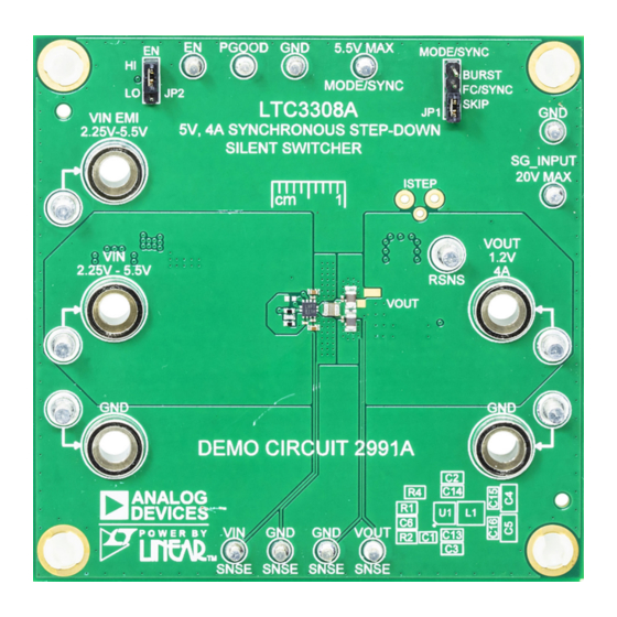
Demonstration circuit 2991A features the
5V, 4A synchronous step-down Silent Switcher
ating as a 2.0MHz, 3.3V to 1.2V 4A buck regulator. The
LTC3308A supports adjustable output voltages from 0.5V
to V
with operating frequencies from 1MHz up to 3MHz.
IN
The LTC3308A is a compact, ultralow emission, high
efficiency, and high speed synchronous monolithic step-
down switching regulator. A minimum on-time switching
of 22ns enables high V
IN
at high frequencies.
The DC2991A operating mode may be selected as BURST,
SKIP or Forced Continuous (FC) mode. Setting JP1 to
the FC/SYNC position will allow the LTC3308A to sync to
a clock frequency from 1MHz to 3MHz. The LTC3308A
operates in forced continuous mode when syncing to an
external clock. The DC2991A is set to a fixed 2MHz fre-
quency by connecting RT to V
The frequency can be easily changed by removing R9 and
setting an appropriate resistor in the R4 location to obtain
the desired frequency. Refer to the LTC3308A data sheet
for the proper RT value for a desired switching frequency.
PERFORMANCE SUMMARY
SYMBOL
PARAMETER
V
Input Voltage Range
IN
V
V
Voltage Range*
OUT
OUT
I
Output Current
OUT
f
Switching Frequency
SW
T
Top Switch Minimum On-Time
ON
Duty Cycle
Top Switch Duty Cycle
*With 1% resistors. Accuracy will improve to within 1% using 0.1% resistors.
5V Input to 1.2V Output at 4A Synchronous
Step‑Down Silent Switcher Demo Circuit
LTC
3308A
®
®
to low V
conversion ratios
OUT
through a 0Ω resistor, R9.
IN
Specifications are at T
CONDITIONS
V
IN
DEMO MANUAL DC2991A
The DC2991A also has an EMI filter to reduce conducted
oper-
EMI. This EMI filter can be included by applying the input
voltage at the V
the board is shown in the EMI Test Results section. The
red lines in the EMI performance graphs illustrate the
CISPR25 Class 5 peak limits for the conducted and radi-
ated emission tests.
The LTC3308A data sheet gives a complete description
of the device, operation and application information. The
data sheet must be read in conjunction with this demo
manual. The LTC3308A is assembled in a 2mm × 2mm
LQFN package with exposed pads for low thermal resis-
tance. The layout recommendations for low EMI operation
and maximum thermal performance are available in the
data sheet section: Low EMI PCB Layout.
The Efficiency vs Load graph shows the efficiency and
the power loss of the circuit with a 3.3V input in Burst
Mode operation.
Design files for this circuit board are
All registered trademarks and trademarks are the property of their respective owners.
= 25°C
A
Greater than V
OUT
LTC3308A
EMI terminal. The EMI performance of
IN
available.
MIN
TYP
2.25
1.183
1.2
1
22
MAX
UNITS
5.5
V
1.217
V
4
A
3
MHz
ns
100
%
Rev. 0
1
Advertisement
Table of Contents

Subscribe to Our Youtube Channel
Related Manuals for Analog Devices LTC3308A


Summary of Contents for Analog Devices LTC3308A
- Page 1 The DC2991A operating mode may be selected as BURST, manual. The LTC3308A is assembled in a 2mm × 2mm SKIP or Forced Continuous (FC) mode. Setting JP1 to LQFN package with exposed pads for low thermal resis- the FC/SYNC position will allow the LTC3308A to sync to tance.
-
Page 2: Circuit Schematic
Burst Mode Operation = 2.25V TO 5.5V 1µF 1µF 4.7µF 4.7µF EFFICIENCY 0201 0201 330nH 1.2V 10pF 140k 33µF LTC3308A 0.01 POWER LOSS 100k = 3.3V 10nF MODE/SYNC = 1.2V 0.001 AGND = 2 MHz PGND PGOOD Murata DFE201210S–R47M 0.0001... - Page 3 (WITH EMI FILTER INSTALLED) 3.3V INPUT TO 1.2V OUTPUT AT 3.2A, f = 2MHz 3.3V INPUT TO 1.2V OUTPUT AT 3.2A, f = 2MHz Load Transient Response Forced Continuous Mode LTC3308A Load Regulation 1.210 = 3.3V SG_INPUT 1.208 = 1.2V...
- Page 4 Demonstration circuit 2991A is easy to set up and use 9. Set the load current to 0.3A and repeat Step 8. Observe to evaluate the performance of the LTC3308A. Refer to that the switching waveform is now operating in pulse- Figure 1 for proper measurement equipment setup and...
-
Page 5: Quick Start Procedure
DEMO MANUAL DC2991A QUICK START PROCEDURE Figure 1. Test Setup for the DC2991A Demo Board Figure 2. Technique for Measuring Output Ripple Figure 3. Technique for Measuring Output Ripple and Step and Step Response with a Scope Probe Response with a Low Inductance Connector (Not Supplied) Rev. -
Page 6: Theory Of Operation
TON of 42ns inductor then increases until the top switch comparator in Equation 1. trips and turns off the top power switch. If the EN pin is low, the LTC3308A is in shutdown and in a low quiescent SWMAX •TON INMAX current state. - Page 7 THEORY OF OPERATION to the output capacitors as close to the inductor as pos- Accurately Measuring Output Ripple of the LTC3308A sible. Adding capacitors close to the load creating a π With the fast edge rates of the circuit, high frequency...
- Page 8 RES., 140k, 1%, 1/16W, 0402, AEC-Q200 VISHAY, CRCW0402140KFKED RES., 100k, 1%, 1/16W, 0402, AEC-Q200 VISHAY, CRCW0402100KFKvED IC, 5V, 4A SYNCHRONOUS STEP-DOWN Silent Switcher, LQFN ANALOG DEVICES, LTC3308AEV#PBF Additional Demo Board Circuit Components C7, C8 CAP ., 330μF, TANT. POSCAP , 6.3V, 20%, 7343, 25mΩ, TPE PANASONIC, 6TPE330ML CAP ., 0.1μF, X7R, 16V, 10%, 0402, AEC-Q200...
-
Page 9: Schematic Diagram
Devices for its use, nor for any infringements of patents or other rights of third parties that may result from its use. Specifications subject to change without notice. No license is granted by implication or otherwise under any patent or patent rights of Analog Devices. - Page 10 Board until you have read and agreed to the Agreement. Your use of the Evaluation Board shall signify your acceptance of the Agreement. This Agreement is made by and between you (“Customer”) and Analog Devices, Inc. (“ADI”), with its principal place of business at One Technology Way, Norwood, MA 02062, USA. Subject to the terms and conditions of the Agreement, ADI hereby grants to Customer a free, limited, personal, temporary, non-exclusive, non-sublicensable, non-transferable license to use the Evaluation Board FOR EVALUATION PURPOSES ONLY.
Need help?
Do you have a question about the LTC3308A and is the answer not in the manual?
Questions and answers