Table of Contents
Advertisement
Quick Links
Advertisement
Table of Contents

Subscribe to Our Youtube Channel
Related Manuals for Tews Technologies TPMC866-10R


Summary of Contents for Tews Technologies TPMC866-10R
- Page 1 The Embedded I/O Company TPMC866-10R/-11R 8 Channel Serial Interface Version 1.1 User Manual Issue 1.1.2 March 2021 TEWS TECHNOLOGIES GmbH Am Bahnhof 7 25469 Halstenbek, Germany Phone: +49 (0) 4101 4058 0 Fax: +49 (0) 4101 4058 19 e-mail: info@tews.com...
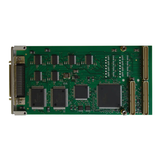
- Page 2 8 channel RS232 serial interface PMC with front TEWS TECHNOLOGIES GmbH is not liable for any I/O and P14 I/O, extended temperature range damage arising out of the application or use of the device described herein.
- Page 3 Corrected RxD signal names in pin assignment table 1.1.0 Document Update caused by new Hardware Version April 2013 1.1.1 General Revision August 2014 1.1.2 Discarded RS485 Reference in Block Diagram March 2021 TPMC866-10R/-11R User Manual Issue 1.1.2 Page 3 of 27...
-
Page 4: Table Of Contents
Front Panel I/O..........................24 9.1.1 Connector........................24 9.1.2 Front panel I/O Assignment TPMC866-10R / -11R............24 Back Panel I/O ..........................26 9.2.1 Mezzanine Card Connector P14 ..................26 9.2.2 Back panel I/O Assignment TPMC866-10R / -11R ............26 TPMC866-10R/-11R User Manual Issue 1.1.2 Page 4 of 27... - Page 5 TABLE 5-1 : LOCAL BUS LITTLE/BIG ENDIAN ..................18 TABLE 7-1 : BAUD RATE PROGRAMMING TABLE ................. 21 TABLE 9-1 : I/O CONNECTOR PIN ASSIGNMENT .................. 25 TABLE 9-2 : I/O CONNECTOR PIN ASSIGNMENT .................. 27 TPMC866-10R/-11R User Manual Issue 1.1.2 Page 5 of 27...
-
Page 6: Product Description
The receiver signal termination for each channel (120ohm between RxD+ and RxD-) is provided on board the TPMC866. Each channel of the TPMC866-10R/11R has a 64 byte transmit FIFO and a 64 byte receive FIFO to significantly reduce the overhead required to provide data to and get data from the transmitters and receivers. -
Page 7: Technical Specification
Number of Serial Channels Physical Interface TPMC866-10R: RS232, TPMC866-11R: RS422 I/O Signals TPMC866-10R: TxD, RxD, RTS, CTS, GND Additionally for Channel 1 and 2: DTR, DSR, DCD, RI TPMC866-11R: TxD+, TxD-, RxD+, RxD-, GND On Board Termination TPMC866-11R: 120 ohms between RxD+ and RxD- for each... -
Page 8: Local Space Addressing
Serial Channel 6 Register Set 0x38 to 0x3F Serial Channel 7 Register Set 0x40 FIFO Ready Register CH0-CH3 0x44 FIFO Ready Register CH4-CH7 0x48 Interrupt Status Register Table 3-2 : Local Register Space 1 TPMC866-10R/-11R User Manual Issue 1.1.2 Page 8 of 27... -
Page 9: Serial Channel Register Set
FIFO Control Register 0x03 Line Control Register (LCR) 0x04 Modem Control Register 0x05 Line Status Register 0x06 Modem Status Register 0x07 Scratchpad Register Scratchpad Register Table 3-4 : Channel Register Set 1 TPMC866-10R/-11R User Manual Issue 1.1.2 Page 9 of 27... -
Page 10: Channel Register Set 2
LCR set to 0xBF 0x05 Xon-2 Word LCR set to 0xBF 0x06 Xoff-1 Word LCR set to 0xBF 0x07 Xoff-2 Word LCR set to 0xBF Table 3-5 : Channel Register Set 2 TPMC866-10R/-11R User Manual Issue 1.1.2 Page 10 of 27... -
Page 11: Other Registers
1 = one or more empty locations exist in the TXRDY corresponding FIFO Channel 1 TXRDY Channel 0 Table 3-7 : FIFO Ready Register 1 (Channel 0-3) TPMC866-10R/-11R User Manual Issue 1.1.2 Page 11 of 27... -
Page 12: Fifo Ready 2 Register Channel 4-7
1 = one or more empty locations exist in the TXRDY corresponding FIFO Channel 5 TXRDY Channel 4 Table 3-8 : FIFO Ready Register 2 (Channel 4-7) TPMC866-10R/-11R User Manual Issue 1.1.2 Page 12 of 27... -
Page 13: Interrupt Status Register
Status Register can be used as an interrupt status polling register for the 8 serial channels. Interrupts of the 8 serial channels can be individually enabled / disabled by the ST16C654 UART registers. After reset all interrupts are disabled. TPMC866-10R/-11R User Manual Issue 1.1.2 Page 13 of 27... -
Page 14: Pci9030 Target Chip
VPD Nxt Cap. VPD Cap. ID Y[31:16] 0000 00 03 0x50 VPD Data 00000000 Table 4-1 : PCI9030 Header Device-ID: 0x9050 (PCI9050) Vendor-ID: 0x10B5 (PLX Technology) Subsystem-ID: 0x0362 (TPMC866) Subvendor-ID: 0x1498 (TEWS TECHNOLOGIES) TPMC866-10R/-11R User Manual Issue 1.1.2 Page 14 of 27... -
Page 15: Local Configuration Register (Lcr)
General Purpose I/O Control 0x0000_0246 0x70 Hidden1 Register for Power Management Data Select 0x0000_0000 0x74 Hidden 2 Register for Power Management Data Scale 0x0000_0000 Table 4-2 : PCI9030 Local Configuration Register TPMC866-10R/-11R User Manual Issue 1.1.2 Page 15 of 27... -
Page 16: Configuration Eeprom
0xFFFF 0xFFFF 0xFFFF 0xFFFF 0xFFFF 0xFFFF 0xFFFF 0xE0 0xFFFF 0xFFFF 0xFFFF 0xFFFF 0xFFFF 0xFFFF 0xFFFF 0xFFFF 0xF0 0xFFFF 0xFFFF 0xFFFF 0xFFFF 0xFFFF 0xFFFF 0xFFFF 0xFFFF Table 4-3 : Configuration EEPROM TPMC866-xx TPMC866-10R/-11R User Manual Issue 1.1.2 Page 16 of 27... -
Page 17: Local Software Reset
PCI9030 remains in this reset condition until the PCI Host clears this bit. The contents of the PCI9030 PCI and Local Configuration Registers are not reset. The PCI9030 PCI Interface is not reset. TPMC866-10R/-11R User Manual Issue 1.1.2 Page 17 of 27... -
Page 18: Configuration Hints
Byte 0 D[15..8] Byte 1 D[7..0] 8 Bit upper lane 8 Bit Byte 0 D[31..24] Byte 0 D[7..0] 8 Bit lower lane Byte 0 D[7..0] Table 5-1 : Local Bus Little/Big Endian TPMC866-10R/-11R User Manual Issue 1.1.2 Page 18 of 27... - Page 19 0x34 Local Address Space 0 Bus Region Description Register EROMBRD 0x38 Expansion ROM Bus Region Description Register You could also use the PCI - Base Address 1 I/O Mapped Configuration Registers. TPMC866-10R/-11R User Manual Issue 1.1.2 Page 19 of 27...
-
Page 20: Functional Description
6 Functional Description For a detailed description of the UART functions please refer to the 16C654 UART data sheet (Exar). TPMC866-10R/-11R User Manual Issue 1.1.2 Page 20 of 27... -
Page 21: Programming Hints
These steps should be used to modify the DLM, DLL registers : Write 0x80 to LCR register (enable access to DLM, DLL registers) Modify DLM, DLL registers Write normal operation byte value to LCR register TPMC866-10R/-11R User Manual Issue 1.1.2 Page 21 of 27... - Page 22 Write 0xBF to LCR register (enable access to EFR register) Set EFR register bit 4 to '0' (Latch MCR bit setting) Write normal operation byte value to LCR register TPMC866-10R/-11R User Manual Issue 1.1.2 Page 22 of 27...
-
Page 23: Installation Hints
The TPMC866-11R (RS422) provides on board 120ohms termination resistors. Do not apply additional external 120ohms termination resistors here. Please note that on the TPMC866-10R and TPMC866-11R, the P14 back I/O connector is always populated and connected to on board logic. Do not use these modules on carrier boards where P14/J14 is reserved for other system signals but PMC I/O. -
Page 24: Pin Assignment - I/O Connector
Pin 1 Pin 25 Pin 50 Pin 26 Figure 9-1 : Front Panel I/O Connector Numbering 9.1.2 Front panel I/O Assignment TPMC866-10R / -11R The subsequent figure shows the complete assembled pin front panel I/O connector. Pin Number TPMC866-10R TPMC866-11R... -
Page 25: Table 9-1 : I/O Connector Pin Assignment
Ring Indicator CH0 DSR0 Data Set Ready CH0 Data Carrier Detect CH1 DTR1 Data Terminal Ready CH1 Ring Indicator CH1 DSR1 Data Set Ready CH1 Table 9-1 : I/O Connector Pin Assignment TPMC866-10R/-11R User Manual Issue 1.1.2 Page 25 of 27... -
Page 26: Back Panel I/O
Back Panel I/O 9.2.1 Mezzanine Card Connector P14 MOLEX 71436-216 or compatible 9.2.2 Back panel I/O Assignment TPMC866-10R / -11R The subsequent figure shows the complete assembled pin back panel I/O connector. Pin Number TPMC866-10R TPMC866-11R Comment RS232 Interface RS422 Interface... -
Page 27: Table 9-2 : I/O Connector Pin Assignment
The TPMC866-11R (RS422) provides on board 120ohms termination resistors. Do not apply additional external 120ohms termination resistors here. Please note that on the TPMC866-10R and TPMC866-11R, the P14 back I/O connector is always populated and connected to on board logic. Do not use these modules on carrier boards where P14/J14 is reserved for other system signals but PMC I/O.
Need help?
Do you have a question about the TPMC866-10R and is the answer not in the manual?
Questions and answers