Sign In
Upload
Download
Table of Contents
Contents
Add to my manuals
Delete from my manuals
Share
URL of this page:
HTML Link:
Bookmark this page
Add
Manual will be automatically added to "My Manuals"
Print this page
×
Bookmark added
×
Added to my manuals
Manuals
Brands
LG Manuals
DVD Drive
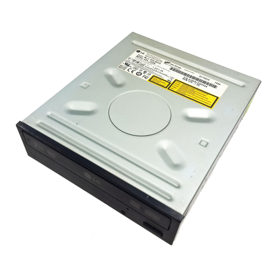
GSA-H20A
Service manual
LG GSA-H20A Service Manual
Super-multi dvd rewriter
Hide thumbs
1
Table Of Contents
2
3
4
5
6
7
8
9
10
11
12
13
14
15
16
17
18
19
20
21
22
23
24
25
26
27
28
29
30
31
32
33
34
35
36
37
38
39
40
41
42
43
44
45
46
47
48
49
50
51
52
53
54
55
56
57
58
59
60
61
62
63
64
65
66
67
68
69
70
71
72
73
74
75
76
77
78
79
80
81
82
83
84
85
86
page
of
86
Go
/
86
Contents
Table of Contents
Troubleshooting
Bookmarks
Table of Contents
Table of Contents
Introduction
Features
Specifications
Location of Customer Controls
Disassembly
CABINET and CIRCUIT BOARD DISASSEMBLY
Mechanism Assy Disassembly
Mechanical Replacement Parts List
Exploded View
Glossary
The Differences of CD-R/CD-Rw Discs and General CD-Rom
Recording Layer
Disc Specification
Disc Materials
Reading Process of Optical Disc
Writing Process of CD-R Disc
Writing Process of CD-RW Disc
Organization of the PCA, PMA and Lead-In Area
Function of PCA and PMA Area
OPC and ROPC
Writing Process of DISC
The Differences of DVD-R/Rw, DVD+R/Rw Discs and DVD-Rom
Recording Layer
Disc Specification
Disc Materials
Writing Pulse Waveform of DVD+R
Writing Pulse Waveform DVD+RW
Organization of Inner Drive Area, Outer Drive Area, Lead-In Zone and Lead-Out Zone
Lightscribe MEDIA
Hardware Block Diagram of Lightscribe Label Printing
MD Assy for Lightscribe
Optical Encoder Assy
DVD & CD Data Processing
Data Processing Flow
Copy Protection and Regional Code Management Block
About Prevention the DVD-Rom from to be Copy
About the DVD-ROM Regional Code
Internal Structure of the Pick
Block Diagram of the Pick-Up
Pick up Pin Assignment
Signal Detection of the P/U
Description of Circuit
ALPC Circuit
Focus/Tracking/Sled Servo Circuit
Spindle Circuit
Major IC Internal Block Diagram and Pin Description
Troubleshooting Guide
How to Use Test Tool
Dragon
Camus
Block Diagram
Advertisement
Quick Links
1
Features
2
Specifications
3
Writing Process of CD-R Disc
Download this manual
Super-Multi DVD Rewriter
SERVICE MANUAL
MODEL: GSA-H20A/
P/NO : 3828HS1049E
MODEL : GSA-H20A/GSA-H20N/GSA-H20L
GSA-H20N/
GSA-H20L
may, 2006
Printed in Korea
Table of
Contents
Previous
Page
Next
Page
1
2
3
4
5
Advertisement
Table of Contents
Need help?
Do you have a question about the GSA-H20A and is the answer not in the manual?
Ask a question
Questions and answers
Related Manuals for LG GSA-H20A
DVD Drive LG GSA-H20L Owner's Manual
Super multi dvd drive (18 pages)
DVD Drive LG GSA-H21N Specifications
Combo optical drive (2 pages)
DVD Drive LG GSA-H22L Specifications
18x super multi dvd rewriter (1 page)
DVD Drive LG GSA-H20N Service Manual
Super-multi dvd rewriter (86 pages)
DVD Drive LG GH22NS40 Owner's Manual
Gh22 series super multi dvd rewriter (13 pages)
DVD Drive LG GSA-H58N Owner's Manual
Super multi dvd rewriter (14 pages)
DVD Drive LG GSA-H44N Owner's Manual
Super multi dvd rewriter (15 pages)
DVD Drive LG GSA-H10A Owner's Manual
Super multi dvd drive (14 pages)
DVD Drive LG GSA-H50N Owner's Manual
(14 pages)
DVD Drive LG GSA-H42N Owner's Manual
Super multi dvd rewriter (15 pages)
DVD Drive LG GSA-H12N Owner's Manual
Super multi dvd rewriter (15 pages)
DVD Drive LG GSA-4167B Service Manual
Super multi dvd drive (86 pages)
DVD Drive LG GSA-2164D User Manual
External super multi dvd rewriter (15 pages)
DVD Drive LG GSA-5163D Service Manual
External super multi dvd rewriter (76 pages)
DVD Drive LG GSA-5163D Owner's Manual
External super multi dvd rewriter (15 pages)
DVD Drive LG GCC-4242N Service Manual
Slim cd-rw/dvd-rom drive (69 pages)
This manual is also suitable for:
Gsa-h20n
Gsa-h20l
Gsa-h20v
Gsa-h21n
Gsa-h21l
Gsa-h21v
...
Show all
Gsa-h21a
Table of Contents
Save PDF
Print
Rename the bookmark
Delete bookmark?
Delete from my manuals?
Login
Sign In
OR
Sign in with Facebook
Sign in with Google
Upload manual
Upload from disk
Upload from URL


Need help?
Do you have a question about the GSA-H20A and is the answer not in the manual?
Questions and answers