
Related Manuals for National Instruments GPIB-1014


Summary of Contents for National Instruments GPIB-1014
- Page 1 GPIB-1014 User Manual March 1997 Edition Part Number 3 70945A-01 © Copyright 1985, 1997 National Instruments Corporation. All Rights Reserved.
- Page 2 National Instruments Corporate Headquarters 6504 Bridge Point Parkway Austin, TX 78730-5039 (512) 794-0100 Technical support phone: (512) 795-8248 Technical support fax: (512) 794-5678 Branch Offices: Australia 03 9879 5166, Austria 0662 45 79 90 0, Belgium 02 757 00 20, Canada (Ontario) 905 785 0085, Canada (Québec) 514 694 8521, Denmark 45 76 26 00, Finland 90 527 2321, France 1 48 14 24 24,...
- Page 3 Limited Warranty The GPIB-1014 is warranted against defects in materials and workmanship for a period of two years from the date of shipment, as evidenced by receipts or other documentation. National Instruments will, at its option, repair or replace equipment that proves to be defective during the warranty period. This warranty includes parts and labor.
- Page 4 Any use or application of National Instruments products for or involving medical or clinical treatment must be performed by properly trained and qualified medical personnel, and all traditional medical safeguards, equipment, and procedures that are appropriate in the particular situation to prevent serious injury or death should always continue to be used when National Instruments products are being used.
- Page 5 Notice to user: Changes or modifications not expressly approved by National Instruments could void the user’s authority to operate the equipment under the FCC Rules. If necessary, consult National Instruments or an experienced radio/television technician for additional suggestions.
-
Page 6: Table Of Contents
Data Transfer Bus (DTB) Requester ..............2-7 VMEbus Modules Not Provided ............2-7 Diagnostic Aids ....................2-7 Data Transfer Features ....................2-7 Programmed I/O Transfers ................2-8 GPIB-1014 Functional Description ................2-8 Chapter 3 Configuration and Installation ..................3-1 Configuration......................... 3-1 Access Mode ..................... - Page 7 Chapter 5 Programming Considerations ..................5-1 Initialization........................5-1 The GPIB-1014 as GPIB Controller ................5-3 Becoming Controller-In-Charge (CIC) and Active Controller ......5-3 Sending Remote Multiline Messages (Commands) .......... 5-4 Going from Active to Standby Controller ............5-4 GPIB-1014 User Manual viii ©...
- Page 8 Going from Standby to Active Controller ............5-4 Going from Active to Idle Controller ..............5-5 The GPIB-1014 as GPIB Talker and Listener............... 5-6 Programmed Implementation of Talker and Listener ........5-6 Addressed Implementation of the Talker and Listener ........5-6 Address Mode 1..................
- Page 9 DMA Stand-Alone Testing ................6-24 GPIB Interface Testing..................6-24 Chapter 7 Diagnostic and Troubleshooting Test Procedures ..........7-1 Interpreting Test Procedures ..................7-1 GPIB-1014 Hardware Installation Tests ............... 7-2 Appendix A Hardware Specifications ....................A-1 Appendix B Parts List and Schematic Diagrams ................
- Page 10 Parts Locator Diagram ..................3-2 Figure 3-2. Access Mode After RESET ................3-3 Figure 3-3. Configuration for GPIB-1014 Base Address 2000 (hex) ......... 3-4 Figure 3-4. Default Settings of AM Code Jumpers W3, W4, and W5 ....... 3-5 Figure 4-1.
- Page 11 Programming Values for Default Settings of W3, W4, and W5 ....... 3-6 Table 3-2. Setting the Address Modifier Code Bits (AM5-AM0)........3-6 Table 3-3. GPIB-1014 Pin Assignment on VMEbus Connector P1 ........3-8 Table 3-4. GPIB-1014 Pin Assignment on VMEbus Connector P2 ........3-9 Table 4-1.
-
Page 12: About This Manual
Chapter 5, Programming Considerations, explains the initialization process, sending/receiving messages, and the serial/parallel poll process. • Chapter 6, Theory of Operation, contains a functional overview of the GPIB-1014 board and explains the operation of each functional block making up the GPIB-1014. •... -
Page 13: Conventions Used In This Manual
• Appendix G, Customer Communication, contains forms for you to complete to facilitate communication with National Instruments concerning our products. • The Glossary contains an alphabetical list and description of terms used in this manual, including abbreviations, acronyms, metric prefixes, and symbols. -
Page 14: Customer Communication
Hitachi Microcomputer System HD68450 DMAC (Direct Memory Access Controller) Customer Communication National Instruments wants to receive your comments on our products and manuals. We are interested in the applications you develop with our products, and we want to help if you have problems with them. -
Page 15: Chapter 1 Introduction
Chapter 1 Introduction This chapter describes the GPIB-1014, lists the contents and oiptional equipment for your GPIB-1014 kit, and explains how to unpack the GPIB-1014 kit. The GPIB-1014 is a high-performance IEEE 488 interface for the VMEbus. This interface permits IEEE 488 compatible engineering, scientific, or medical instruments to be controlled from a VMEbus-based computer. -
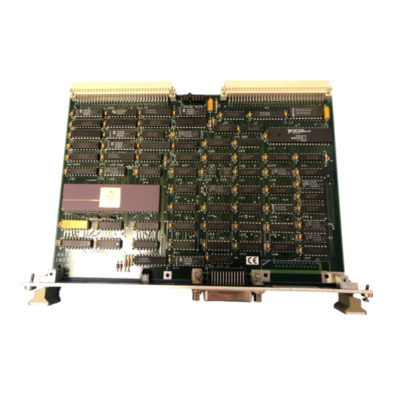
Page 16: Figure 1-1. Gpib-1014 Interface Board
Introduction Chapter 1 Figure 1-1 shows the GPIB-1014 interface board. Art not available in PDF version of document. Figure 1-1. GPIB-1014 Interface Board GPIB-1014 User Manual © National Instruments Corporation... -
Page 17: What Your Kit Should Contain
Chapter 1 Introduction The GPIB-1014 interface kit includes hardware and programming examples to implement the GPIB functions. Optional cables are supplied for interconnection with other devices on the GPIB. What Your Kit Should Contain Your GPIB-1014 kit should contain the following components:... -
Page 18: Unpacking
Do not remove the board from its plastic bag at this point. 2. Your GPIB-1014 board is shipped packaged in an antistatic plastic bag to prevent electrostatic damage to the board. Several components on the board can be damaged by electrostatic discharge. - Page 19 Electrical Characteristics All integrated circuit drivers and receivers used on the GPIB-1014 meet the requirements of the VMEbus specification and the IEEE 1014 standard. Table 2-1 contains a list of the VMEbus signals used by the GPIB-1014 and the electrical loading presented by the circuitry on the interface board (in terms of device types and their part numbers).
-
Page 20: General Description
VMEbus Slave-Addressing The GPIB-1014 occupies 512 bytes (256 words) in the A16 (short) I/O space. As a VMEbus slave, it only responds when the address modifier (AM) lines specify a short supervisory access (AM code = 2D) or a short nonprivileged access (AM code = 29). The board responds to short 16-bit addresses. -
Page 21: Vmebus Slave-Data
Table 2-2. The DMA registers internal to the 68450 are shown in Table 2-3. The two Configuration Registers of the GPIB-1014 are shown in Table 2-4. Table 2-2. µPD7210 Internal GPIB Interface Registers... -
Page 22: Table 2-3. 68450 Internal Dma Registers
Base Transfer Counter (BTCR2) 16 bits Base Address Register (BAR2) 32 bits Base Function Code (BFCR2) 8 bits Channel Status (CSR2) 8 bits Channel Error (CER2) 8 bits Device Control (DCR2) 8 bits (continues) GPIB-1014 User Manual © National Instruments Corporation... -
Page 23: Vmebus Master-Direct Memory Access
8 bits VMEbus Master-Direct Memory Access The GPIB-1014 can function as a VMEbus master, performing data transfers to and from VMEbus memory. In most applications, the 68450 controls the data transfer to and from the GPIB during DMA, and can transfer the 8-bit data on data lines D07 through D00 or D15 through D08, allowing the packing of data in VMEbus memory. -
Page 24: Interrupter
I/O area. In VMEbus terminology, the GPIB-1014 has A24 / D08(EO) & D16 master capability. The board does not use Unaligned Transfer (UAT), Block Transfer (BLT), or Read Modify Write (RMW) cycles. The chaining feature of the 68450 allows data blocks of unlimited size to be transferred. -
Page 25: Data Transfer Bus (Dtb) Requester
Chapter 7, Diagnostic and Troubleshooting Test Procedures, for details. Data Transfer Features The GPIB-1014 can be used to transfer data to and from the GPIB using Direct Memory Access (DMA) and programmed I/O. The overall throughput is dependent upon the following parameters: •... -
Page 26: Programmed I/O Transfers
Programmed I/O Transfers The GPIB-1014 is able to transfer data to and from the GPIB using programmed I/O. Transfer rates using programmed I/O depend on many factors including how fast the program code executes, how fast the microprocessor services interrupts, and the operating system overhead. -
Page 27: Figure 2-1. Gpib-1014 With A Vmebus Computer
NRFD (Not Ready for Data) NDAC (Not Data Accepted) Management Lines 5 Lines IFC (Interface Clear) ATN (Attention) SRQ (Service Request) REN (Remote Enable) EOI (End or Identify) Figure 2-1. GPIB-1014 with a VMEbus Computer © National Instruments Corporation GPIB-1014 User Manual... -
Page 28: Figure 2-2. Gpib-1014 In A Multiprocessor Application
Up to 300 Meters (RS-422) Computer Center GPIB-100 Bus Extender Production & Testing PDP 11/44 with GPIB11-2 S-100 Computer IEEE 488 Interface GPIB-696P IEEE 488 Interface Figure 2-2. GPIB-1014 in a Multiprocessor Application GPIB-1014 User Manual 2-10 © National Instruments Corporation... -
Page 29: Figure 2-3. Gpib-1014 Block Diagram
Chapter 2 General Description Figure 2-3 is a block diagram of the GPIB-1014. GPIB Configuration Registers µPD7210 68450 DMAC Interrupter Data Transfer Bus Priority Interrupt DTB Arbitration Utility Figure 2-3. GPIB-1014 Block Diagram © National Instruments Corporation 2-11 GPIB-1014 User Manual... - Page 30 Implements many of the GPIB interface functions, either independently or with assistance of or interpretation by the controlling program. Together with special transceivers, the TLC forms the GPIB interface side of the GPIB-1014. GPIB-1014 User Manual 2-12 © National Instruments Corporation...
-
Page 31: Table 2-5. Gpib-1014 Ieee 488 Interface Capabilities
Chapter 2 General Description Table 2-5 lists the capabilities of the GPIB-1014 in terms of the IEEE 488 standard codes. Table 2-5. GPIB-1014 IEEE 488 Interface Capabilities Capability Code Description Complete Source Handshake capability Complete Acceptor Handshake capability DAC and RFD... - Page 32 The GPIB-1014 has complete Source and Acceptor Handshake capability. • The GPIB-1014 can operate as a basic Talker or Extended Talker and can respond to a Serial Poll. It can be placed in a Talk Only mode and is unaddressed to talk when it receives its listen address.
-
Page 33: Table 2-6. Gpib-1014 Ieee 1014 Interrupter Compliance Levels
• Pass control • Conduct a Parallel Poll • Take control synchronously or asynchronously Table 2-6 contains the GPIB-1014 IEEE 1014 compliance levels. Table 2-6. GPIB-1014 IEEE 1014 Interrupter Compliance Levels Compliance Notation Description Bus Slave Compliance Levels D8(O) 8-bit data path to TLC and two Configuration Registers D16 &... -
Page 34: Configuration And Installation
Chapter 3 Configuration and Installation This chapter describes the steps needed to configure and install the GPIB-1014 hardware. Configuration Before installing the GPIB-1014 in the VMEbus backplane, the following options must be configured with hardware jumpers that are located on the GPIB-1014 interface board: •... -
Page 35: Figure 3-1. Parts Locator Diagram
Configuration and Installation Chapter 3 Figure 3-1 shows the locations of the GPIB-1014 configuration jumpers and switches. Figure 3-1. Parts Locator Diagram GPIB-1014 User Manual © National Instruments Corporation... -
Page 36: Access Mode
Figure 3-2. Access Mode After RESET Base Address The GPIB-1014 occupies a total of 512 bytes of 16-bit I/O space. The base address is selected with either hardware jumper block W1 on the interface board or compare address lines located on the P2 connector. -
Page 37: Set Base Address Using Jumper Block W1
0 to select a logical zero. Figure 3-3 shows the configuration for a base address 2000 (hex), which is the default address configured at the factory. BASE ADD Figure 3-3. Configuration for GPIB-1014 Base Address 2000 (hex) (Default Setting) Set Base Address Using Compare Address Lines Another method of setting the base address is to use the compare address lines located on the P2 connector. -
Page 38: Dma Address Modifier Code Output
Figure 3-4. Default Settings of AM Code Jumpers W3, W4, and W5 Rev. D and earlier versions of the GPIB-1014 do not have jumpers W3, W4, and W5. If all of the jumpers on later versions of the board remain in their factory default settings, the address modifier codes generated are equivalent to those generated by the earlier versions. -
Page 39: Table 3-1. Programming Values For Default Settings Of W3, W4, And W5
0 or 1 None AM(3) Jumper W4 0 or 1 AM(2) Bit M2 in FCR 0 or 1 None AM(1) Bit M0 in FCR 0 or 1 None AM(0) Jumper W5 AM(1) or AM(1)' AM(1)' GPIB-1014 User Manual © National Instruments Corporation... -
Page 40: Other Configuration Parameters
Tables 3-3 and 3-4 to those signals used by the VMEbus system in which the GPIB-1014 will be installed. This is to ensure that the two are compatible (that is, the GPIB-1014 has all the necessary signals needed by the system and vice versa). -
Page 41: Table 3-3. Gpib-1014 Pin Assignment On Vmebus Connector P1
Configuration and Installation Chapter 3 Table 3-3. GPIB-1014 Pin Assignment on VMEbus Connector P1 Pin No. Signal Used Signal Not Used Pin No. Signal Used Signal Not Used IACK* IACKIN* IACKOUT* SYSCLK DS1* DS0* WRITE* -12V DTACK* BBSY* BCLR* ACFAIL*... -
Page 42: Table 3-4. Gpib-1014 Pin Assignment On Vmebus Connector P2
Compare Address lines. Can be used to set base address of GPIB-1014. GPIB signals used for GPIB I/O via P2. Reserved pin. Defined by the VMEbus specification. For models GPIB-1014-1S and GPIB-1014-1S-EH. These signals are not connected to the P2 connector. © National Instruments Corporation GPIB-1014 User Manual... -
Page 43: Cabling
Model GPIB-1014-1 is installed in the system, they cannot be placed side by side due to the width of the GPIB cable connector housing (another board must be placed between any two GPIB-1014-1 interface boards). -
Page 44: Table 4-1. Gpib-1014 Register Map
DMA registers. Register Map The register map for the GPIB-1014 is shown in Table 4-1. This table gives the register name, the register address, the register size in bits, and the register type (read only, write only, or read and write). -
Page 45: Register Bit Descriptions
VMEbus computers support three transfer sizes for read and write operations: 8-, 16-, or 32-bit. Table 4-1 shows the size of each GPIB-1014 register. For example, reading the Memory Transfer Counter Register requires a 16-bit read operation at the indicated address, whereas writing to the End Of String Register requires an 8-bit write operation at the indicated address. -
Page 46: Register Description Format
Chapter 4 Register Bit Descriptions Register Description Format The remainder of this chapter discusses each of the GPIB-1014 registers in the order shown in Table 4-1. Each register group is introduced, followed by a detailed bit description of each register. -
Page 47: Interface Registers
NEC µPD7210 Talker/Listener/Controller (TLC) integrated circuit. Each of the 21 interface registers is addressed relative to the GPIB-1014 VMEbus base address. Figures 4-1 and 4-2 show the register and bit mnemonics of each TLC internal register, its read/write accessibility, and its relative address. -
Page 48: Figure 4-1. Interface Registers
AD5-0 AD4-0 AD3-0 AD2-0 AD1-0 ADR0 +11D ADR1 AD5-1 AD4-1 AD3-1 AD2-1 AD1-1 +11F EOS7 EOS6 EOS5 EOS4 EOS3 EOS2 EOS1 EOS0 EOSR Note: X indicates bit is not used. Figure 4-1. Interface Registers © National Instruments Corporation GPIB-1014 User Manual... -
Page 49: Figure 4-2. Writing To The Hidden Registers
CLK1 CLK0 PPR is loaded with: AUXRA is loaded with: XEOS REOS HLDE HLDA AUXRB is loaded with: SPEOI ENABLE AUXRE is loaded with: DHDC DHDT Figure 4-2. Writing to the Hidden Registers GPIB-1014 User Manual © National Instruments Corporation... -
Page 50: Data In Register (Dir)
DI0 is the least significant bit of the data byte and corresponds to GPIB DI01. DI7 is the most significant bit of the data byte and corresponds to GPIB DI08. Mnemonic Description 7-0r DI[7-0] Data In Bits 7 through 0 © National Instruments Corporation GPIB-1014 User Manual... -
Page 51: Command/Data Out Register (Cdor)
DIR. When a byte is written to the CDOR, the TLC GPIB Source Handshake (SH) function is initiated and the byte is transferred to the GPIB. Mnemonic Description 7-0w CDO[7-0] Command/Data Out Bits 7 through 0 GPIB-1014 User Manual © National Instruments Corporation... -
Page 52: Interrupt Status Register 1 (Isr1)
+ (read ISR1) Notes UCG: GPIB Universal Command Group message ACG: GPIB Addressed Command Group message TADS: GPIB Talker Addressed State LADS: GPIB Listener Addressed State defined: GPIB command automatically recognized and executed by TLC © National Instruments Corporation GPIB-1014 User Manual... - Page 53 APT is cleared by: pon + (read ISR1) Notes ADM1: Address Mode Register Bit 1, ADMR[1]w ADM0: Address Mode Register Bit 0, ADMR[0]w TPAS: GPIB Talker Primary Addressed State LPAS: GPIB Listener Primary Addressed State GPIB-1014 User Manual 4-10 © National Instruments Corporation...
- Page 54 END RX is set by: LACS & (EOI + EOS & REOS) & ACDS END RX is cleared by: pon + (read ISR1) Notes LACS: GPIB Listener Active State EOI: GPIB End Of Identify Signal © National Instruments Corporation 4-11 GPIB-1014 User Manual...
- Page 55 ERR is cleared by: pon + (read ISR1) Notes TACS: GPIB Talker Active State SDYS: GPIB Source Delay State DAC: GPIB Data Accepted message RFD: GPIB Ready For Data message SIDS: GPIB Source Idle State GPIB-1014 User Manual 4-12 © National Instruments Corporation...
- Page 56 Data In Interrupt Enable Bit Bit DI is set by: LACS & ACDS & continuous mode DI is cleared by: pon + (read ISR1) + (Finish Handshake) & (Holdoff mode) + (read DIR) © National Instruments Corporation 4-13 GPIB-1014 User Manual...
- Page 57 DI IE must be clear so that an interrupt request does not occur. Instead, the DMAI bit in the Interrupt Mask Register 2 (IMR1[4]]w) must be set to enable a DMA cycle request when DI is asserted. GPIB-1014 User Manual 4-14 © National Instruments Corporation...
-
Page 58: Interrupt Status Register 2 (Isr2)
Enable Interrupt on Command Pass Through Bit APT: Address Pass Through Bit APT IE: Enable Interrupt on Address Pass Through Bit DET: Device Execute Trigger Bit DET IE: Enable Interrupt on Device Execute Trigger Bit ERR: Error Bit GPIB-1014 User Manual 4-14 © National Instruments Corporation... - Page 59 Mnemonic Description ERR IE: Enable Interrupt on Error Bit END RX: End Received Bit END IE: Enable Interrupt on End Received Bit DEC: Device Clear Bit DEC IE: Enable Interrupt on Device Clear Bit Data Out Bit DO IE: Enable Interrupt on Data Out Bit Data In Bit DI IE: Enable Interrupt on Data In Bit...
- Page 60 ISR2: Bit is cleared immediately after it is read CO = 1 indicates that the CDOR is empty and that another command can be written to it for transmission over the GPIB without overwriting a previous command. GPIB-1014 User Manual 4-16 © National Instruments Corporation...
- Page 61 Mnemonic Description LOKC Lockout Change Bit LOKC IE Lockout Change Interrupt Enable Bit LOKC is set by: any change in LOK LOKC is cleared by: pon + (read ISR2) Notes LOK: ISR2[5]r pon: Power On Reset read ISR2: Bit is cleared immediately after it is read LOKC is set when there is a change in the LOK bit, ISR2[5]r, (REMS +RELS).
- Page 62 ISR2: Bit is cleared immediately after it is read ADSR: Address Status Register ADMR: Address Mode Register ADSC is set when there is a change in one of the four bits–TA, LA, CIC, or MJMN–of the Address Status Register (ADSR). GPIB-1014 User Manual 4-18 © National Instruments Corporation...
-
Page 63: Serial Poll Status Register (Spsr)
Serial Poll Status Register (SPSR) VMEbus Address: Base Address + 117 (hex) Attributes: Read Only, Internal to TLC Serial Poll Mode Register (SPMR) VMEbus Address: Base Address + 117 (hex) Attributes: Write Only, Internal to TLC PEND Mnemonic Description Serial Poll Status Bit 8 5-0r, S[6-1] Serial Poll Status Bits 6 through 1... -
Page 64: Address Status Register (Adsr)
Register in this chapter), LPAS=1 indicates that the secondary address being received on the next GPIB command represents the TLC extended (secondary) GPIB listen address. LPAS is cleared by pon, by LMR (CR0[2]w), or by issuing the Chip Reset auxiliary command. GPIB-1014 User Manual 4-20 © National Instruments Corporation... - Page 65 Mnemonic Description TPAS Talker Primary Addressed State Bit TPAS is used when the TLC is configured for extended GPIB addressing, and, when set, indicates that the TLC has received its primary GPIB talk address. In extended mode addressing (mode 3 addressing), TPAS=1 indicates that the secondary address being received as the next GPIB command message can represent the TLC extended (secondary) GPIB talk address.
-
Page 66: Address Mode Register (Admr)
For proper operation, set both TRM1 and TRM0 to 1. These are set to configure the µPD7210 to match the transceivers chosen for hardware implementation of the GPIB interface. 3-2w Reserved Bits Write zeros to these bits. GPIB-1014 User Manual 4-22 © National Instruments Corporation... - Page 67 Mnemonic Description 1-0w ADM[1-0] Address Mode Bits 1 through 0 These bits state the addressing mode currently in effect–that is, the manner in which the information in ADR0 and ADR1 is interpreted (see Address Register 0 and Address Register 1 later in this chapter). If both bits are zero, then the TLC does not respond to GPIB address commands.
- Page 68 ADM0 and ADM1 must be cleared when either of the two programmable bits ton or lon is set. For more information on the different addressing modes supported by the GPIB-1014, refer to the Addressed Implementation of Talker and Listener section in Chapter 5.
-
Page 69: Command Pass Through Register (Cptr)
Command Pass Through Register (CPTR) VMEbus Address: Base Address + 11B (hex) Attributes: Read Only, Internal to TLC CPT7 CPT6 CPT5 CPT4 CPT3 CPT2 CPT1 CPT0 Mnemonic Description 7-0r CPT[7-0] Command Pass Through Bits 7 through 0 These bits are used to transfer undefined multiline GPIB command messages from the GPIB DIO lines to the computer. - Page 70 The CPTR is read during a TLC-initiated Parallel Poll operation to retrieve the Parallel Poll response. The PPR message is latched into the CPTR when CPPS is set, until CIDS is set, or until a command byte is sent over the GPIB. GPIB-1014 User Manual 4-26 © National Instruments Corporation...
-
Page 71: Auxiliary Mode Register (Auxmr)
Auxiliary Mode Register (AUXMR) VMEbus Address: Base Address + 11B (hex) Attributes: Write Only, Internal to TLC Permits Access to Hidden Registers CNT2 CNT1 CNT0 COM4 COM3 COM2 COM1 COM0 The Auxiliary Mode Register (AUXMR) is used to issue auxiliary commands. It is also used to program the five hidden registers: •... -
Page 72: Table 4-4. Auxiliary Command Summary
Set REN 1 0 1 1 1 Clear REN 1 0 1 0 0 Disable System Control * CNT[2-0] set to 000 binary ** Represents all eight bits of the Auxiliary Mode Register GPIB-1014 User Manual 4-28 © National Instruments Corporation... -
Page 73: Table 4-5. Auxiliary Commands: Detail Description
Table 4-5 shows the functions that are executed when the AUXMR Control Code (CNT2 through CNT0) is loaded with 000 (binary) and the Command Code (COM4 through COM0) is loaded. Table 4-5. Auxiliary Commands: Detail Description Command Code (COM4-COM0) 4 3 2 1 0 Description 0 0 0 0 0 Immediate Execute Pon... - Page 74 Holdoff on RFD or DAC. 0 0 1 0 0 Trigger Note: Trigger cannot be used with the GPIB-1014. The Trigger command generates a high pulse on the TRIG pin (T/R3 pin when TRM1=0) of the TLC. The Trigger command performs the same function as if the DET (Device Trigger) bit (ISR1[5]r) were set.
- Page 75 Table 4-5. Auxiliary Commands: Detail Description (continued) Command Code (COM4-COM0) 4 3 2 1 0 Description 0 0 0 0 1 Clear Parallel Poll Flag 0 1 0 0 1 Set Parallel Poll Flag These commands set the Parallel Poll Flag to the value of COM3. The value of the Parallel Poll Flag is used as the local message ist when bit four of Auxiliary Register B is zero.
- Page 76 (rsc) and set Interface Clear (IFC) to the value of COM3. These commands should only be issued if the System Controller (SC) bit in CFG2 is set; that is, the GPIB-1014 is SC. In order to meet the IEEE 488 requirements, you must not issue the Clear IFC command until IFC has been held true for at least 100 µsec.
-
Page 77: Hidden Registers
Chip Reset auxiliary command, by a Power On Reset, or by LMR (CR0[2]w). Figure 4-2 earlier in this chapter shows the five hidden registers and illustrates how they are loaded with data from the AUXMR. © National Instruments Corporation 4-33 GPIB-1014 User Manual... -
Page 78: Internal Counter Register (Icr)
AUXRB bit TRI. For proper operation, ICR should be set to eight because the TLC is clocked at 8 MHz. GPIB-1014 User Manual 4-34 © National Instruments Corporation... -
Page 79: Parallel Poll Register (Ppr)
PPE message, and the I/O write operation (to the PPR) is the same as the receipt of the PPE message from the GPIB Controller. When U=1, S and P[3-1] do not carry any meaning, but they must be cleared. © National Instruments Corporation 4-35 GPIB-1014 User Manual... -
Page 80: Table 4-6. Examples For Configuring The Ppr
PPR bits 3 through 1, designated P[3-1], contain an encoded version of the Parallel Poll response. P[3-1] indicate which of the eight DIO lines is asserted during a Parallel Poll (equal to N-1). The GPIB-1014 normally drives the GPIB DIO lines using three-state drivers. During Parallel Poll responses, however, the drivers automatically convert to Open Collector mode, as required by IEEE 488. -
Page 81: Auxiliary Register A (Auxra)
EOS message when the TLC is in Listener Active State (LACS). If REOS is set and the byte in the DIR matches the byte in the EOSR, the END bit (ISR1[4]r) is set. © National Instruments Corporation 4-37 GPIB-1014 User Manual... - Page 82 Holdoff. The continuous mode is useful for monitoring the data block transfer without actually participating in the transfer (no data reception). In continuous mode, the DI bit (ISR1[0]r) is not set by the reception of a data byte. GPIB-1014 User Manual 4-38 © National Instruments Corporation...
-
Page 83: Auxiliary Register B (Auxrb)
The INV bit affects the polarity of the TLC INT pin. Setting INV causes the polarity of the Interrupt (INT) pin on the TLC to be active low. As implemented on the GPIB-1014, configuring the INT pin to active low results in interrupt request errors. Consequently, INV must always be cleared and must never be set except for diagnostic purposes. - Page 84 ENABLE is set and an undefined command has been received, the DAC message is held and the Handshake stops until the Valid auxiliary command is issued. The undefined command can be read from the CPTR and processed by the software. GPIB-1014 User Manual 4-40 © National Instruments Corporation...
-
Page 85: Auxiliary Register E (Auxre)
DAC Holdoff on DTAS Bit Setting DHDT enables DAC Holdoff when the TLC enters Device Trigger Active State (DTAS). Clearing DHDT disables DAC Holdoff on DTAS. Issuing the Finish Handshake auxiliary command releases the Holdoff. © National Instruments Corporation 4-41 GPIB-1014 User Manual... -
Page 86: Address Register 0 (Adr0)
These are the lower five bits of the TLC GPIB primary (or major) address. The primary talk address is formed by adding hex 40 to AD[5-0 – 1-0], while the listen address is formed by adding hex 20. GPIB-1014 User Manual 4-42 © National Instruments Corporation... -
Page 87: Address Register (Adr)
20. The value written to AD[5-1] must not be all ones; otherwise, the corresponding talk and listen addresses would conflict with the GPIB Untalk (UNT) and GPIB Unlisten (UNL) commands. © National Instruments Corporation 4-43 GPIB-1014 User Manual... -
Page 88: Address Register 1 (Adr1)
The secondary address is formed by adding hex A0 to bits AD[5-1 – 1-1]. The minor talk address is formed by adding hex 40 to AD[5-1 – 1-1], while the listen address is formed by adding a hex 20. GPIB-1014 User Manual 4-44 © National Instruments Corporation... -
Page 89: End Of String Register (Eosr)
XEOS of AUXRA is set, the END message (GPIB EOI* line asserted low) is sent along with the data byte whenever the contents of the CDOR match the EOSR. Mnemonic Description 7-0w EOS[7-0] End of String Bits 7 through 0 © National Instruments Corporation 4-45 GPIB-1014 User Manual... -
Page 90: Dma Registers
EIVR 8 bits The register set for each channel is addressed relative to the base address of the GPIB-1014 as outlined in Table 2-2. Figure 4-3 shows the DMA registers in order of their register offset. Figure 4-3 is reprinted with permission of the copyright owner from the Motorola MC68440 Dual-Channel Direct Memory Access Controller, Advance Information, February 1984 Edition, p. -
Page 91: Figure 4-3. Dma Register Memory Map
NIVR EIVR MFCR DFCR BFCR GCR* Note: The Register Address equals the Channel Base plus the Register Offset. Reprinted from the Motorola MC68440 Advance Information manual. Figure 4-3. DMA Register Memory Map © National Instruments Corporation 4-47 GPIB-1014 User Manual... -
Page 92: Address Registers
While data transfers between the GPIB and VMEbus memory must use flyby mode, memory-to-memory DMA transfers can be accomplished using any of the four available full- function DMA channels (channels 0 to 3). This not only makes the GPIB-1014 available as a general purpose VMEbus DMA Controller, but also enables comprehensive stand-alone diagnostics to be performed on the DMA circuitry without using the GPIB. -
Page 93: Transfer Count Registers
MTCR when the last block is finished. In array chaining mode of operation, the BTCR holds the number of memory blocks to be transferred. Linked chaining mode of operation does not use the BTCR. © National Instruments Corporation 4-49 GPIB-1014 User Manual... -
Page 94: Function Code Registers
If it is a zero, the GPIB-1014 will specify a 16-bit short I/O cycle. 0r/w Program/Data Access Bit If this bit is a one, the GPIB-1014 will access program area. If it is a zero, the GPIB-1014 will access data area. GPIB-1014 User Manual 4-50 ©... -
Page 95: Device Control Register
Device Type Bits 5 through 4 The Device Type bits indicate what type of device is on the channel. For the GPIB-1014 GPIB application, set the device type to 10 (device with ACK). For memory-to-memory transfers, set the device type to 00 (68000-compatible). - Page 96 Each of the four DMAC channels has a Peripheral Control Line (called PCL0* through PCL3*). The two PCL bits define the function of each line. The GPIB-1014 uses the four lines as status inputs. On PCL0*, GPIB signal SRQ* is connected. On PCL2*, signal REN* is connected.
-
Page 97: Operation Control Register
5-4r/w SIZE Size Bits 5 through 4 The Size bits indicate the size of the data transfer. For the GPIB-1014 GPIB transfers, the size is always byte 00. For memory-to-memory transfers, the size can be byte, word, or long-word. 00 = Byte (8 bits) - Page 98 00 = Automatic request at a rate limited by the General Control Register (GCR). 01 = Automatic request at maximum rate. 10 = REQ line initiates an operand transfer. 11 = Automatic request the first operand, external request the remaining operands. GPIB-1014 User Manual 4-54 © National Instruments Corporation...
-
Page 99: Sequence Control Register
Device Address Register. This is only used in flowthrough memory-to-memory DMA transfers. 00 = Device address does not count 01 = Device address register counts up 10 = Device address register counts down 11 = (undefined, reserved) © National Instruments Corporation 4-55 GPIB-1014 User Manual... -
Page 100: Channel Control Register
The Continue bit is used to select the continue option. This bit must be set when the channel is active or at the same time you set the STR bit. Generally, this is not used for GPIB-1014 GPIB transfers. 0 = No continuation is pending... - Page 101 Description 3r/w EINT Interrupt Enable Bit The Interrupt Enable bit in used to enable or disable interrupts from the channel. GPIB-1014 interrupts are discussed in more detail in Chapter 5. 0 = No interrupts enabled 1 = Interrupts enabled 2-0r/w Reserved Bits Write zeros to these bits.
-
Page 102: Channel Status Register
5r/w Normal Device Termination Bit The Normal Device Termination bit is set when the transfer operation is terminated by the device. This is not used in the GPIB-1014 application. 0 = No device termination 1 = Device terminated operation normally... - Page 103 1 = High-to-low PCL transition occurred 0r/w Peripheral Control Status Bit The Peripheral Control Status reflects the state of the channel's PCL. This bit is unaffected by write operations. 0 = PCL low 1 = PCL high © National Instruments Corporation 4-59 GPIB-1014 User Manual...
-
Page 104: Channel Error Register
= Bus Error 10000 = External Abort 10001 = Software Abort where rr = register or counter code: = Memory address or memory counter = Device address = Base address of base counter GPIB-1014 User Manual 4-60 © National Instruments Corporation... -
Page 105: Channel Priority Register
Channel priority is also used to determine which channel is serviced first when multiple channels have interrupts pending. If there are several requesting channels at the highest priority level, a round-robin resolution is used. For the GPIB-1014 application, channel 0 and channel 1 priority are the same. -
Page 106: Interrupt Vector Registers
(for the VMEbus this can be level 1 through 7). If it does, the GPIB-1014 hardware acknowledges the interrupt service to the DMAC and the DMAC completes the cycle by placing the appropriate programmable interrupt vector on the lower eight bits of the data bus for the channel requesting an interrupt. -
Page 107: General Control Register
01 = 32 clocks 10 = 64 clocks 11 = 128 clocks 1-0r/w Bandwidth Available to DMAC Bits 1 through 0 00 = 50.00% 01 = 25.00% 10 = 12.50% 11 = 6.25% © National Instruments Corporation 4-63 GPIB-1014 User Manual... -
Page 108: Configuration Registers
Register Descriptions Chapter 4 Configuration Registers The GPIB-1014 contains two 8-bit write-only registers that are used to configure some of the board operating parameters. Configuration Register 1 (CFG1) VMEbus Address: Base Address + 101 (hex) Attributes: Write Only, Internal to DMAC... - Page 109 4-3w Bus Request/Grant Bits The Bus Request/Grant bits are used to select which pair of the VMEbus request/grant lines are used by the GPIB-1014 to request and obtain control of the system bus. 00 = BR0*/BG0IN*-BG0OUT* selected 01 = BR1*/BG1IN*-BG1OUT* selected...
-
Page 110: Configuration Register 2 (Cfg2)
Configuration Register 2 (CFG2) is an 8-bit write-only register that is used to set the board access mode, set the GPIB-1014 as System Controller, and drive the VMEbus SYSFAIL* line. It also contains a Local Master Reset bit that can be used to reset the GPIB-1014 to a known state. - Page 111 Description Local Master Reset Bit The Local Master Reset bit is used to reset the GPIB-1014 to a known state. Setting this bit to a 1 drives the local reset line active while clearing this bit releases the local reset line. The local reset line must be left in the active state for at least 10 msec to ensure that the onboard circuitry is reset properly.
-
Page 112: Programming Considerations
• 68450 DMAC The GPIB-1014 also has another method for initializing the circuitry on the card. If the Local Master Reset (LMR) bit in Configuration Register 2 is set, the RESET signal is driven and the GPIB-1014 is initialized in the same manner. - Page 113 1. Set and then clear the Local Master Reset (LMR) bit in Configuration Register 2 (CFG2) to place the GPIB-1014 in a known, quiescent state. 2. Load the two GPIB-1014 Configuration Registers (CFG1 and CFG2) with the appropriate values to configure the desired operation.
-
Page 114: The Gpib-1014 As Gpib Controller
Set IFC auxiliary command) or by being passed control of the GPIB from the current Active Controller. The GPIB-1014 is only capable of driving the GPIB IFC and REN lines (which allows the TLC to function as GPIB System Controller) when the SC bit in CFG2 is set. To take control, issue the Set IFC auxiliary command, wait for a minimum of 100 µsec, and then issue the Clear IFC... -
Page 115: Sending Remote Multiline Messages (Commands)
Chapter 5 Sending Remote Multiline Messages (Commands) The GPIB-1014 sends commands as Active Controller simply by writing to the Command/Data Out Register (CDOR) in response to the CO status bit in ISR2. DMA transfers are not supported when the TLC is GPIB Active Controller, and should not be attempted. -
Page 116: Going From Active To Idle Controller
In Cases 2 and 3 above, the END IE bit in IMR1 can also be set to indicate to the program that the TLC (functioning as a GPIB Listener) has received its last byte. In all cases, a CO bit status of 1 indicates that the GPIB-1014 is now Active Controller. Going from Active to Idle Controller Going from Active to Idle GPIB Controller, also known as passing control, requires that the TLC be the Active Controller initially (in order to send the necessary GPIB command messages). -
Page 117: The Gpib-1014 As Gpib Talker And Listener
Programming Considerations Chapter 5 The GPIB-1014 as GPIB Talker and Listener The TLC may be either GPIB Talker or Listener, but not both simultaneously. Either function is deactivated automatically if the other is activated. The TA, LA, and ATN* bits in the ADSR together indicate the specific state of the TLC. -
Page 118: Address Mode 2
Read the secondary address in the CPTR and determine whether or not it is the address of the TLC. 5. If it is not the TLC address, issue the Non-Valid auxiliary command. If it is the TLC address, issue the Valid auxiliary command. © National Instruments Corporation GPIB-1014 User Manual... -
Page 119: Sending/Receiving Messages
The onboard DMA Controller is the 68450 (DMAC). This chip provides four independent DMA channels, of which two channels (Channel 0 and 1) can be used by the GPIB-1014 to transfer data between the VMEbus memory and the GPIB. The GPIB-1014 supports single-address (flyby mode) DMA transfer to/from the TLC where data bytes transfer directly between VMEbus memory and the TLC. - Page 120 GPIB-1014 will immediately release the bus. The two DMAC channels used by the GPIB-1014 are channels 0 and 1. The DMAC can be configured to transfer data between the GPIB TLC and the VMEbus system memory with or without the carry cycle feature.
-
Page 121: Dma Transfers Without The Carry Cycle
GPIB and the VME system memory. The sequence is as follows: a. The CCR of Channel 0 must be written with the SAB bit set to abort the channel operation in case it is still active. GPIB-1014 User Manual 5-10 © National Instruments Corporation... - Page 122 & transfer count array. 3. For array chaining, load the BTCR of Channel 0 with the number of entries in the address & transfer count array. Linked chaining does not use BTCR. © National Instruments Corporation 5-11 GPIB-1014 User Manual...
- Page 123 Set the DMAO bit in IMR2 if the TLC is a GPIB Talker. Otherwise, clear DMAO. c. Set the DMAI bit in IMR2 if the TLC is a GPIB Listener. Otherwise, clear DMAI. GPIB-1014 User Manual 5-12 © National Instruments Corporation...
-
Page 124: Dma Transfers With The Carry Cycle
When the carry cycle feature is needed in a transfer, it is transparent to the system CPU and is automatically handled by the GPIB-1014 once the channels have been properly configured. As indicated earlier in this chapter, Channel 1 is now used to transfer the carry cycle byte and the last data byte. - Page 125 & transfer count array. • For array chaining, load the BTCR of Channel 0 with the number of entries in the address & transfer count array. Linked chaining does not use the BTCR. GPIB-1014 User Manual 5-14 © National Instruments Corporation...
- Page 126 For array or linked chaining, load Channel 1 BAR with the beginning address of the address & transfer count array. h. For array chaining, load the BTCR of Channel 1 with 2 (two entries in the carry cycle array). Linked chaining does not use the BTCR. © National Instruments Corporation 5-15 GPIB-1014 User Manual...
- Page 127 You can check the PCT and PCS bits in the CSR of Channel 1 to see if the TLC has interrupted, BERR* has occurred, or if GPIB handshake synchronization has occurred. It is not necessary to write to the MTCR, MAR, DAR, DFCR, or CPR of Channel 1. GPIB-1014 User Manual 5-16 © National Instruments Corporation...
-
Page 128: Polling During Dmas
Set the DMAI bit in IMR2 if the TLC is a GPIB Listener. Otherwise, clear DMAI. Polling During DMAs All the GPIB-1014 registers are accessible during DMA operations while the CPU has control of the bus. If interrupts are not enabled, the CSR of Channel 1 can be read to check that the PCT bit is set. - Page 129 COC bit would set and an interrupt would occur (the DMAC interrupts if either the COC bit or the PCT bit is set). It is necessary for the COC to detect if the nth byte has been transferred and GPIB-1014 User Manual 5-18...
-
Page 130: Terminating On End Or Eos
BIN bit in the AUXRA.) The END RX bit in ISR1 may be polled during DMA transfers, or, if the END IE bit in IMR1 and the EINT bit in CCR (Channel 1) are both set, a VMEbus interrupt request (GPIB IR) occurs when END RX gets set. © National Instruments Corporation 5-19 GPIB-1014 User Manual... -
Page 131: Using Programmed I/O
When using programmed I/O to send or receive a GPIB data byte, the DMAO and DMAI bits in IMR2 must be cleared. The contents of other GPIB-1014 DMA registers are irrelevant. To send data, wait until the TLC has been programmed or addressed to talk and the CDOR is empty. -
Page 132: Interrupts
Programming Considerations Interrupts If the GPIB-1014 is enabled for interrupts, there are three events that can cause an interrupt on the VMEbus. The first event is an interrupt from the TLC. The second event is a GPIB handshake synchronization that occurs when a DMA transfer is finished and the GPIB is synchronized. - Page 133 If the DMAC encounters a bus error during operation, a negative transition is caused on the PCL of Channel 1, thus causing an interrupt. The GPIB-1014 hardware provides automatic GPIB synchronization after the data transfer is complete. This allows an interrupt (or a set status bit for polling) when the last data byte has been transferred and the GPIB is synchronized (that is, all devices on the GPIB have accepted the last byte).
-
Page 134: Serial Polls
In systems in which the Controller response time requirement to service a device is low and the number of devices is small, Parallel Polls can replace Serial Polls entirely, provided that the Controller polls frequently. © National Instruments Corporation 5-23 GPIB-1014 User Manual... -
Page 135: Conducting A Parallel Poll
GPIB. This is accomplished using the Parallel Poll Enable (PPE) and Parallel Poll Disable (PPD) commands, which are issued by the Active Controller. The sequence for remotely configuring devices on the GPIB is as follows: 1. Become Active Controller. GPIB-1014 User Manual 5-24 © National Instruments Corporation... -
Page 136: Responding To A Parallel Poll
Follow the same procedure to disable polling with PPD (for example, when changing responses during reconfiguration). Responding to a Parallel Poll Before the GPIB-1014 can be polled by the CIC, the TLC must be configured either locally by your program at initialization time or remotely by the CIC. Configuration involves the following: •... -
Page 137: Chapter 6 Theory Of Operation
Two F245 octal bus transceivers connect the VMEbus data lines (D15 through D00) to the circuitry on the GPIB-1014. All 16 of these data lines are routed directly to the DMAC, while only the lower eight data lines (D07 through D00) are connected to the 8-bit data bus of the TLC. -
Page 138: Control Signals
DS0*, and DS1*. The OWN* signal of the DMAC is used to control the direction of the buffer pair. When the GPIB-1014 is a slave (that is, it does not have control of the bus), control signals are directly routed onboard. In contrast, during DMA cycles, control signals from the DMAC are somewhat altered before passing out to the VMEbus. -
Page 139: Control Equations Of Transceivers
OWN) Address Decoding During non-DMA operations, the GPIB-1014 acts as a VMEbus slave and monitors the lower 16 lines of the VMEbus address bus (A15 through A01), the Address Modifier Lines (AM5 through AM0), and the VMEbus signals LWORD* and IACK*. Receivers and comparators are used to recognize the GPIB-1014 base address during short I/O transfers. -
Page 140: Clock And Reset Circuitry
Like a read, DMAC asserts DTACK* to prevent a bus error. When the GPIB-1014 has been addressed, VMEbus address line A8 is a logic 1, A4 is a logic 1, the lower data strobe DS0* is active, and the TLC select signal TLCCS* is driven active, indicating that the TLC has been addressed. -
Page 141: Configuration Registers
ORed with the LMR bit in CFG2 to generate the onboard RESET signal. The RESET signal is used to initialize all circuitry on the GPIB-1014 except the two bits in CFG2 (LMR and SYSFAIL*), the Address Decoding circuitry, and the DTACK* generation circuitry. - Page 142 Synchronization and Interrupt Control circuitry. • Writing any value to this register resets the circuitry which detects GPIB synchronization after a DMA transfer. (For more information, see GPIB Synchronization and Interrupt Control later in this chapter). GPIB-1014 User Manual © National Instruments Corporation...
-
Page 143: Configuration Register 2
• Issuing a Local Master Reset (LMR) to the GPIB-1014. The LMR bit is cleared to a 0 on SYSRESET*. Writing to CFG2 with this bit set to a 1 drives the GPIB-1014 local signal RESET*. Writing a 0 to this bit releases RESET. -
Page 144: Dma Cycles
TLC during the recovery period. The flip-flop stays set (Q=1) at all times before the recovery cycle, is cleared (Q=0) at the beginning of the recovery cycle, and is set again at the end of the recovery period. GPIB-1014 User Manual © National Instruments Corporation... -
Page 145: Dma Gating And Control
(Q=1) at the end of the carry cycle byte. The output of the flip-flop is also used to generate signal ALLDONE, which is used in the GPIB synchronization circuitry (discussed later in this chapter). © National Instruments Corporation GPIB-1014 User Manual... -
Page 146: Interrupter
74F85 compares VMEbus address lines A3 through A1 against the 3-bit interrupt priority code in CFG1. If IACKIN* is asserted and the indicated priority does not match the GPIB-1014 priority, the daisy-chain signal IACKOUT* is asserted. This signal remains asserted until AS* is released. -
Page 147: Figure 6-1. Dtb Requester And Controller Flip-Flop Operations
In Figure 6-1, BR* is asserted by the DMAC to request the use of the VMEbus. BGIN is asserted by the DTB Requester and Controller circuitry when a correct bus grant signal is © National Instruments Corporation 6-11 GPIB-1014 User Manual... - Page 148 In Equation 1, combinational output LBROUT* is asserted if DMAC has a bus request pending and the board does not have control of the VMEbus. While the GPIB-1014 is holding the bus and there is a request from the DMAC, LBROUT* (and thus BGIN) will not be asserted. BG*, an input to the DMAC, is asserted to inform the DMAC that it has been granted the bus.
-
Page 149: Gpib Synchronization And Interrupt Control
PCL input line of DMAC Channel 1. Using the GPIB synchronization circuitry, the GPIB-1014 can detect when the last byte of data in a data transfer has been accepted by all devices on the GPIB. In this manner, the host CPU can be notified that the DMA transfer is complete and does not have to timeout to ensure that the GPIB is synchronized. - Page 150 Theory of Operation Chapter 6 This PCL is used to detect interrupts from the GPIB-1014 that are not internal to the DMAC. A negative transition on the PCL sets the PCT bit in the CSR of DMAC Channel 1. If interrupts are enabled in the CCR of Channel 1 (EINT=1), the setting of the PCT bit causes the DMAC to drive its IREQ* line, requesting an interrupt.
- Page 151 PCL of Channel 1, requesting an interrupt. For the GPIB-1014 to wait until the GPIB is synchronized to signal that the DMA transfer is complete, it must be configured to wait until the PCL transition occurs to notify the host CPU.
-
Page 152: 68450 Dmac
During DMA operations, the GPIB- 1014 functions as a full VMEbus master. The DMAC controls the direction of the GPIB-1014 data bus transceivers as needed to effect the transfer. Details of the DMAC operation, with emphasis on GPIB-1014 applications, are given in the following section. -
Page 153: Device (Tlc)/Dmac Communication
EINT bit in CCR. The GPIB-1014 uses the PCL of Channel 1 (PCL1*) to detect interrupts from the TLC, bus error, and GPIB synchronization conditions. In addition, the board uses the PCLs of Channel 0 (PCL0*) and Channel 2 (PCL2*) to detect the status of two GPIB signals: SRQ* and REN*. -
Page 154: Dma Requests
Any of the two modes are used when performing memory-to-memory DMA transfers. In GPIB-1014 GPIB applications, you must set the REQG bit to 10 to indicate that external REQ line will initiate a transfer. After selecting external request generation mode, you must also set the XRM bit in DCR to specify whether a channel must operate in cycle steal or cycle steal with hold mode. -
Page 155: Operands And Addressing
Register (BAR). The MAR is used in all operations since all operations are between memory and a device. This register is either initialized before the channel operation is started, or is loaded during chaining or continue operations, which are discussed later. The DAR is used to © National Instruments Corporation 6-19 GPIB-1014 User Manual... -
Page 156: Transfer Count Register Operation
STR bit is set (to start a channel) or it can be set while the channel is still active. The operation timing error bit is signaled if a continuation is otherwise attempted. GPIB-1014 applications generally do not use the continue mode of operation. -
Page 157: Software Abort
(bit COC is set), or on a negative transition on the PCL (bit PCT is set), if desired. While the GPIB-1014 uses Channel 0 and 1, the interrupt is usually enabled in Channel 1 only (see Chapter 5, Programming Considerations). -
Page 158: Array Chaining Operations
COC bit will be set. As described in Chapter 5, Programming Considerations, the array chaining mode is used for Channel 1 in the GPIB-1014 applications to implement the carry cycle feature. It is also used to transfer multiple blocks of data on Channel 0. -
Page 159: Linked Chaining Operations
While it is not currently implemented in the GPIB-1014 software, the linked chaining method could be used on Channel 0 to transfer large data blocks arbitrarily just like array chaining. -
Page 160: Error Conditions
The ACT bit of the CSR is cleared, and the COC bit is set. The ERR bit of the CSR is also set, and the error code is recorded in the CER. All pending operations are cleared, so that both the STR and CNT bits of the CCR are cleared. GPIB-1014 User Manual 6-24 © National Instruments Corporation... - Page 161 The information available to the operating system consists of the present values of the Memory Address, Device Address and Base Address Registers, the Memory Transfer and Base Transfer Counters, and the Control, Status, and Error Registers. After the successful completion of any © National Instruments Corporation 6-25 GPIB-1014 User Manual...
-
Page 162: Gpib Interface
When the GPIB-1014 is operating as a VMEbus slave, the TLC is enabled (TLCCS* is asserted) when the base address of the GPIB-1014 has been decoded and VMEbus address bit A8 is a logic 1, and bit A4 is a logic 1. The TLC register select signals (RS2 through RS0) are derived from VMEbus address lines A3 through A1. -
Page 163: Test And Troubleshooting
CLOCK input to the TLC. For proper GPIB timing, the internal counter must be programmed to eight. The TLC RESET pin is driven by the GPIB-1014 RESET signal. Connecting the TLC to the GPIB itself are two multi-function transceivers, one handling the data lines (a 75160A) and the other handling the handshake and management lines (a 75162A). - Page 164 DIO1* is the GPIB Data Input/Output bit 1 (LSB). By programming the TLC as active GPIB Controller and sending command bytes using the CO bit, the CDOR, DIO1* can be asserted and unasserted for testing. GPIB-1014 User Manual 6-28 © National Instruments Corporation...
-
Page 165: Diagnostic And Troubleshooting Test Procedures
For this reason, users are advised to perform the tests in the order given. If the GPIB-1014 does not perform as described in the test procedures, users are advised to carefully perform the following steps. -
Page 166: Gpib-1014 Hardware Installation Tests
3. Recheck the jumper settings described in Chapter 3. After these items have been carefully checked, if the interface is still not functioning properly, gather together the information concerning what the GPIB-1014 is and is not doing with regard to the expected results and contact National Instruments. - Page 167 CFG2 = 0B Set LMR and turn LED green CFG2 = 09 Clear LMR and become System Controller AUXMR = 2 TLC Reset ADMR = 31 Address Mode 1 AUXMR = 0 Immediate execute pon © National Instruments Corporation GPIB-1014 User Manual...
- Page 168 MAC and DAC both count up MTC2=0005 5 words (10 bytes) transfer MFC2=06 DFC2=06 MAR2=daddr 4-byte data address (Ex: 00200000) DAR2=daddr+0A 4-byte data address (Ex: 0020000A) CFG1=00 no interrupt, BR0*&BG0*, no carry cycle, enable ROR feature GPIB-1014 User Manual © National Instruments Corporation...
- Page 169 CSR1 = 01? PCT bit cleared, PCL1 high 12. Test DMA transfer (flyby) from GPIB to memory, one byte, memory write. CFG2 = 0A Set LMR and turn LED green CFG2 = 08 Clear LMR © National Instruments Corporation GPIB-1014 User Manual...
- Page 170 (0002) CFG2 = 0A Set LMR and turn LED green CFG2 = 08 Clear LMR CFG1 = 1C BRG3*, OUT, CC, enable ROR feature DCR0 = A0 DCR1 = A0 GPIB-1014 User Manual © National Instruments Corporation...
- Page 171 14. Test DMA transfer (flyby) from GPIB to memory, one byte, memory write, use the Carry Cycle feature. Addresses 3000 to 300E are used for this test, other locations may be used if required. © National Instruments Corporation GPIB-1014 User Manual...
- Page 172 DIR = 2 write second data byte to TLC, since DIR is full, TLC will request for a DMA transfer to put the byte in DIR to memory CSRO = 81? channel 0 finished (COC) GPIB-1014 User Manual © National Instruments Corporation...
- Page 173 Note: The carry cycle byte (81 = HLDA) was transferred to the TLC automatically by the GPIB-1014 after it transferred the first two bytes and before the last data byte © National Instruments Corporation GPIB-1014 User Manual...
-
Page 174: Hardware Specifications
Appendix A Hardware Specifications This appendix specifies the electrical, environmental, and physical characteristics of the GPIB-1014 board and the conditions under which it should be operated. Table A-1. Electrical Characteristics Characteristic Specification Transfer Rates Over 500 kbytes/sec* Programmed I/O Over 80 kbytes/sec*... - Page 175 Hardware Specifications Appendix A Table A-3. Physical Characteristics Characteristic Specification Dimensions 6.3 in. by 9.2 in. I/O Connector GPIB-1014-1S IEEE 488 Standard 24-pin GPIB-1014-2 VMEbus P2 connector GPIB-1014 User Manual © National Instruments Corporation...
-
Page 176: Parts List And Schematic Diagrams
Appendix B Parts List and Schematic Diagrams This appendix contains the parts list and schematic diagrams for the GPIB-1014. © National Instruments Corporation GPIB-1014 User Manual... -
Page 185: Appendix C Sample Programs
• Pass GPIB control to another device (PASSC). Assumptions regarding the state of the GPIB-1014 appear at the beginning of each routine and must be adhered to for proper, error-free operation. The following characteristics of the code must be considered: •... - Page 186 (Write Data) CSEND (Command Send) (Write Commands) PASSC (Pass Control) ;;;;;;;;;;;;;;;;;;;;;;;;;;;;;;;;;;;;;;;;;;;;;;;;;;;;;;;;;;;;;;;;;;;;;;;;;;;;;;;;;;;;; BASE 0xFF2000 | Base address of GPIB-1014 interface BASE + 0x111 | Data In Register (read) CDOR BASE + 0x111 | Control/Data Out Register (write) ISR1 BASE + 0x113...
- Page 187 | ADSR Bits NATN 0100 | Not ATN | ADMR Bits MODE1 = | Address Mode 1 | GPIB-1014 functions for T/R2 and T/R3 | ADR Bits 0100 | Disable Talker 0-40 | Disable Listener | AUXMR Hidden Registers | Internal Counter Register...
- Page 188 SEL0 | Select ADR0 SEL1 0200 | Select ADR1 | GPIB address of GPIB-1014 | System Controller (set to 010 if not Sys. Con.) | Release on Request feature (set to 0 if not used) TMODE = 0240 | Cycle Steal DMA transfer mode (set to 340 if Cycle Steal...
- Page 189 | - The following registers are cleared: SR1/2, IMR1/2, SPMR, SPSR, BCR, ACR, PPR, AUXRA, AUXRB, AUXRE | - Other registers are configured as described | - The GPIB-1014 interface functions are reset to idle and are enabled © National Instruments Corporation GPIB-1014 User Manual...
- Page 190 | Set clock divider for 8 MHz, low speed movb #ADMC,MFC0 | Set DMA address modifier codes movb #ADMC,MFC1 movb #ADMC,BFC1 movb #SC,CFG2 | By default be System Controller movb #IEPON,AUXMR | Execute pon to bring TLC online GPIB-1014 User Manual © National Instruments Corporation...
- Page 191 | - Initialize the interface function of other GPIB devices | Assumptions on entry: | - GPIB-1014 has been initialized | - GPIB-1014 is System Controller (SC is true) | Actions: | - Assert GPIB IFC | - Wait at least 100 microseconds...
- Page 192 | Assumptions on entry: | - User specified sre is non-zero if REN is to be asserted and is zero if REN is to be unasserted | - GPIB-1014 is System Controller and Active Controller | Actions: | - Check sre flag.
- Page 193 | * * * * * * * * * * * * * * * | Summary: | - Called by READ to receive data if GPIB-1014 is Controller-In-Charge | - Called directly from main program to receive data if...
- Page 194 | Clear status registers movb #FF,CSR1 movl a0,MAR0 | Point channel 0 to buffer cmpb #0,cic | Is GPIB-1014 Controller-In-Charge RCV1 | Yes, set up carry cycle feature movb #GTM+ACHN,OCR1 | - Enable chaining on channel 1 movl #ccary,BAR1 | - Point channel 1 to ccary...
- Page 195 #ECC, CFG1 | If no carry cyle, leave d0 as is RCV6 movw MTC1,d1 subw d1,d0 addw #1,d0 RCV6: movb #0,IMR2 | Disable DMAs and stop DMA channels movb #STOP,CCR1 movb #STOP,CCR0 © National Instruments Corporation C-11 GPIB-1014 User Manual...
- Page 196 | Summary: | - Called to read device-dependent (data) messages when the GPIB-1014 is Controller-In-Charge (RCV is called when the GPIB-1014 is Idle Controller) | Assumptions on entry: | - GPIB-1014 is Controller-In-Charge | - The Talker address is placed in first location of...
- Page 197 #UNL,cmdbuf+1 addw #2,cmdct | Command routine will address the Talker movb #LTN,AUXMR | Program GPIB-1014 to be a Listener movb #GTS,AUXMR | so it can take control synchronously | later; then go to standby and drop ATN movw #datct,d0 | Preset d0 register with byte count...
- Page 198 | - The GPIB-1014 is Standby or Idle Controller | - GPIB-1014 is or will be addressed to talk | - If the GPIB-1014 is Idle Controller, the current CIC will go to standby | - The d0 register contains the byte count...
- Page 199 | Enable DMA to the CDOR DSEND3: btst #PCT,CSR1 | Loop waiting for GPIB error or DMA done DSEND4 btst #ERR,ISR1 DSEND3 movw #-1,d0 | Set count to -1 if error occurred DSEND6 © National Instruments Corporation C-15 GPIB-1014 User Manual...
- Page 200 #ECC,CFG1 DSEND6 subw #1,d0 DSEND6 DSEND5: btst #ECC,CFG1 DSEND6 movw MTC1,d1 subw d1,d0 addw #1,d0 DSEND6: movb #0,IMR2 | Disable DMAs movb #STOP,CCR1 | Stop DMA channels movb #STOP,CCR0 GPIB-1014 User Manual C-16 © National Instruments Corporation...
- Page 201 | Actions: | - Set up cmdbuf and cmdct and call CMD to address the GPIB-1014 as Talker, to address the Listener, and to unaddress all other devices | - Go to standby and unassert ATN | - Transfer the contents of datct to the d0 register...
- Page 202 | Call DSEND to send data WRITE1: btst #DO,ISR1 | Wait until last byte has been sent WRITE1 movb #TCA,AUXMR | Then take control subw #2,cmdct | Use CMD to unaddress GPIB devices GPIB-1014 User Manual C-18 © National Instruments Corporation...
- Page 203 | Summary: - Called by CMD to send interface messages | Assumptions on entry: | - The GPIB-1014 is Active Controller | - The d0 register contains the number of bytes to send | - The a0 register contains the address oc cmdbuf...
- Page 204 | Summary: | - Send GPIB interface or command messages | Assumptions on entry: | - The GPIB-1014 is Controller-In-Charge | - The commands to be sent are in cmdbuf | - The variable cmdct contains the number of commands to be sent, which must be less than 256...
- Page 205 | - The primary GPIB address of the new controller is placed in tctadr | Actions: | - Send TCA command to take control in case the GPIB-1014 is at standby | - Set up the command buffer and command count...
-
Page 206: Multiline Interface Messages
The multiline interface messages are IEEE 488-defined commands that are sent and received with ATN TRUE. For more information on these messages, refer to the ANSI/IEEE Std 488-1978, IEEE Standard Digital Interface for Programmable Instrumentation. © National Instruments Corporation GPIB-1014 User Manual... - Page 207 MLA27 < MLA28 MLA29 > MLA30 Message Definitions Device Clear My Secondary Address Group Execute Trigger My Talk Address Go To Local Parallel Poll Configure Local Lockout Parallel Poll Disable My Listen Address GPIB-1014 User Manual © National Instruments Corporation...
- Page 208 MTA24 MSA24,PPD MTA25 MSA25,PPD MTA26 MSA26,PPD MTA27 MSA27,PPD MTA28 MSA28,PPD MTA29 MSA29,PPD MTA30 MSA30,PPD Parallel Poll Enable Serial Poll Enable Parallel Poll Unconfigure Take Control Selected Device Clear Unlisten Serial Poll Disable Untalk © National Instruments Corporation GPIB-1014 User Manual...
-
Page 209: Appendix E Operation Of The Gpib
(Talker) to the receiver (Listener). The Controller addresses a Talker and a Listener before the Talker can send its message to the Listener. After the message is transmitted, the Controller may unaddress both devices. © National Instruments Corporation GPIB-1014 User Manual... -
Page 210: The Controller-In-Charge And System Controller
Three lines asynchronously control the transfer of message bytes among devices. The process is called a three-wire interlocked handshake, and it guarantees that message bytes on the data lines are sent and received without transmission error. GPIB-1014 User Manual © National Instruments Corporation... -
Page 211: Dav (Data Valid
The EOI line has two purposes. The Talker uses the EOI line to mark the end of a message string. The Controller uses the EOI line to tell devices to identify their response in a parallel poll. © National Instruments Corporation GPIB-1014 User Manual... -
Page 212: Physical And Electrical Characteristics
GND (TW PAIR W/NRFD*) NRFD* GND (TW PAIR W/NDAC*) NDAC* GND (TW PAIR W/IFC*) IFC* GND (TW PAIR W/SRQ*) SRQ* GND (TW PAIR W/ATN*) ATN* SIGNAL GROUND SHIELD Figure E-1. The GPIB Connector and Signal Assignments GPIB-1014 User Manual © National Instruments Corporation... - Page 213 Appendix E Operation of the GPIB Figure E-2. Linear Configuration © National Instruments Corporation GPIB-1014 User Manual...
-
Page 214: Configuration Requirements
A maximum separation of 4 m between any two devices and an average separation of 2 m over the entire bus. • A maximum total cable length of 20 m. • No more than 15 devices connected to each bus, with at least two-thirds powered on. GPIB-1014 User Manual © National Instruments Corporation... -
Page 215: Related Documents
Appendix E Operation of the GPIB Bus extenders are available from National Instruments and other manufacturers for use when these limits must be exceeded. Related Documents For more information on topics covered in this section, consult the following manuals: •... -
Page 216: Appendix F Mnemonics Key
The mnemonic types in the key that follows are abbreviated to mean the following: Function Integrated Circuit GPIB Signal Local Message Local Signal Register Remote Message System Function State VMEbus Operation VMEbus Signal © National Instruments Corporation GPIB-1014 User Manual... - Page 217 AUXRA Auxiliary Register A AUXRB Auxiliary Register B AUXRE Auxiliary Register E AWNS Acceptor Wait for New Cycle State BBSY* Bus Busy BCLR* Bus Clear BERR* Bus Error BG[0-3]IN* Bus Grant In Lines GPIB-1014 User Manual © National Instruments Corporation...
- Page 218 Appendix F Mnemonics Key BG[0-3]OUT* VBS Bus Grant Out Lines Binary Bit Block Transfer BR[0-3]* Bus Request Lines © National Instruments Corporation GPIB-1014 User Manual...
- Page 219 DAC holdoff release Data Valid Device Clear DCAS Device Clear Active State DCIS Device Clear Idle State Device Clear Device Clear Bit DEC IE Enable Interrupt on Device Clear Bit DEC RX Device Clear Received GPIB-1014 User Manual © National Instruments Corporation...
- Page 220 GPIB EOI Signal Output Enable End of String EOS [7-0] End of String Bits 7 through 0 EOSR End of String Register Error Bit Error ERR IE Enable Interrupt on Error Bit Enable Vector © National Instruments Corporation GPIB-1014 User Manual...
- Page 221 INTB TLC Interrupt Request Line B Invert Bit Interrupt Request IRQ[1-7]* Interrupt Request Lines 1 through 7 ISR1 Interrupt Status Register 1 ISR2 Interrupt Status Register 2 Individual Status Select Bit Individual Status GPIB-1014 User Manual © National Instruments Corporation...
- Page 222 DMA Acknowledge MJMN Major-Minor Bit My Listen Address My Secondary Address My Talk Address New Byte Available NDAC Not Data Accepted NPRS Negative Poll Response State NRFD Not Ready for Data Null byte © National Instruments Corporation GPIB-1014 User Manual...
- Page 223 RESET* Local Reset Signal Ready For Data Remote/Local Read-Modify-Write ROAK Release on Register Access Release on Request RORA Release on Register Access Request Parallel Poll Request Service Request System Control Request Service Bit GPIB-1014 User Manual © National Instruments Corporation...
- Page 224 Service Request Input Bit SRQI IE Enable Interrupt on Service Request Input Bit SRQS Service Request State Status Byte STRS Source Transfer State STRT Start Cycle Signal SWNS Source Wait for New Cycle State © National Instruments Corporation GPIB-1014 User Manual...
- Page 225 Talker Only Bit Talker Only TPAS Talker Primary Addressed State Bit TPAS Talker Primary Addressed State TPIS Talker Primary Idle State Three-State Timing Bit TRIG Trigger TRM[1-0] Transmit/Receive Mode Bits 1 through 0 GPIB-1014 User Manual F-10 © National Instruments Corporation...
- Page 226 Unaligned Transfer Universal Command Group UDPCF Undefined Primary Command Function Unlisten command Untalk command V[0-7] Interrupt Vector Bits TLC Write Signal WRITE* Read/Write Line XEOS Transmit End with End Of String Bit © National Instruments Corporation F-11 GPIB-1014 User Manual...
-
Page 227: Customer Communication
Filling out a copy of the Technical Support Form before contacting National Instruments helps us help you better and faster. National Instruments provides comprehensive technical assistance around the world. In the U.S. and Canada, applications engineers are available Monday through Friday from 8:00 a.m. to 6:00 p.m. - Page 228 National Instruments for technical support helps our applications engineers answer your questions more efficiently. If you are using any National Instruments hardware or software products related to this problem, include the configuration forms from their user manuals. Include additional pages if necessary.
- Page 229 National Instruments Products • NI-488M Software Version Number on Distribution Medium: • National Instruments board installed (GPIB-1014, GPIB-1014D, GPIB-1014P, or GPIB-1014DP): _________________________________________________________ • GPIB-1014 Revision: • Hardware Settings: Base I/O...
- Page 230 • Type of other boards installed and their respective hardware settings: Base I/O Interrupt Board Type Address Level Channel...
- Page 231 Documentation Comment Form National Instruments encourages you to comment on the documentation supplied with our products. This information helps us provide quality products to meet your needs. GPIB-1014 User Manual Title: March 1997 Edition Date: 370945A-01 Part Number: Please comment on the completeness, clarity, and organization of the manual.
-
Page 232: Glossary
General Purpose Interface Bus hexadecimal hertz IEEE Institute of Electrical and Electronic Engineers inches kilobyte (1,024 bytes) kbytes 1,000 bytes meters megabytes of memory Mbytes 1,000,000 bytes seconds volts volts direct current © National Instruments Corporation Glossary-1 GPIB-1014 User Manual... - Page 233 See DMA address modifier code output. Address Register (ADR), 4-43 Address Register 0 (ADR0), 4-42 Address Register 1 (ADR1), 4-44 Address Registers, DMA Base Address Register (BAR), 4-48 Device Address Register (DAR), 4-48 GPIB-1014 User Manual Index-1 © National Instruments Corporation...
- Page 234 BRG (Bus Request/Grant Bits), 4-65 BT (Burst Transfer Time Bits 3 through 2), 4-63 BTC (Block Termination Complete Bit), 4-58, 4-62, 6-19 BTCR. See Base Transfer Counter Register (BTCR). bus signals. See VMEbus. © National Instruments Corporation Index-2 GPIB-1014 User Manual...
- Page 235 Index cabling, 3-10 capability codes for GPIB-1014, 2-13 to 2-15 CC (Carry Cycle Bit), 4-65 CCR. See Channel Control Register (CCR). CDO[7-0] (Command/Data Out Bits 7 through 0), 4-7 CDOR. See Command/Data Out Register (CDOR). CER. See Channel Error Register (CER).
- Page 236 GPIB commands (table), 4-25 to 4-26, D-2 to D-3 compare address lines location of, 3-3 setting base address, 3-4 compliance levels for GPIB-1014 IEEE 1014 interrupter, 2-15 configuration access mode, 3-3 base address, 3-3 to 3-4 DMA address modifier code output, 3-5 to 3-7...
- Page 237 END or EOS, 5-19 terminating transfer and checking results, 5-17 to 5-19 theory of operation, 6-16 VMEbus interface, 6-1 with carry cycle, 5-13 to 5-17 without carry cycle, 5-10 to 5-12 GPIB-1014 User Manual Index-5 © National Instruments Corporation...
- Page 238 6-16 device port size, 6-17 device (TLC)/DMAC communication, 6-15 DMA requests, 6-16 operand size, 6-17 operands and addressing, 6-17 transfer count register operation, 6-17 to 6-18 initiation and control of channel operations © National Instruments Corporation Index-6 GPIB-1014 User Manual...
- Page 239 DT1 (Disable Talker 1 Bit), 4-44 DTB control transceivers, 2-12 DTB Requester and Controller flip-flop operations (illustration), 6-10 theory of operation, 6-9 to 6-12 typical bus arbitration process, 6-11 DTYP (Device Type Bits 5 through 4), 4-51 GPIB-1014 User Manual Index-7 © National Instruments Corporation...
- Page 240 ERROR CODE, Channel Error Register, 4-60 error conditions, DMAC channel operation, 6-21 to 6-22 Execute Parallel Poll command codes for, 4-28 description, 4-32 features of GPIB-1014, 1-1 Finish Handshake (FH) command codes for, 4-28 description, 4-30 Function Code Registers, 4-50...
- Page 241 HLDA (Holdoff on All Bit), 4-38 HLDE (Holdoff on END Bit), 4-38 HLT (Halt Bit), 4-56, 6-18 ICR. See Internal Counter Register (ICR). IEEE 488 standard GPIB-1014 capabilities, 2-13 to 2-15 GPIB-1014 compatibility, 1-1 IEEE 1014 standard GPIB-1014 User Manual Index-9...
- Page 242 IFC (interface clear) line, E-3 Immediate Execute Pon command codes for, 4-28 description, 4-29 IMR1. See Interrupt Mask Register 1 (IMR1). initialization of GPIB-1014, 5-1 to 5-3 INITIALIZE-INIT sample program, C-5 to C-6 installation cabling, 3-10 hardware installation tests, 7-2 to 7-8...
- Page 243 Interrupt Vector Registers, 4-62 interrupter. See also GPIB Synchronization and Interrupt Control. definition, 2-12 description of, 2-6 GPIB-1014 IEEE 1014 interrupter compliance levels, 2-15 programming considerations, 5-20 to 5-21 theory of operation, 6-9 INTRQ (Interrupt Request Bits 7 through 5), 4-64 INV (Invert Bit), 4-39 ISR1.
- Page 244 µPD7210 interface registers, 2-3 NDAC (not data accepted) signal, E-3 NDT (Normal Device Termination Bit), 4-58 Non-Valid Secondary Command or Address command codes for, 4-28 description, 4-30 NRFD (not ready for data) signal, E-2 © National Instruments Corporation Index-12 GPIB-1014 User Manual...
- Page 245 DMAC channel operation, 6-17 operating environment, A-1 Operation Control Register (OCR), 4-53 to 4-54 optional equipment for GPIB-1014, 1-3 P[3-1] (Parallel Poll Response Bits 3 through 1), 4-36 Parallel Poll Register (PPR), 4-35 to 4-36 parallel polls...
- Page 246 Index COMMAND SEND-CSEND, C-19 DATA SEND-DSEND, C-14 to C-16 GPIB-1014 Sample Functions for Driver, C-2 to C-4 INITIALIZE-INIT, C-5 to C-6 INTERFACE CLEAR-IFC, C-7 overview, C-1 PASS CONTROL-PASSC, C-21 READ, C-12 to C-13 RECEIVE-RCV, C-11 REMOTE ENABLE-REN, C-8 WRITE, C-17 to C-18...
- Page 247 See sending/receiving messages. registers Configuration registers definition of, 2-12 DMA Configuration registers, 4-64 to 4-67 GPIB-1014 Configuration registers (chart), 2-5 DMA registers 68450 internal DMA registers (chart), 2-5 address registers, 4-48 Base Address Register (BAR), 4-48 Base Transfer Counter Register (MTCR), 4-48...
- Page 248 SAB (Software Abort Bit), 4-56, 6-18 sample programs COMMAND-CMD, C-20 COMMAND SEND-CSEND, C-19 DATA SEND-DSEND, C-14 to C-16 GPIB-1014 Sample Functions for Driver, C-2 to C-4 INITIALIZE-INIT, C-5 to C-6 INTERFACE CLEAR-IFC, C-7 overview, C-1 PASS CONTROL-PASSC, C-21 READ, C-12 to C-13...
- Page 249 SFL (System Fail Bit), 4-66 SH (Source Handshake), 4-7 signals and lines data lines, E-2 GPIB-1014 pin assignment on VMEbus connector P1, 3-8 GPIB-1014 pin assignment on VMEbus connector P2, 3-9 GPIB connector and signal assignments (illustration), E-4 handshake lines...
- Page 250 5-1 TA (Talker Active Bit), 4-21 Take Control Asynchronously (Pulsed) command codes for, 4-28 description, 4-31 Take Control Synchronously command codes for, 4-28 description, 4-31 Take Control Synchronously on END command © National Instruments Corporation Index-18 GPIB-1014 User Manual...
- Page 251 GPIB Synchronization and Interrupt Control, 6-12 to 6-14 interrupter, 6-9 test and troubleshooting, 6-24 Timing State Machine DMA cycles, 6-7 slave cycles, 6-6 to 6-7 VMEbus interface, 6-1 to 6-3 Timing State Machine GPIB-1014 User Manual Index-19 © National Instruments Corporation...
- Page 252 6-6 to 6-7 TLC. See Talker/Listener/Controller (TLC). ton (Talk Only Bit), 4-22 TPAS (Talker Primary Addressed State Bit), 4-21 transceivers for GPIB-1014 component designations, 2-2 control equations of transceivers, 6-3 Transfer Count Registers Base Transfer Counter Register (BTCR), 4-48...
- Page 253 GPIB interface testing, 6-24 hardware installation tests, 7-2 to 7-8 interpreting test procedures, 7-1 overview, 7-1 verification of GPIB-1014 before installation, 3-10 U (Parallel Poll Unconfigure Bit), 4-35 UNL (Unlisten) command, 4-26 unpacking the GPIB-1014, 1-4 UNT (Untalk) command, 4-26...
-
Page 254: Index
Index X (Don't Care Bit), 4-42, 4-50 XEOS (Transmit END with EOS Bit), 4-37 XRM (External Request Mode Bits 7 through 6), 4-51 GPIB-1014 User Manual Index-23 © National Instruments Corporation...
Need help?
Do you have a question about the GPIB-1014 and is the answer not in the manual?
Questions and answers