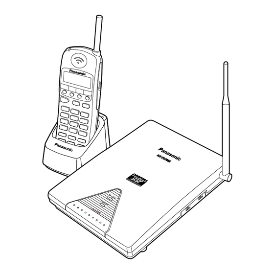
Panasonic KX-TD7895 Service Manual
Hide thumbs
Also See for KX-TD7895:
- Operating instructions manual (48 pages) ,
- Brochure & specs (2 pages) ,
- Specifications (7 pages)

Related Manuals for Panasonic KX-TD7895


Summary of Contents for Panasonic KX-TD7895
- Page 1 ORDER NO. KMS0101535C1 WIRELESS PHONE KX-TD7895 (for U.S.A.) SPECIFICATIONS 2001 Kyushu Matsushita Electric Co., Ltd. All rights reserved. Unauthorized copying and distribution is a violation of law.
-
Page 2: For Service Technicians
1. CAUTION Note: When you mention the serial number, write down all 11 digits. The serial number may be found the label affixed to the bottom of the unit. 2. FOR SERVICE TECHNICIANS ICs and LSIs are vulnerable to static electricity. When replacing, the following precautions will help prevent recurring malfunctions. - Page 3 3.2. CONNECTIONS OF HANDSET...
- Page 4 3.3. BASE UNIT...
- Page 5 4. DISASSEMBLY INSTRUCTIONS 4.1. BASE UNIT...
- Page 6 1. Remove the four screws (A), and remove the Bottom Cabinet.
- Page 7 2. Remove the Main Board from the Top Cabinet. 3. Remove the two screws (B), and remove the RF Unit from the Main Board.
- Page 8 4. Remove the screw (C), and remove the Antenna from the Top Cabinet. Remove the Panel (LED) and the Button (Locate) from the Top Cabinet. 4.2. HANDSET 1. Remove the Battery Cover sliding it in the direction of the arrow.
- Page 9 2. Take the Battery out of the Rear Cabinet after disconnecting the Connector.
- Page 10 3. Remove two Screws (D) from the Rear Cabinet.
- Page 11 4. Unfasten the Top hook after unfastening Both side hooks to Front Cabinet from Rear Cabinet. CAUTION: If you open the front cabinet too far, the Top hook may snap. 5. Remove three Terminal Plates from the Rear Cabinet.
- Page 12 6. Remove the Antenna from the Front Cabinet after removing the Screw (E).
- Page 13 7. Remove the RF unit from the Main Board.
-
Page 14: Adjustments (Handset)
8. Remove the Main Board from the Front Cabinet. 5. ADJUSTMENTS (HANDSET) 5.1. EQUIPMENT 1. Radio tester : Marconi Model 2295A or later. 2. DC Power Supply, capable of 3.9V DC supply at 2A. 3. Audio Cable : BNC end to alligator clip end. 4. - Page 15 and GND). 4. Connect a distortion meter (with AC voltmeter) to the SPK terminals (SP+) on the handset. 5. To Enter the Test Mode (1) Connect serial cable to main board. (TX, RX, GND, 3points) (2) Connect other side of serial cable to serial port of PC. (Dsub-9pins connector) (3) Start up the “Procomm plus“...
- Page 16 Item Adjustment Item Procedure Codec Input Level Adjust Codec Input Level (Test point : CDC-IN) to - Adjustment 12dBm by VR300. Speaker Output Level Adjust Speaker Output Level (Test point : SP+) to - Adjustment 28dBm by VR301. 6. CPU DATA 6.1.
- Page 17 Description High High-Z 19 Not USE 20 Not USE 21 Not USE 22 Not USE 23 Not USE 24 Not USE 25 Not USE 26 TEST NORMAL 27 POWER DOWN NORMAL POWER DOWN 28 BBIC INT NORMAL 29 AVCC 30 Not USE (JP1) NORMAL 31 Not USE (JP2) NORMAL...
- Page 18 58 POWER LED Description High High-Z 59 BBIC_PWRDWN O PWRDWN 60 BBIC_DEN 61 BBIC_ALE 62 BBIC_SCK 63 BBIC_RXD 64 BBIC_TXD 65 LCD CNT0 O NORMAL RESET 66 LCD CNT1 67 LCD CNT2 O NORMAL WRITE 68 LCD CNT3 O NORMAL CHIP SELECT 69 LCD DAT4...
- Page 19 Description High High-Z 1 /RES RESET NORMAL 2 XTAL 3 EXTAL 4 MD1 NORMAL 5 MD0 NORMAL 6 NMI NORMAL 7 Not USE (/ NORMAL STBY) 8 VCC2 9 Mic MUTE Mic ON Mic ON 10 RF POWER RF ON RF ON 11 VIBRATOR 12 VSS...
- Page 20 34 CHARGE...
- Page 21 Description High High-Z 35 TEMP_MONITOR I 36 CRNT_MNTR O NORMAL 37 BATT_MONITOR I 38 AVSS 39 CODEC_TXD 40 CODEC_RXD 41 CODEC_SCK 42 CODEC_DEN 43 RINGER 44 CHARGE_ON O NORMAL STOP 45 RINGER_VOL1 46 RINGER_VOL2 47 VCC1 48 F4_LED_R 49 F4_LED_G 50 F3_LED_R 51 F3_LED_G 52 F2_LED_R...
- Page 22 Description High High-Z 75 EEPROM_SCK 76 EEPROM_SI 77 EEPROM_SO 78 EXT_TXD 79 EXT_RXD 80 EXT_CLK 6.3. RF UNIT {IC501(PRL)}...
- Page 23 6.4. RF UNIT (FREQUENCY TABLE)
-
Page 24: Circuit Operation (Base Unit)
7. CIRCUIT OPERATION (BASE UNIT) 7.1. MAIN BOARD 7.1.1. POWER SUPPLY CIRCUIT The Voltage between 9V and 16V is supplied to the DC Jack from the AC adaptor. The Power for the RF Unit is supplied from IC251 and Q261. The Power for the Analog Circuit is supplied from Q101. - Page 25 Bell signal, IC107(57) repeats High/Low fluctuation and then D105 in use is flashed. The data signal indicating the Bell incoming is sent to the portable unit through the RF unit so the handset ringer is on. 7.1.3. LINE INTERFASE The line is looped when the IC107(46) becomes High and Q107 and Q100 are ON. The looped current flows through Q100 Q108 R180.
- Page 26 telephone line. Via the following path: RF unit IC106(24) IC106(11) C153 R193 C162 Q115 C159 R202 C110 Q103 R106 C187 Q108 Q100 D101 7.1.6. DTMF SIGNAL When the DTMF data from the portable unit is received, the DTMF signal is output from the IC105(23) and sent to the line.
- Page 27 STANDBY TALK [Normal] IC105(41) IC107(46) [Auto Answer] IC105(41) IC107(46) IC113(4) (OR) H : Hook (OFF Hook) 7.1.8. RESET CIRCUIT This circuit is used for transmission of a reset pulse to the CPU(IC107). Reset pulse is Low. 7.1.9. DATA COMMUNICATION CIRCUIT FUNCTION The data communication circuit serves the following function (in the EMSS mode):Information exchanger between the EMSS and Base Unit, key input information as well as data for the LED...
- Page 28 EMSS proprietary telephone will return an acknowledgement signal, to the EMSS. 1. Reception The data from the EMSS is received via the H and L line along the path shown below. H, L Line D104 T100 R114 Q106 IC104(6) IC105(37) 2.
-
Page 29: Circuit Operation (Handset)
8. CIRCUIT OPERATION (HANDSET) 8.1. MAIN BOARD 8.1.1. POWER SUPPLY CIRCUIT The power supply circuit consists of 4 regulators. IC314 supplies the power to the CPU(IC307). IC301, IC305 and IC308 are controlled by the CPU(IC307). Each output voltage is 3.0V. 8.1.2. - Page 30 The digital voice signal from the Base Unit is changed to a Analog signal by IC303 and sent to the speaker. 8.1.4. SENDING VOICE SIGNAL The Analog input signal from Microphone is changed to a digital signal. And sent to the Base Unit.
- Page 31 JT301 : ”High” Q309 : ON IC311(5) : “High“ IC311(3) : “High“ IC309(1) : “High“ IC307(7) : “High“ 8.1.6. CHARGING DETECTION If the Handset is put on the charger to recharge it, the DC voltage appears on "CHG+" terminal of battery connector JT301. PUT ON THE CHARGER Q309 ON IC307(34)
-
Page 32: Troubleshooting Guide
10. TROUBLESHOOTING GUIDE 10.1. NO VOICE RECEPTION 10.2. NO VOICE TRANSMISSION... - Page 33 10.3. NO LINK (BASE UNIT)
- Page 34 10.4. NO LINK (HANDSET) 10.5. SELF DIAGNOSIS ERROR(BASE UNIT) If you see the blinking of Power LED(red) in intervals of 1 second when you connect the AC adaptor to Base Unit, Self Diagnosis error is detected by CPU. The errors are occurred by following four reasons.
- Page 35 (1) RF unit error (2) EEPROM read write error (3) EEPROM stored data error (4) Codec IC error 10.6. SELF DIAGNOSIS ERROR(HANDSET) If you see the need repair X (X means ldigit NO.) on LCD display of Handset when you turn on the Power Switch, Self Diagnosis error is detected by CPU.
-
Page 36: How To Replace The Flat Package Ic
(3) EEPROM stored data error (4) Codec IC error (5) Sub Clock Oscillator error 11. HOW TO REPLACE THE FLAT PACKAGE IC If you do not have the special tools (for example: SPOT HEATER) to remove the SPOT HEATER’S Flat IC, if you have solder (large amount) a soldering iron and a cutter knife, you can easily remove IC’s even though large than 100 pin. - Page 37 Recommended power consumption is between 30 W to 40 W. Temperature of Copper Rod 662 ± 50°F (350 ± 10°C) (An expert may handle a 60~80 W iron, but beginner might damage foil by overheating.) - Flux HI115 Specific gravity 0.863 (Original flux should be replaced daily.) 11.2.
- Page 38 After removing the Flat IC and when attaching the new IC, remove any of the excess solder on the land using the soldering wire, etc. If the excess solder is not removed from the land, the IC will slip and not be attached properly. 11.3.
-
Page 39: Cabinet And Electrical Parts Location
12. CABINET AND ELECTRICAL PARTS LOCATION 12.1. BASE UNIT... - Page 40 12.2. HANDSET...
- Page 41 12.3. CHARGER...
-
Page 42: Accessories And Packing Materials
13. ACCESSORIES AND PACKING MATERIALS... -
Page 43: Replacement Parts List
14. REPLACEMENT PARTS LIST Note: 1. RTL (Retention Time Limited) The marking (RTL) indicates that the Retention Time is limited for this item. After the discontinuation of this assembly in production, the item will continue to be available for a specific period of time. The retention period of availability depends on the type of assembly... - Page 44 and the laws governing parts and product retention. At the end of this period, the assembly will no longer be available. 2. Important safety notice Components identified by the mark indicates special characteristics important for safety. When replacing any of these components, only use specified manufacture's parts.
- Page 45 Ref. No. Part No. Part Name & Description Remarks PCB1 PSWP1TD7894M MAIN BOARD ASS'Y(RTL) (ICS) IC100 PSVIXC612812 IC101 PQVIC61CC32N IC102 AN6183S IC103 C3EBDG000024 IC104 PQVIPD4011G IC105 MN150409KRP IC106 PSVIML7029MB IC107 PSWITD7895H IC110 C0CBACE00012 IC IC112 PQVITC7S08FR IC113 PQVITC7S32FR IC251 PQVIMC34063M IC (TRANSISTORS) Q100 2SA1625...
- Page 46 (CAPACITORS)
- Page 47 Ref. No. Part No. Part Name & Description Remarks C100 ECQE2224KF 0.22 C101 ECKD2H681KB 680p C102 ECKD2H681KB 680p C103 ECEA1HU3R3 C104 ECUV1C224KBV 0.22 C106 ECEA1EK470 C107 ECUV1H101JCV 100p C109 ECUV1C224KBV 0.22 C110 ECUV1C104KBV 0.1 C111 ECUV1H330JCV 33p C112 ECEA1EU221 C113 ECEA1CGE470 C114 ECUV1A105ZFV 1...
- Page 48 Ref. No. Part No. Part Name & Description Remarks C174 ECUV1A105ZFV 1 C176 ECUV1A105ZFV 1 C178 ECUV1H103KBV 0.01 C179 ECEA1EKA100 C181 ECUV1H101JCV 100p C182 ECUV1H103KBV 0.01 C183 ECUV1C683KBV 0.068 C184 ECEA1CKS100 C186 ECUV1E393KBV 0.039 C187 ECUV1C104KBV 0.1 C188 PQCUV1C104ZF 0.1 C189 PQCUV1C104ZF 0.1 C191...
- Page 49 Ref. No. Part No. Part Name & Description Remarks R117 ERJ3GEYJ103 R118 ERJ3GEYJ103 R119 ERJ3GEYJ103 R120 ERJ3GEY0R00 R121 ERJ3GEYJ103 R122 ERJ3GEYJ473 R123 ERJ3GEYJ104 100k R125 ERJ3GEYJ103 R126 ERJ3GEYJ101 R127 ERJ3GEYJ154 150k R128 ERJ3GEYJ472 4.7k R129 ERJ3GEYJ101 R130 ERJ3GEYJ153 R132 PQ4R10XJ681 R134 ERJ3GEYJ473 R137...
- Page 50 Ref. No. Part No. Part Name & Description Remarks R202 ERJ3GEYJ183 R212 ERJ3GEY0R00 R215 ERJ3GEYJ104 100k R217 ERJ3GEYJ682 6.8k R220 ERJ3GEYJ103 R226 ERJ3GEY0R00 R231 ERJ3GEYJ471 R234 ERJ3GEY0R00 R236 ERJ3GEY0R00 R239 ERJ3GEY0R00 R241 ERJ3GEYJ104 100k R242 ERJ3GEYJ560 R251 ERJ3GEYJ1R0 R252 ERJ3GEYJ1R0 R253 ERJ3GEYJ1R0 R254...
- Page 51 Ref. No. Part No. Part Name & Description Remarks PC100 PQVIPC814K PHOTO COUPLER 14.1.3. RF UNIT Ref. No. Part No. Part Name & Description Remarks PCB2 PSWP2TD7894M RF UNIT PARTS ASS'Y(RTL) (IC) IC501 PQVILXT810TC (CONNECTOR) CN501 K1KB20A00032 CONNECTOR,20P (CAPACITORS) C501 ECUV1H090DCV 9p C502 ECUV1H090DCV 9p...
- Page 52 Ref. No. Part No. Part Name & Description Remarks R503 ERJ3GEYJ332 3.3k R504 D0GB224ZA002 220k R505 MQLRE1N0DF2 COIL R522 ERJ3GEYJ104 100k (COILS) L502 MQLRE5N6JF2 COIL L504 MQLRE47NJF2 COIL L505 MQLRE47NJF2 COIL L506 ECUV1H010CCV 1P(CAPACITOR) L507 MQLRE22NJF2 COIL (CERAMIC FILTER) FIL501 J0D9156B0002 CERAMIC FILTER (TRANSFORMER)
- Page 53 Ref. No. Part No. Part Name & Description Remarks PSHR1219Z SPACER PSHX1164Z COVER LNY162C03F 14.2.2. MAIN BOARD Ref. No. Part No. Part Name & Description Remarks PCB3 PSWP2TD7895M MAIN BOARD PARTS ASS'Y(RTL) (ICS) IC301 PSVIRN5RF30B IC302 PQVINJM2135V IC303 PSVIML7029MB IC304 C0EBF0000063 IC305 PSVIRN5RF30B...
- Page 54 Ref. No. Part No. Part Name & Description Remarks D305 LNJ308G8JRA D306 LNJ308G8JRA D307 LNJ308G8JRA D308 LNJ308G8JRA D309 LNJ308G8JRA D311 PQVDRB751H4 DIODE(SI) D312 LNJ308G8JRA D313 LNJ308G8JRA D314 PSVDLS22BB1U DIODE(SI) D315 PSVDLS22BB1U DIODE(SI) D316 PSVDLS22BB1U DIODE(SI) D317 PSVDLS22BB1U DIODE(SI) D318 LNJ115W8PRA DIODE(SI) D319 LNJ115W8PRA...
- Page 55 Ref. No. Part No. Part Name & Description Remarks C335 ECUV1A105ZFV 1 C336 ECST0JY106 C337 ECST0JY106 C338 ECUV1A105ZFV 1 C340 PQCUV1C104ZF 0.1 C341 ECUV1C473KBV 47000P C342 F3G0G1070002 C343 ERJ3GEYJ103 10k (RESISTOR) C344 ECUV1H100DCV 10p C345 ECUV1H100DCV 10p C348 ECUV1H220JCV 22p C349 ECUV1H220JCV 22p C350...
- Page 56 Ref. No. Part No. Part Name & Description Remarks R319 ERJ3GEYJ391 R320 ERJ3GEYJ101 R321 ERJ3GEYJ391 R322 ERJ3GEYJ101 R323 ERJ3GEYJ391 R324 PQ4R10XJ220 R325 ERJ3GEYJ104 100k R326 ERJ3GEYJ274 270k R327 ERJ3GEYJ182 1.8k R328 ERJ3GEYJ474 470k R329 ERJ3GEYF204 200k R330 ERJ3GEYF304 300k R331 ERJ3GEYF204 200k R332...
- Page 57 Ref. No. Part No. Part Name & Description Remarks R389 ERJ3GEYJ104 100k R390 PQLQR1RS241T COIL R391 ERJ3GEYJ101 R392 ERJ3GEYJ103 R393 PQLQR1RS241T COIL ERJ3GEY0R00 (BATTERY TERMINALS) JT300 PQJT10090Z BATTERY TERMINAL JT301 PQJT10090Z BATTERY TERMINAL JT302 PQJT10090Z BATTERY TERMINAL (SWITCH) SW300 ESD165206 SWITCH (THERMISTOR) TH300...
- Page 58 Ref. No. Part No. Part Name & Description Remarks PCB4 PSWP4TD7894M RF UNIT PARTS ASS'Y(RTL) (IC) IC501 PQVILXT810TC (CONNECTOR) CN501 K1KB20A00032 CONNECTOR C501 ECUV1H090DCV 9p C502 ECUV1H090DCV 9p C503 PQCUV1C104ZF 0.1 C504 PQCUV1C104ZF 0.1 C505 ECUV1H220JCV 22p C506 ECST0JY226 C507 PQCUV1C104ZF 0.1 C508 ECUV1H220JCV 22p...
- Page 59 Ref. No. Part No. Part Name & Description Remarks L505 MQLRE47NJF2 COIL L507 MQLRE22NJF2 COIL L508 MQLRE10NJF2 COIL (CERAMIC FILTER) FIL501 J0D9156B0002 CERAMIC FILTER (TRANSFORMER) T501 J2GE00000008 TRANSFORMER (CRYSTAL OSCILLATOR) X501 H0J240500009 CRYSTAL OSCILLATOR 14.3. CHARGER 14.3.1. CABINET AND ELECTRICAL PARTS Ref.
- Page 60 Ref. No. Part No. Part Name & Description Remarks PCB5 PSWP5TD7894M MAIN BOARD ASS'Y (RTL) (ICS) IC601 PQVINJ2360D IC602 PSVITA75S01F (TRANSISTORS) Q641 2SB1218A TRANSISTOR(SI) (DIODES) D621 MA738 DIODE(SI) D622 MA738 DIODE(SI) D642 MA1Z062 DIODE(SI) D643 MA111 DIODE(SI) (JACK) CN601 PSJJ1B002Z JACK (CAPACITORS) C601...
-
Page 61: Block Diagram
14.4. ACCESSORIES AND PACKING MATERIALS Ref. No. Part No. Part Name & Description Remarks PQLV1 AC ADAPTOR XWG35FY WASHER PQHE5004Z SCREW PQJA48W CORD,TEL PSKE1040Z BELT HOLDER PSKE1036Z HANGER PQKL25Y STAND PSQX2106Z INSTRUCTION BOOK PSQW1531Z LEAFLET PSQA2325Z LEAFLET(FOR HANDSET) PSPK1831Z GIFT BOX PSPN1124Z ACCESSORY BOX PSPD1147Z... - Page 62 17.2. BASE UNIT(RF) 17.3. HANDSET(MAIN) 17.3.1. CONPONENT VIEW 17.3.2. BOTTOM VIEW 17.4. HANDSET(RF) 17.5. CHARGER BOARD A KXTD7895...
Need help?
Do you have a question about the KX-TD7895 and is the answer not in the manual?
Questions and answers