
Subscribe to Our Youtube Channel
Related Manuals for Motorola DSP96002ADM


Summary of Contents for Motorola DSP96002ADM
- Page 1 DSP96002ADM User’s Manual Motorola, Incorporated Semiconductor Products Sector Wireless Division 6501 William Cannon Drive West Austin, TX 78735-8598...
- Page 2 Motorola assume any liability arising out of the application or use of any product or circuit, and specifically disclaims any and all liability, including without limitation consequential or incidental damages. “typical” parameters which may be provided in Motorola data sheets and/or specifications can and do vary in different applications and actual performance may vary over time.
-
Page 3: Table Of Contents
Connecting the DSP96002ADM to the PC and Power ..1-8 USING THE DSP96002ADM ......1-8 SECTION DSP96002ADM TECHNICAL SUMMARY. - Page 4 LIST OF FIGURES Figure 1-1 DSP96002ADM Key Component Layout ..... . 1-6 Figure 1-2 Application Development ........1-8 Figure 2-1 DSP96002ADM Functional Block Diagram .
- Page 5 DSP96002ADM Default Jumper Options ..... 1-7 Table 2-1 DSP96002ADM Jumper Functions ......2-7 Table 2-2 Operating Mode Selection .
- Page 6 DSP96002ADMUM/AD, Preliminary MOTOROLA...
-
Page 7: Section 1 Quick Start Guide
SECTION 1 QUICK START GUIDE MOTOROLA DSP96002ADMUM/AD, Preliminary... - Page 8 Connecting the DSP96002ADM to the PC and Power ..1-8 USING THE DSP96002ADM......1-8...
-
Page 9: Overview
Quick Start Guide Overview OVERVIEW The Motorola Application Development System is a tool used to design and test complex software applications and hardware products using a specific Motorola DSP chip. The related Application Development Modules (ADMs) contain the DSP chip and related hardware used for bench development and test. -
Page 10: What You Need To Supply
INSTALLATION PROCEDURE Installation requires the following steps: 1. Using information provided in the Motorola Application Development System User’s Manual, install the Motorola Application Development System in the host computer. 2. Prepare the DSP96002ADM board 3. Connect the board to the external Command Converter card... -
Page 11: Preparing The Dsp96002Adm
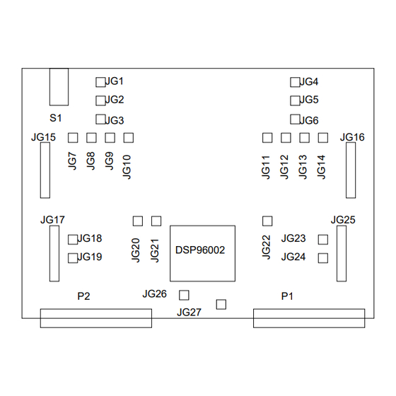
– Always transport sensitive components in anti-static packaging. Locate the twenty-seven jumper blocks JG1–JG27 on the DSP96002ADM board, as shown in Figure 1-1 on page 1-6. Table 1-1 describes the default jumper and switch settings when shipped from the factory. -
Page 12: Figure 1-1 Dsp96002Adm Key Component Layout
Quick Start Guide Installation Procedure JG15 JG16 JG17 JG25 JG18 JG23 DSP96002 JG19 JG24 JG26 JG27 Figure 1-1 DSP96002ADM Key Component Layout DSP96002ADMUM/AD, Preliminary MOTOROLA... -
Page 13: Table 1-1 Dsp96002Adm Default Jumper Options
Quick Start Guide Installation Procedure Table 1-1 DSP96002ADM Default Jumper Options Jumper Place Jumpers Comment Block between Pins 1–2 1–2 Exit reset in Mode 0 1–2 1–2 IRQA pass through reset logic 1–2 IRQB pass through reset logic 1–2 IRQC pass through reset logic 1–2... -
Page 14: Connecting The Dsp96002Adm To The Pc And Power
Connecting the DSP96002ADM to the PC and Power Figure 1-2 shows the interconnection diagram for connecting the PC and the external power supply to the DSP96002ADM board. Using the instructions in the Application Development System User’s Manual, connect the Command Converter to the ADM board. -
Page 15: Section 2 Dsp96002Adm Technical Summary
SECTION 2 DSP96002ADM TECHNICAL SUMMARY MOTOROLA DSP96002ADMUM/AD, Preliminary... - Page 16 EXTERNAL/INTERNAL RESET INPUT ....2-5 CONFIGURING THE DSP96002ADM.....2-6 2.4.1...
-
Page 17: Dsp96002Adm Description And Features
DSP96002ADM Description and Features DSP96002ADM DESCRIPTION AND FEATURES The DSP96002ADM has various options to facilitate evaluation of the different features of the chip. These options are outlined in this chapter. Figure 2-1 on page 2-4 shows a block diagram of the DSP96002ADM architecture. To achieve zero wait accesses memory decoding is minimal, therefore memory may overlap into other address blocks within a $20000000 address space. -
Page 18: Figure 2-1 Dsp96002Adm Functional Block Diagram
Memory Decoder Decoder Program/ Program/ X data/ X data/ Y data Y data SRAM SRAM Program Program EPROM EPROM Port A Data Port B Data Port A Address Port B Address Figure 2-1 DSP96002ADM Functional Block Diagram DSP96002ADMUM/AD, Preliminary MOTOROLA... -
Page 19: Dsp96002 Description
DSP96002ADM Technical Summary DSP96002 Description DSP96002 DESCRIPTION A full description of the DSP96002, including functionality and user information is provided in the following documents included as a part of this kit (either as printed copies or on the documentation CD-ROM): •... -
Page 20: Configuring The Dsp96002Adm
DSP96002ADM Technical Summary Configuring the DSP96002ADM CONFIGURING THE DSP96002ADM There are twenty-seven jumper options on the DSP96002ADM. Figure 2-2 illustrates the physical locations of jumpers JG1 to JG27. Table 2-1 on page 2-7 defines the different Jumper Group functions. JG15... -
Page 21: Table 2-1 Dsp96002Adm Jumper Functions
DSP96002ADM Technical Summary Configuring the DSP96002ADM Table 2-1 DSP96002ADM Jumper Functions Jumper Function Block Selects operating mode out of reset IRQ configuration JG10 JG11 EPROM size configuration JG12 JG13 JG14 JG15 JG16 JG17 SRAM partition configuration (with JG25) JG18 SRAM address space decoding configuration (with JG23) -
Page 22: Operating Mode Selection
DSP96002ADM Technical Summary Configuring the DSP96002ADM 2.4.1 Operating Mode Selection Jumpers JG1 to JG3 are used to select one of eight operating modes in which the DSP96002 exits reset. The ADM is factory configured for MODE 0. In MODE 0, the internal program memory occupies the lower portion of the program memory space. -
Page 23: External Irqa/Irqb/Irqc Input Path
DSP96002ADM Technical Summary Configuring the DSP96002ADM 2.4.2 External IRQA/IRQB/IRQC Input Path The paths for the external input signals MODA/IRQA, MODB/IRQB, and MODC/IRQC are selected by JG4, JG5, and JG6, respectively. These jumpers allow the designer to use the multiplexed function of these inputs, or to select only the interrupt function of these external signals. -
Page 24: Dsp96002 Port A/B User Eprom Decoders
DSP96002ADM Technical Summary Configuring the DSP96002ADM 2.4.3 DSP96002 Port A/B User EPROM Decoders Port A and B both contain sockets that accommodate EPROMs of various densities. Six types of EPROMs, ranging from 2 K × 8 to 64 K × 8, may be installed in the sockets. The lower density EPROMs come in 24-pin packages while the higher density EPROMs are available in 28-pin packages. -
Page 25: Dsp96002 Port A/B User Sram Decoder/Partitions
4 or 256 K 4 device will work with the DSP96002ADM. The SRAM decoder does not have bus arbitration signals as qualifiers; therefore, any processor that becomes the bus master may directly access the SRAMs. This is useful in shared memory configurations. The SRAM address lines are buffered to decrease the DSP96002 address bus loading. -
Page 26: Table 2-6 Port A/B User Sram Decoder
DSP96002ADM Technical Summary Configuring the DSP96002ADM Table 2-6 Port A/B User SRAM Decoder OPTION JG18 / JG23 SRAM MEMORY BLOCK 1–2, 3–4, 5–6 $00000000–$1FFFFFFF 3–4, 5–6 $20000000–$3FFFFFFF 1–2, 5–6 $40000000–$5FFFFFFF 5–6 $80000000–$9FFFFFFF No jumpers $E0000000–$FFFFFFFF Table 2-7 Port A/B User SRAM Selection Jumpers for 64 K ×... -
Page 27: Clock Input Selection
DSP96002ADM Technical Summary Configuring the DSP96002ADM 2.4.5 Clock Input Selection Using jumper JG20, the user can select either the ADM U21 clock output or an external clock input via P1 connector P1-C30 pin as the DSP96002 clock source. The ADM clock is buffered via U6-3 (74AS08 AND Gate), which provides a current source of –2 mA and a... -
Page 28: Dsp96002 Adm Connector Descriptions
DSP96002ADM Technical Summary DSP96002 ADM Connector Descriptions DSP96002 ADM CONNECTOR DESCRIPTIONS Table 2-9 DSP96002 ADM P1/J3 Port A Connector PIN # ROW A ROW B ROW C aD00 aD25 aA10 aD01 aD26 aA09 aD02 aD27 aA08 aD03 aD28 aA07 aD04... -
Page 29: Table 2-10 Dsp96002 Adm P2/J4 Port B Connector
DSP96002ADM Technical Summary DSP96002 ADM Connector Descriptions Table 2-9 DSP96002 ADM P1/J3 Port A Connector (Continued) PIN # ROW A ROW B ROW C +5 V +5 V +5 V Note: (n/c) means that the pin is not connected.. Both P1 and J3 are plugs. - Page 30 DSP96002ADM Technical Summary DSP96002 ADM Connector Descriptions Table 2-10 DSP96002 ADM P2/J4 Port B Connector (Continued) PIN # ROW A ROW B ROW C bD28 MODC/IRQC bA28 bD29 RESET bA29 bD30 bA30 bD31 +5 V bA31 Note: (n/c) means that the pin is not connected. Both P2 and J4 are plugs.
- Page 31 APPENDIX A DSP96002ADM SCHEMATICS MOTOROLA DSP96002ADMUM/AD...
- Page 32 DSP96002ADM Schematics DSP96002ADMUM/AD MOTOROLA...
- Page 33 MOTOROLA DSP96002ADMUM/AD...
- Page 34 DSP96002ADMUM/AD MOTOROLA...
- Page 35 MOTOROLA DSP96002ADMUM/AD...
- Page 36 DSP96002ADMUM/AD MOTOROLA...
- Page 37 MOTOROLA DSP96002ADMUM/AD...
- Page 38 DSP96002ADMUM/AD MOTOROLA...
- Page 39 MOTOROLA DSP96002ADMUM/AD...
- Page 40 A-10 DSP96002ADMUM/AD MOTOROLA...
- Page 41 MOTOROLA DSP96002ADMUM/AD A-11...
- Page 42 A-12 DSP96002ADMUM/AD MOTOROLA...
- Page 43 MOTOROLA DSP96002ADMUM/AD A-13...
- Page 44 A-14 DSP96002ADMUM/AD MOTOROLA...
- Page 45 APPENDIX B DSP96002ADM BILL OF MATERIALS MOTOROLA DSP96002ADMUM/AD, Preliminary...
- Page 46 DSP96002ADM Bill of Materials DSP96002ADMUM/AD, Preliminary MOTOROLA...
-
Page 47: Dsp96002Adm-Electrical Parts List Rev. 1.8 --10/20/93
DSP96002ADM Bill of Materials DSP96002ADM—ELECTRICAL PARTS LIST REV. 1.8 --10/20/93 Description Ref. Designators Vendor Part # Integrated Circuits DSP96002 Motorola WS57C191B35D U1–U4, U8–U11 WaferScale Integration MC1455P1 Motorola 74FACT00 U5, U6, U7 Motorola 74F138 U42, U43 Motorola 74F32 U41, U44 Motorola... -
Page 48: Dsp96002Adm-Hardware Parts List Rev. 1.8 --10/20/93
DSP96002ADM Bill of Materials DSP96002ADM—HARDWARE PARTS LIST REV. 1.8 --10/20/93 Description Ref. Designator Vendor Part # Jumpers 2 row × 12 Bergstiks JG15–JG17, JG25 R.N. NSH-12DB-S2-TG30 2 row × 2 Bergstiks JG20 R.N. NSH-04DB-S2-TG30 (18) 1 row × 3 Bergstiks JG1–JG14, JG21, JG22,...
Need help?
Do you have a question about the DSP96002ADM and is the answer not in the manual?
Questions and answers