Advertisement
Quick Links
Advertisement

Related Manuals for TTI 1906


Summary of Contents for TTI 1906
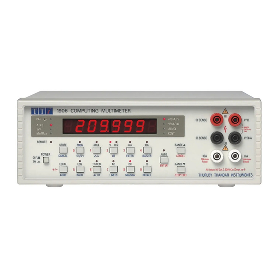
- Page 1 1906 Multimeter Service Manual Part Number 48511-1110 Iss.2...
-
Page 2: Table Of Contents
Table of Contents Specification Safety General Overview & Principles Operation Detailed Circuit Operation Calibration Parts List Circuit Diagrams... -
Page 3: Specification
Specification Accuracy Accuracies apply for 1 year 18°C to 26°C. Temperature coefficient outside these limits is <0.1x quoted range accuracy per °C. Warm-up time to rated accuracy is 1 hour. DC VOLTS Range Accuracy Input Impedance Max Input 200Mv 0.017% + 3D 1kV DC or 10MΩ... - Page 4 AMPS Range Accuracy Voltage Burden Max Input 200uA 0.08% + 12D 1A,300V 0.08% + 12D 300mV max fuse protected 20mA 0.08% + 12D 200mA 0.08% + 12D up to 2000mA 0.06% + 10D 650mV max 10A, 300V above 2000mA 0.12% + 10 fuse protected TRMS AC AMPS Range...
- Page 5 Displays measurement in dB relative to 1V, 1mA, 1kOhm or user entered value, or in dBm. Ax+B: Linear scaling of results, with offset. Limits: Reading displayed with 'H','L',or'P' (pass) with respect to user-defined high and low limits. Min/Max: Minimum and maximum reading stored. Data Logger: Manual or automatic storage of 100 measurements.
-
Page 6: Safety
Safety When operating the instrument with the covers off the users attention is drawn to the fact that the measurement circuit analogue common is capable of being driven up to 1kV above earth ground. All measurement circuits are therefore potentially hazardous, including the CPU section of the main board and the display/keyboard mounted behind the front panel. -
Page 7: General Overview & Principles Operation
General Overview & Principles Operation (refer to the block diagram fig.1) The input signal conditioning includes the input attenuator, current shunts, and analogue switches required for range switching. All analogue switches are either CMOS gates or MOSFETs. By software calibrating every meter range high precision components are avoided, the only requirement is stability. -
Page 8: Detailed Circuit Operation
Detailed Circuit Operation The following sections describe the detailed operation of the circuit blocks outlined in the general overview. Refer to the main circuit diagrams where information is not presented on simplified schematics. Measurement Control Signals and Signal Drivers The CPU is responsible for setting up all the measurement signal paths implemented using CMOS analogue gates and MOSFETS. - Page 9 current is fed to the bottom element of the attenuator via IC1-A in the 20V range and via IC1-D plus the appropriate gate in IC2 in the 200V and 1kV ranges. The voltage across the bottom of the attenuator is sensed via IC1-C or IC1-B and IC2. The gate selection in IC2 is controlled by CTRL6 and CTRL7, which select the gates according to a binary code with CTRL6 the LSB.
- Page 10 Fig. 2 - AC Volts I/P - Simplified Schematic Input Signal Conditioning‚ - AC Volts Attenuation‚ (refer to simplified schematic fig. 2) The AC voltage readings require one sub-reading. The LO terminal is sensed via AG and is measured during the regular reference updates. IC4-A is therefore switched on permanently except during the reference sub-readings.
- Page 11 In the ranges 2V, 20V and 200V F7 is turned on and IC2 selects the feedback for IC51. As for the DC attenuator the measurement signal is gated via IC1-D and the sense is routed via IC1-B to the amplifier input. IC8-B and IC-D are turned off so that R78 is not in circuit. IC3-B is turned off so that R120 is not in circuit.
- Page 12 Input Signal Conditioning‚ - Resistance Measurement and Continuity Check (refer to simplified schematic fig. 3) Resistance measurements are made using a ratiometric method. The same measurement current is passed through a reference resistor and the resistance to be measured (X). For each complete reading a sub-reading is made of the voltage at each end of the reference resistor (REF HI and REF LO) and at each end of the unknown resistance (X HI and X LO).
- Page 13 Because the CPU input pin used by CONT DET can also be used as the processor HALT bar input it is necessary to ensure at power up that the CONT DET signal is held high until the power up routine has time to change the function from HALT bar to input port. For this reason RES bar hold Q16 turned on at power up via R102 and C61 ensures that CONT DET does not fall before the software has had time to set up the input port.
- Page 14 Fig. 5 - A/D Converter Waveforms (not to scale) The A/D Converter (refer to simplified schematic fig. 4 and waveform diagram fig.5) IC40 provides a x1 or x10 input buffer to the converter. R10 filters out HF noise picked up on the extremely high impedance node feeding IC40.
- Page 15 transistor array and IC17-A is a common emitter pair wired to form a diode switch. At the end of the conversion period pin 2 is pulled high to divert the measurement current from the integrator. The main conversion period is determined by the CPU control signal CB ENABLE, whose state is changed within the CPU's NMI routine, which is initiated by the low going edge of the 600Hz signal generated in IC14.
- Page 16 Buzzer The programmable buzzer is driven by a square wave from IC14, buffered by Q17. The buzzer is turned on by a high CTRL19‚ signal. Power Supply The power supply consists of two sets of linear regulators driven from the mains transformer. One set of regulators, IC41,IC42, IC43 and IC50, supplies the measuring circuitry which requires to be completely floating relative to earth ground.
- Page 17 The main display is driven one digit at a time by open collector driver IC39 under control of latch IC38. The LEDs are arranged in a row and column matrix with the three rows anode driven from IC37 and the columns driven by the digit driver, IC39. The keyboard is scanned using the digit multiplex drive signals from IC38.
- Page 18 GPIB Interface (refer to both the main CPU/Keyboard/Display and GPIB circuit diagrams) The GPIB interface operates via the RS232 interface. The source and destination of the RS232 signals are selected on the main board as follows. IC26-B is used as a logic gate to inhibit RS232 data reaching the GPIB board when RS232 is selected.
- Page 19 1/0 = high/low state A = active, toggling according to measurement sub-reading x = not set according to function/range Fig. 6 Table of Control Signals vs. Function/Range...
-
Page 20: Calibration
Calibration The instrument is software calibrated and retains its calibration constants in EEPROM. The calibration procedure is programmed into the ROM and simply has to be stepped through by front panel key presses or by remote interface commands. The magnitude of the required calibration signal for each range and function is also programmed into the ROM and is displayed as a calibration prompt at each step. - Page 21 left hand corner of the front panel using a suitable narrow tool. The switch should be made to latch in. The instrument is then switched on and the display shows 'DeF cAL'. Pressing the STORE‚ key stores the default calibration constants in EEPROM, overwriting any that may already have been there.
- Page 22 response which is 'P' if the step calibration was successful and 'F'if it failed. Note that in GPIB or addressed RS232 operation the meter is held up until the response is taken by the controller. If the response is 'F' it is necessary to send another STEPCAL‚ in order to move to the next calibration step.
- Page 23 DC Volts Calibration Step No. Input Value Comments 000.000mV s/coni/p 0.00000V ditto 00.0000V ditto +200.000mV +2.00000V -2.00000V +20.0000V +200.000V +1000.00V AC Volts Calibration Step No. Input Value Comments 200.000mV500Hz 40.000mV500Hz 2.00000V500Hz 0.40000V500Hz 20.0000V500Hz 200.000V500Hz 750.00V500Hz DC Amps Calibration Step No. Input Value Comments 000.000mA...
- Page 24 Remote Calibration Commands start calibration of DC Volts function start calibration of DC Amps function A10DC start calibration of DC 10Amps function start calibration of AC Volts function start calibration of AC Amps function A10AC start calibration of AC 10Amps function OHMS start calibration of Ohms function STEPCAL...
-
Page 25: Parts List
Parts List PCB ASSY MAIN - (44812-0540) Part Number Description Position 20030-0263 WASHER M3 ZPST SCREEN LOWER/SCREEN SPACERS 20037-0301 WASHER M3 SHK/PROOF ZPST SCREEN LOWER/SCREEN SPACERS 20210-0101 NUT M3 ZPST SCREEN LOWER/SCREEN SPACERS 20234-0027 SCREW M3 X 6 PNHDPZ ZPST SCREEN SPACERS, PJ3 22010-0610 BATTERY 3V LITH 20MM BUTTON... - Page 26 PCB ASSY MAIN - (44812-0540) continued/… Part Number Description Position 23185-4560 RES 560KJ W25CF RD25S B/R 23185-5100 RES1M0J W25CF RD25S B/R R10,48,67,96,106 23185-5220 RES2M2J W25CF RD25S B/R 23185-6100 RES10MJ W25CF RD25S B/R R32,115,116 23187-1300 RES 300RJ W25CF RD25S B/R 23187-1620 RES 620RJ W25CF RD25S B/R 23187-2510 RES5K1J W25CF RD25S B/R...
- Page 27 PCB ASSY MAIN - (44812-0540) continued/… Part Number Description Position 23386-9201 VARISTOR V1,2,3,4 23388-9103 THERMISTOR PTC1 23427-0254 CAP1N0K 100V CER MED K P2.5 23427-0268 CAP22PG 100V CER NPO P2.5 23427-0328 CAP10PC63V CER RD870-6NPO1 23427-0357 CAP33PG63V CER N150 P2.5 23427-9206 CAP15PG 100V CER NPO P2.5 C38,39 23557-0647 CAP 10U 35V ELEC RE2 P2...
- Page 28 PCB ASSY MAIN - (44812-0540) continued/… Part Number Description Position 27106-0506 IC LM324N IC20-24, 46 27106-0624 IC AD711JN IC10,51 27106-0626 IC AD548JN IC40 27106-0704 IC MC34184P IC11 27160-0009 IC V/REG 7805 TO220 IC43,44 27160-0011 IC V/REG 78L05 TO92 IC50 27160-0012 IC V/REG 79L05 TO92 IC45 27160-0013...
- Page 29 PCB ASSY KEYBOARD ASSEMBLY (44812-0550) Part Number Description Position 20105-0510 INSERT THREADEDKF2-M3-ET 22225-0220 SWITCH PUSH/PUSH 22226-0140 KEYSWITCH DARK GREY SW2-16 22573-0056 HEADER 16 WAY STR SIL FOR DISP1,2 23185-0000 RES ZERO OHM LINKS 23185-0330 RES33RJ W25CF RD25S B/R R81-88 23185-0820 RES82RJ W25CF RD25S B/R R25,26,27 23185-3100...
- Page 30 REAR PANEL ASSY - (46812-0500) continued/… Part Number Description Position 20661-0221 SPACER Hex M3 x 20NPBR REAR PANEL/TRANSFORMER 22115-0240 TRANSFORMER 22300-9301 FUSEHOLDER Panel Mounting FOR FS1 22315-9401 FUSE 1A Fast Blow HBC 22520-0140 AC RECEP FUSED C19271 MS3-DPS 22520-0500 FUSE DRAWER 230/115 CL19274 22538-9404 BOOT INS FOR FUSED IEC SKT 22575-0203...
- Page 31 CASE PARTS Part Number Description Postion 10220-0100 GROMMET STRIP HEAT SCREEN UPPER, SCREEN LOWER RECOVERABLE 10232-0305 SLEEVE H20 X 20MML BLACK 20010-0253 RIVET SNAP-LOCK PLSTC 8x2.5MM FEET 20030-0263 WASHER M3 ZPST REGULATORS, SCREEN LOWER, PCB/SCREEN SPACERS 20030-0264 WASHER M2.5 ZPST FEET 20037-0301 WASHER M3 SHK/PROOF I/T ZPST...
- Page 32 CASED PARTS continued/… Part Number Decription Position 37541-0840 LABEL REAR PANEL MAINS FUSE 48581-1070 INSTRUCTION BOOK 48581-1071 ADDENDUM TO INSINS BOOK 58231-0050 TEST LEAD SET - DMM SAFETY PCB ASSY GPIB INTERFACE (44812-0560) Part Number Description Position 20030-0263 WASHER M3 ZPST INSULATOR/PCB 20038-9501 WASHER M3 SPRING...
- Page 33 Manufacturing Changes From December 1995 a number of changes were made to improve performance, particularly the settling time on AC measurements, and to ensure full compliance with EMC and LVD Directives. The main pcb became Issue 4, the IEEE interface assembly used the same pcb but without IC8 and with a different cable assembly, and the transformer was changed.
-
Page 34: Circuit Diagrams
Circuit Diagrams Circuit Diagram – Main Board – Input Signal Conditioning and A/D Converter. Circuit Diagram – Main Board – CPU Section, Keyboard and Display. Circuit Diagram – GPIB Interface Board. - Page 38 Thurlby Thandar Instruments Ltd Glebe Road, Huntingdon, Cambridgeshire PE29 7DR, England Telephone: (44) 01480 412451 Fax: (44) 01480 450409 e mail: sales@tti-test.com web site: www.tti-test.com Book Part No. 48581-1110 Issue 2...
Need help?
Do you have a question about the 1906 and is the answer not in the manual?
Questions and answers