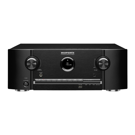
Marantz SR5006 Service Manual
Av surround receiver
Hide thumbs
Also See for SR5006:
- Owner's manual (146 pages) ,
- Model information (23 pages) ,
- Getting started manual (16 pages)
Table of Contents
Advertisement
Service
Manual
• For purposes of improvement, specifications and design are subject to change without notice.
• Please use this service manual with referring to the operating instructions without fail.
• Some illustrations using in this service manual are slightly different from the actual set.
S0408-0V04DM/DG1111
SR5006
Copyright 2011 D&M Holdings Inc. All rights reserved.
WARNING: Violators will be prosecuted to the maximum extent possible.
SR5006 /
AV Surround Receiver
U1B,K1B
s
N1SG
,N1B
s
s
Ver. 4
Please refer to the
MODIFICATION NOTICE.
Advertisement
Table of Contents

Related Manuals for Marantz SR5006


Summary of Contents for Marantz SR5006
- Page 1 Service SR5006 / U1B,K1B N1SG ,N1B Manual AV Surround Receiver • For purposes of improvement, specifications and design are subject to change without notice. • Please use this service manual with referring to the operating instructions without fail. • Some illustrations using in this service manual are slightly different from the actual set.
-
Page 2: Table Of Contents
CONTENTS SAFETY PRECAUTIONS ............4 SCHEMATIC DIAGRAMS ............106 7CH-AMP UNIT (1/2) ............106 NOTE FOR SCHEMATIC DIAGRAM .........5 7CH-AMP UNIT (2/2) ............107 TECHNICAL SPECIFICATIONS ..........6 SPK UNIT ................108 DIMENSION ................6 SMPS UNIT ................109 CAUTIONS IN SERVICING ............7 REG UNIT ................110 Initializing AV Surround Receiver ..........7 SIDE_CNT UNIT .............. - Page 3 Parts for your equipment are generally available to our National Marantz Subsidiary or agent. ORDERING PARTS : Parts can be ordered either by mail or by Fax.. In both cases, the correct part number has to be specified.
-
Page 4: Safety Precautions
SAFETY PRECAUTIONS The following items should be checked for continued protection of the customer and the service technician. LEAKAGE CURRENT CHECK Before returning the set to the customer, be sure to carry out either (1) a leakage current check or (2) a line to chassis resistance check. -
Page 5: Note For Schematic Diagram
NOTE FOR SCHEMATIC DIAGRAM WARNING: Parts indicated by the z mark have critical characteristics. Use ONLY replacement parts recommended by the manufacturer. CAUTION: Before returning the set to the customer, be sure to carry out either (1) a leakage current check or (2) a line to chassis resistance check. If the leakage current exceeds 0.5 milliamps, or if the resistance from chassis to either side of the power cord is less than 460 kohms, the set is defective. -
Page 6: Technical Specifications
TECHNICAL SPECIFICATIONS n Audio Section n Tuner section • Power amplifier [FM](Note: μV at 75 Ω, 0 dBf = 1 x 10 –15 Rated output : Receiving Range (for U model) : [FM] 87.5 MHz – 107.9 MHz [AM]520 kHz – 1710 kHz Front : Receiving Range (for N, K model) : 100 W + 100 W (8 Ω, 20 Hz –... -
Page 7: Cautions In Servicing
DISPLAY ZONE SELECT Service Jig When you repair the printing board, you can use the following JIG (Extension cable kit). Please order it from Marantz Official Service Distributor in your region if necessary. 8U-110084S EXTENSION UNIT KIT 1 Set (Refer to 45 page.) -
Page 8: Disassembly
DISASSEMBLY • Disassemble in order of the arrow in the following figure. • In the case of the re-assembling, assemble it in order of the reverse of the following flow. • In the case of the re-assembling, observe "attention of assembling". •... - Page 9 About the photos used for "descriptions of the DISASSEMBLY" section • The shooting direction of each photograph used herein is indicated on the left side of the respective photograph as "Shooting direction: ***". • Refer to the diagram below about the shooting direction of each photograph. •...
-
Page 10: Front Panel Assy
1. FRONT PANEL ASSY Proceeding : TOP COVER FRONT PANEL ASSY → (1) Remove the screws. View from the bottom (2) Cut the wire clamp band, then disconnect the connector wires and FFC cable. Remove the screws. STYLE PIN : Loosen CP102 STYLE PIN : Loosen FFC cable... -
Page 11: Pcb Rs232C
2. PCB RS232C Proceeding : TOP COVER PCB RS232C → (1) Remove the screws. Shooting of photograph: A (2) Disconnect the connector board. Board to board PCB RC5_MX PCB RS232 Please refer to "EXPLODED VIEW" for the disassembly method of PCB RC5_MX and PCB RS232C. -
Page 12: Pcb Hdmi
3. PCB HDMI Proceeding : TOP COVER PCB RS232C PCB HDMI → → (1) Disconnect the connector wires and FFC cable, then disconnect the connector board and HOLDER. FFC cable Board to board Board to board HOLDER... -
Page 13: Power Trans Main
4. POWER TRANS MAIN Proceeding : TOP COVER PCB RS232C PCB HDMI POWER TRANS MAIN → → → (1) Disconnect the connector wires, then remove the screws. CP102 STYLE PIN : Loosen CP102,104 CX102 5. PCB AV ASSY Proceeding : TOP COVER PCB RS232C PCB HDMI... -
Page 14: Pcb Smps/Pcb Spk
6. PCB SMPS/PCB SPK Proceeding : TOP COVER PCB RS232C PCB HDMI PCB AV ASSY → → → PCB SMPS/PCB SPK → (1) Remove the screws and CARD SPACER. CARD SPACER View from the bottom (2) Cut the wire clamp band, then disconnect the connector wires. Remove the screws. CP402 CP403 CP405... -
Page 15: Pcb Reg/Pcb Reg_Cnt
(3) Remove the PCB SMPS/PCB SPK from the CHASSIS, then cut the wire clamp band. PCB SMPS PCB SPK Please refer to "EXPLODED VIEW" for the disassembly method of each P.W.B. 7. PCB REG/PCB REG_CNT Proceeding : TOP COVER PCB RS232C PCB HDMI PCB AV ASSY →... -
Page 16: Radiator Assy
8. RADIATOR ASSY Proceeding : TOP COVER RADIATOR ASSY → (1) Remove the screws. View from the bottom (2) Disconnect the connector wires and FFC cable. STYLE PIN : Loosen CP401 CP402 CP403 CP405 FFC cable... - Page 17 (3) Remove the screws. Shooting direction: D Shooting direction: C STYLE PIN : Loosen Please refer to "EXPLODED VIEW" for the disassembly method of each P.W.B included in RADIATOR ASSY.
-
Page 18: Special Mode
SPECIAL MODE Special mode setting button b No.1 - 4, 6-10 : Press the ON/STANDBY button to turn on the power while pressing both the button A and the button B at the same time. b No.5 : The AC power cord on while pressing both the button A and the button B at the same time. b No.11 - 14 : Turn on the power, then press and hold down the button A and button B for over 3 seconds. -
Page 19: Μcom/Dsp Version Display Mode
→ i Ethernet(DM860) 2nd Boot Loader, Rhapsody Flag → o Ethernet(DM860) IMAGE → Q0 Ethernet(DM860)MAC ADDRESS information q Model destination information : y OSD S-FLASH Version : SR5006 U model SR5006 U model S R 5 0 0 6 O S D... - Page 20 1.3. Error display See the following table for each "Error information" display and its explanation (status). Display order is q , w , e , r , t . Condition Status FL Display Trouble shooting Compared with the destination setting on •...
-
Page 21: Errors Checking Mode (Displaying The Protection History)
2. Errors checking mode (Displaying the protection history) 2.1. Operation specifications Error mode (Displaying the protection history): When the set is started up in this mode, the error information is displayed. Starting up: Press the "ON/STANDBY" button to turn on the power while pressing the "INTERNET RADIO" and "ONE TOUCH PLAY" buttons. - Page 22 2.3. Clearing the protection history There are two ways to clear the protection history, as described below. (1) Start up the set in error (protection display) mode and display the error, then press and hold down the "PURE DIRECT" button for 3 seconds. P R O T E C T H I S T O R Y : D C...
-
Page 23: Dual Backup Memory
3. DUAL BACKUP MEMORY This product has a Dual Backup Memory function. The conventional Backup functions to memorize, in the EEPROM (IC40) in the circuit, a current setting of the moment the main power is turned off so that it can be restored when it is turned ON again. - Page 24 Personal notes:...
-
Page 25: Diagnostic Mode
4. DIAGNOSTIC MODE (Video/Audio (signal) path confirmation mode) f This mode is used for confirming the Video and Audio (signal) paths. (Troubleshooting) Confirming the operation of unit can be easily done after repair. Backup data will not be lost. 4.1. Starting diagnostic mode Turn on the power, then press and hold down the "ZONE SELECT" and "PURE DIRECT" buttons for over 3 seconds. s When this mode is operating, "... - Page 26 Details of how to operate remote Output sequence of remote control codes Confirmation item Setting and display Contents of confirmation Remarks controller *a) ※ It is useful to form a macro program. *b) HDMI Audio (signal) Path Audio : TV(When checking the audio output 1.Press [AMP] qZONE2 POWER OFF ·Input : HDMI (Signal of PCM, DolbyDigital or DTS) / Output : TV...
- Page 27 Front-B (signal) Path Display: 1.Press [AMP] qZONE2 POWER OFF ·Input : Analog / Output : Speakers (FRONT B L/R) (SR5006 Only) 2.Press [Z2] ( b As the input source, you can switch from DVD to other ones.) D V D 3.Press [STANDBY] 2 0 0 4.Press [AMP]...
-
Page 28: Block Diagram
VIDEO BLOCK DIAGRAM SPI FLASH HDMI1 HDMI OUT HDMI2 ADV7623 TMDS SW HDMI3 HDMI TRANSCEIVER ADV3002 HDMI IN HDMI4 HDMI5 SR5006 NR1602 ONLY HDMI HDMI6 TRANSMITTER ADV7511 TMDS OUTPUT SR5006 ONLY 36-BIT YCbCr/RGB HDMI Rx VIDEO DECODER ADV7844 DET. NJM2586M... - Page 29 VIDEO BLOCK DIAGRAM SPI FLASH HDMI1 HDMI OUT HDMI2 ADV7623 TMDS SW HDMI3 HDMI TRANSCEIVER ADV3002 HDMI IN HDMI4 HDMI5 SR5006 NR1602 ONLY HDMI HDMI6 TRANSMITTER ADV7511 TMDS OUTPUT SR5006 ONLY 36-BIT YCbCr/RGB HDMI Rx VIDEO DECODER ADV7844 DET. NJM2586M...
- Page 30 VIDEO BLOCK DIAGRAM SPI FLASH HDMI1 HDMI OUT HDMI2 ADV7623 TMDS SW HDMI3 HDMI TRANSCEIVER ADV3002 HDMI IN HDMI4 HDMI5 SR5006 NR1602 ONLY HDMI HDMI6 TRANSMITTER ADV7511 TMDS OUTPUT SR5006 ONLY 36-BIT YCbCr/RGB HDMI Rx VIDEO DECODER ADV7844 DET. NJM2586M...
- Page 31 SPI FLASH HDMI1 HDMI OUT HDMI2 ADV7623 TMDS SW HDMI3 HDMI TRANSCEIVER ADV3002 HDMI IN u COM HDMI4 HDMI5 SR5006 NR1602 ONLY HDMI HDMI6 TRANSMITTER ADV7511 TMDS OUTPUT SR5006 ONLY 36-BIT YCbCr/RGB HDMI Rx VIDEO DECODER ADV7844 DET. NJM2586M -6dB...
- Page 32 64MBIT HDMI IN3 AUDIO PLD HDMI RECEIVER PROCESSOR KEY_MATRIX HDMI IN4 AUDIO 12MHz DSPINDATA=> RXI2S0 HDMI IN5 PROCESSOR RXI2S1 DSP1INF SR5006 ONLY RXI2S2 DSP1INCSW HDMI IN6 HDMI TRANSMITER RXI2S3 DSP1INS ADSP21487KSWZ3B PROCESSOR RXMCLK RX64FS DSP1INSB DIGITAL AUDIO DECODER RXFS MAIN...
- Page 33 64MBIT HDMI IN3 AUDIO PLD HDMI RECEIVER PROCESSOR KEY_MATRIX HDMI IN4 AUDIO 12MHz DSPINDATA=> RXI2S0 HDMI IN5 PROCESSOR RXI2S1 DSP1INF SR5006 ONLY RXI2S2 DSP1INCSW HDMI IN6 HDMI TRANSMITER RXI2S3 DSP1INS ADSP21487KSWZ3B PROCESSOR RXMCLK RX64FS DSP1INSB DIGITAL AUDIO DECODER RXFS MAIN...
- Page 34 64MBIT HDMI IN3 AUDIO PLD HDMI RECEIVER PROCESSOR KEY_MATRIX HDMI IN4 AUDIO 12MHz DSPINDATA=> RXI2S0 HDMI IN5 PROCESSOR RXI2S1 DSP1INF SR5006 ONLY RXI2S2 DSP1INCSW HDMI IN6 HDMI TRANSMITER RXI2S3 DSP1INS ADSP21487KSWZ3B PROCESSOR RXMCLK RX64FS DSP1INSB DIGITAL AUDIO DECODER RXFS MAIN...
- Page 35 64MBIT HDMI IN3 AUDIO PLD HDMI RECEIVER PROCESSOR KEY_MATRIX HDMI IN4 AUDIO 12MHz DSPINDATA=> RXI2S0 HDMI IN5 PROCESSOR RXI2S1 DSP1INF SR5006 ONLY RXI2S2 DSP1INCSW HDMI IN6 HDMI TRANSMITER RXI2S3 DSP1INS ADSP21487KSWZ3B PROCESSOR RXMCLK RX64FS DSP1INSB DIGITAL AUDIO DECODER RXFS MAIN...
- Page 36 64MBIT HDMI IN3 AUDIO PLD HDMI RECEIVER PROCESSOR KEY_MATRIX HDMI IN4 AUDIO 12MHz DSPINDATA=> RXI2S0 HDMI IN5 PROCESSOR RXI2S1 DSP1INF SR5006 ONLY RXI2S2 DSP1INCSW HDMI IN6 HDMI TRANSMITER RXI2S3 DSP1INS ADSP21487KSWZ3B PROCESSOR RXMCLK RX64FS DSP1INSB DIGITAL AUDIO DECODER RXFS MAIN...
- Page 37 64MBIT HDMI IN3 AUDIO PLD HDMI RECEIVER PROCESSOR KEY_MATRIX HDMI IN4 AUDIO 12MHz DSPINDATA=> RXI2S0 HDMI IN5 PROCESSOR RXI2S1 DSP1INF SR5006 ONLY RXI2S2 DSP1INCSW HDMI IN6 HDMI TRANSMITER RXI2S3 DSP1INS ADSP21487KSWZ3B PROCESSOR RXMCLK RX64FS DSP1INSB DIGITAL AUDIO DECODER RXFS MAIN...
- Page 38 64MBIT HDMI IN3 AUDIO PLD HDMI RECEIVER PROCESSOR KEY_MATRIX HDMI IN4 AUDIO 12MHz DSPINDATA=> RXI2S0 HDMI IN5 PROCESSOR RXI2S1 DSP1INF SR5006 ONLY RXI2S2 DSP1INCSW HDMI IN6 HDMI TRANSMITER RXI2S3 DSP1INS ADSP21487KSWZ3B PROCESSOR RXMCLK RX64FS DSP1INSB DIGITAL AUDIO DECODER RXFS MAIN...
- Page 39 64MBIT HDMI IN3 AUDIO PLD HDMI RECEIVER PROCESSOR KEY_MATRIX HDMI IN4 AUDIO 12MHz DSPINDATA=> RXI2S0 HDMI IN5 PROCESSOR RXI2S1 DSP1INF SR5006 ONLY RXI2S2 DSP1INCSW HDMI IN6 HDMI TRANSMITER RXI2S3 DSP1INS ADSP21487KSWZ3B PROCESSOR RXMCLK RX64FS DSP1INSB DIGITAL AUDIO DECODER RXFS MAIN...
- Page 40 64MBIT HDMI IN3 AUDIO PLD HDMI RECEIVER PROCESSOR KEY_MATRIX HDMI IN4 AUDIO 12MHz DSPINDATA=> RXI2S0 HDMI IN5 PROCESSOR RXI2S1 DSP1INF SR5006 ONLY RXI2S2 DSP1INCSW HDMI IN6 HDMI TRANSMITER RXI2S3 DSP1INS ADSP21487KSWZ3B PROCESSOR RXMCLK RX64FS DSP1INSB DIGITAL AUDIO DECODER RXFS MAIN...
- Page 41 64MBIT HDMI IN3 AUDIO PLD HDMI RECEIVER PROCESSOR KEY_MATRIX HDMI IN4 AUDIO 12MHz DSPINDATA=> RXI2S0 HDMI IN5 PROCESSOR RXI2S1 DSP1INF SR5006 ONLY RXI2S2 DSP1INCSW HDMI IN6 HDMI TRANSMITER RXI2S3 DSP1INS ADSP21487KSWZ3B PROCESSOR RXMCLK RX64FS DSP1INSB DIGITAL AUDIO DECODER RXFS MAIN...
- Page 42 64MBIT HDMI IN3 AUDIO PLD HDMI RECEIVER PROCESSOR KEY_MATRIX HDMI IN4 AUDIO 12MHz DSPINDATA=> RXI2S0 HDMI IN5 PROCESSOR RXI2S1 DSP1INF SR5006 ONLY RXI2S2 DSP1INCSW HDMI IN6 HDMI TRANSMITER RXI2S3 DSP1INS ADSP21487KSWZ3B PROCESSOR RXMCLK RX64FS DSP1INSB DIGITAL AUDIO DECODER RXFS MAIN...
- Page 43 VCC BLOCK DIAGRAM +HIGH B / LIMIT+ MUTE +7V S1(AMP +B) -HIGH B / LIMIT- RL +12V IC106 A+8.0V (Pre) NJM7808FA IC105 DA+5.0V NJM7805FA S2(+8V,-8V) IC107 A-8.0V (Pre) NJM7908FA (W/O U) IC108 TUNER +3.3V/+5V/+9V NJM2388F RELAY IC103 MAIN TRANS A.VIDEO +5.0V NJM7805FA (U ONLY) IC104...
- Page 44 Personal notes: Personal notes:...
-
Page 45: Jig For Servicing
When you repair the printing board, you can use the following JIG (Extension cable kit). Please order it from Marantz Official Service. Distributor in your region if necessary. NOTE: The incorrect connection with in the JIG (EXTENSION UNIT KIT) may cause damage. - Page 46 (4) Connect the six extension jig cables. PCB HDMI Connection table of Board to Board Ref. No. Ref. No. 13 pin SIDE CNT HDMI 19 pin SIDE CNT HDMI 33 pin CP11 FRONT CNT HDMI 13 pin CP10 FRONT CNT HDMI 13 pin FRONT CNT...
-
Page 47: When The Microprocessor Is Replaced With Anew One
WHEN THE MICROPROCESSOR IS REPLACED WITH A NEW ONE When the U-PRO (Microprocessor) or the Flash ROM is replaced, confirm the following. After PWB Name Ref. No. Description Remark replaced HDMI IC41 R5F56108VNFP SOFTWARE: Main HDMI EN29LV160BB-70TIP SOFTWARE: DSP ROM HDMI IC22 EPM3032A-TC44... - Page 48 1.3. Turn on the AV receiver Operate the following. Turn on the AV receiver. (1) Connect the power cable to the AC outlet while simultaneously pushing the "NET/USB" button and the "INTERNET RADIO" button of the front panel. (2) Confirm the power indicator is green and "WRITTING" is displayed in the front panel. 1.4.
- Page 49 1.6. Download the firmware (1) Click the "Load" button. (2) Download the firmware from the specified download source to PC. XXX-XXXX XXX-XXXX_WWWXXXXYYYY-ZZZZ.bin XXX-XXXX_WWWXXXXYYYY-ZZZZ.bin 1.7. Complete the firmware updating (1) Click the "Update" button. XXXXXXXX XXXXXXX (2) When writing of the firmware is completed, the power of AV receiver turns on automatically and you can see the "Update completed"...
- Page 50 (3) If you can’t complete the firmware update, please retry the firmware update from "1.3. Turn on the AV receiver". 1.8. Notice: Please keep the following notice for firmware update. (a) Keep the PC environment (b) Avoid the communication cable from the electrical noise source. (e.g.
-
Page 51: How To Update By Dpms
Even with a broadband connection to the Internet, approximately 1 hour is required for the updating procedure to be completed. Once updating starts, normal operations on the SR5006 cannot be performed until updating is completed. Also, setting items of the GUI menu of SR5006 or setting items of the image adjustment may be initialized. - Page 52 2.3. About the error code See the table below for error codes, details of faults, and coping strategies when the firmware is updated through DPMS. Error Display Details of Error code Coping strategies Code (Eight digits or more are the scrolling displays.) Reset and update again.
- Page 53 Error Display Details of Error code Coping strategies Code (Eight digits or more are the scrolling displays.) M a i n Main CPU failed to receive firmware Turn off and on the power. for rewriting sent from DM860 (when U p d a t i n g Updating starts automatically.
- Page 54 Error Display Details of Error code Coping strategies Code (Eight digits or more are the scrolling displays.) M a i n Check the network connection. Connection to DPMS failed when Carry out the update in an environment C o n n e c t Main CPU was rewritten.
- Page 55 Error Display Details of Error code Coping strategies Code (Eight digits or more are the scrolling displays.) Firmware download error received Turn off and on the power. D S P (connection failure) after the log- Updating starts automatically. D o w n l o a d in to DPMS when firmware such as Carry out the update in an environment DSP and PLD was rewritten.
- Page 56 Error Display Details of Error code Coping strategies Code (Eight digits or more are the scrolling displays.) O S D Receiving firmware for rewriting Turn off and on the power. serial flash sent by DM860 failed U p d a t i n g Updating starts automatically.
- Page 57 Error Display Details of Error code Coping strategies Code (Eight digits or more are the scrolling displays.) Turn off and on the power. E I M G Firmware writing error message. Updating starts automatically. U p d a t i n g (Timeout failure ) Carry out the update in an environment that has little network load.
-
Page 58: Adjustment
ADJUSTMENT Audio Section Adjusting Idling Current Required measurement equipment: DC Voltmeter 1. Preparation (1) Temperature should be at avoid direct blow from an air conditioner or an electric fan and humidity should be moderate, and place the set at normal usage environment. 15 °C ~ 30 °C (59 °F ~ 86 °F) (2) Presetting •... -
Page 59: Surround Modes And Parameters
SURROUND MODES AND PARAMETERS... -
Page 63: Trouble Shooting
TROUBLE SHOOTING 1. POWER 1.1. Power not turn on Power not turn on. When the power turned on, When the power turned on, does the ON/STANDBY does the ON/STANDBY indicator on the front panel indicator on the front panel flashing green? flashing red? Is the fuse blown? Refer to 1.2.Fuse is blown. -
Page 64: Analog Video
2. Analog video MONITOR OUT (CVBS/COMPONENT) output NG Input CVBS Input Function : SAT COMPONENT To A To B HDMI OUT output NG Input COMPONENT Input CVBS Input Function : DVD Function : SAT HDMI To troubleshooting To C 3.2 HDMI/DVI. - Page 65 Input CVBS Is the power supply voltage correctly output? FRONT CONNECTOR B'D REGULATOR B'D flaw. V+5V : CP13B-4pin V-5V : CP13B-1pin Check on set value of each IC. Is they the following voltage values? HDMI B'D HDMI B'D flaw. FB112 : H(5V) FB114 : L(0V) FB116 : L(0V) FB124 : H(5V)
- Page 66 Input COMPONENT Is the power supply voltage correctly output? FRONT CONNECTOR B'D REGULATOR B'D flaw. V+5V : CP13B-4pin V-5V : CP13B-1pin Check on set value of each IC. Is they the following voltage values? HDMI B'D HDMI B'D flaw. FB100 : H(5V) FB103 : H(5V) FB122 : H(5V) Extend HDMI B'D using a jig.
- Page 67 Input CVBS/COMPONENT Check the input signal to VIDEO DECODER. Input CVBS : Check A- q - t Is signal confirmed for the Check the signal of signal DET. If no problems are found in the following point? Is they the following voltage values? checks above, check the connections HDMI B'D V_FB109...
- Page 68 HDMI test point OPT_IN2 OPT_IN1 COAX_IN2 COAX_IN1 RJ-45 REMOTE_OUT REMOTE_IN I-POD JACK6 JACK7 JACK5 JACK4 JACK3 JACK2 HDMI_OUT JACK1 BKT1001 BKT1003 DV_5V HP_TX D_5V D_5V IC26 C917 R491 C709 R489 C708 C331 D_5V C919 OPT_2 IC25 OPT_1 C997 I-POD R479 R480 RMC_OUT JACK8 RMC_IN COAX_IN...
-
Page 69: Hdmi/Dvi
(6) Is the BD/DVD player's HDMI output setting correct? the BD/DVD player operating instructions. (7) When you use a Marantz BD/DVD player, is the fluorescent display tube's "HDMI" indicator lit? If you use a non-Marantz BD/ DVD player, proceed to "YES". - Page 70 JACK4/JACK5/JACK7) display's "HDMI" indicator lit? JACK4/JACK5/JACK7 : TP[D_5V]) for the input on to the IC (U1 or IC9) are If using a non-Marantz BD/ the side on which the BD/DVD player is connected. defective. DVD player, proceed to "NO". Is communication waveform confirmed in TP[SCL/ Replace the IC9.
- Page 71 Check operation of each device. (AMP source : BD / Video input of player : 480P / Connect the TV.) Check operation of U1(ADV3002). (20) Check power supply. Are 5V or 3.3V supplied to U1 (each power supply pin)? The power supply circuitry is defective. Refer to [Detail C] of the substrate for test point.
- Page 72 3.2. No picture is output (Analog to HDMI) No picture is output. (1) Is the set's input set to ANALOG VIDEO input(CVBS/S/ Check set's input setting, referring to the COMPONENT)? set's operating instructions. The set does not recognize the TV. (2) Is TP [HP_TX] set to the "H"(3V-5V)? The pattern and circuit from the HDMI With the TV connected,check the voltage of the IC on the side on...
- Page 73 (8) Check the input signal Is each waveform confirmed with the following terminal of IC12? 2pin : 1TXVSYNC 79pin : 1TXPCK The U4 is defective. 97pin : 1TXDE 98pin : 1TXHSYNC (If the waveform is not the reference waveform, proceed to NO.) Check operation of IC12(ADV7511) (9) Check power supply.
- Page 74 3.2. HDMI test point and waveforms OPT_IN2 OPT_IN1 COAX_IN2 COAX_IN1 RJ-45 REMOTE_OUT REMOTE_IN I-POD JACK6 JACK7 JACK5 JACK4 JACK3 JACK2 HDMI_OUT JACK1 BKT1001 BKT1003 DV_5V D_5V HP_TX D_5V IC26 C917 R491 C709 R489 C708 C919 C331 D_5V OPT_2 IC25 OPT_1 C997 I-POD R479 R480...
- Page 75 Detail E 1TXVSYNC HSCL HSDA HSCL 1TXVSYNC HSDA 1TXHSYNC C525 1TXHSYNC 1TXDE R125 R259 1TXDE R261 R124 RESET RESET R254 1TXPCK 1TXPCK C519 C316 R338 R340 RESETB C485 C488 IC12 C486 C487 ADV7511 IC12 [ADV7511]Power pin 3.3V : 47pin 1.8V : 1pin / 19pin / 21pin / 24pin / 25pin / 26pin / 29pin / 34pin / 41pin / 49pin / 76pin / 77pin Detail F Detail G...
- Page 76 DDC_CLK/DDC_DATA/TMDS : Check items HDMI to HDMI (17)/(19)/(23), Check items Analog to HDMI (11) 0.9V DDC_CLK 2.48V TMDS Waveform DDC_DATA Timing waveform illustration from the start of CEC3.3V to when reset is released : Check items HDMI to HDMI (21)/(26), Check item Analog to HDMI (14) CEC3.3V 330ms RESET...
- Page 77 Controlled waveform(I2C), when power is turned on : Check item HDMI to HDMI (22), Check item Analog to HDMI (7) HSCL HSDA POWER ON 1TXDE/1TXVSYNC/1TXHSYNC/1TXPCK : Check item Analog to HDMI (8) 31.76us 1TXDE 1TXDE 31.84us 1TXHSYNC 1TXHSYNC 16.68ms 1TXVSYNC 1TXVSYNC 1TXPCK 37.0ns...
-
Page 78: Audio
4. AUDIO 4.1. AUDIO CHECK Audio output NG. Refer to "Audio Check PATH" (87 page). CHECK1 INPUT SURROND MODE SOURCE Check ANALOG audio BLOCK. Audio output OK? ANALOG 2CH DIRECT ANALOG CHECK2 INPUT SURROND MODE SOURCE Check Digital audio BLOCK. Legacy Audio output OK? COAX or OPT... - Page 79 4.2. Power AMP (MAIN UNIT) No sound is output. The protector operates. Is the power transistor open or short- circuited? Replace the power transistor. 2SB1560/2SD2390 Is the emitter resistance of the power transistor open? Replace the emitter resistance. 0.47Ω Is the base resistance of the power transistor open? Replace the base resistance.
- Page 80 4.3. Analog audio No sound is output Is the voltage of ±8V supplied to The power supply of ±8V is repaired. AV B'D CP14? Is the audio signal transmitted to The power amplifier is repaired. AV B'D CN401? Connect the connectors properly. Is the serial data for electronic volume Is the connector correctly connected transmitted to AV B'D CP14?
-
Page 81: Network/Usb
Checking the settings Set the IP address and other parameters properly. For a fixed IP setting, check Are the SR5006's network settings correct? whether the IP address is redundant with that of other devices and the subnet mask setting is correct. - Page 82 The circuitry from IC17 on the HDMI board to JK101 on the USB board is defective. 5.3. No picture or no sound is output Checking the set (SR5006):(If no picture is output) The circuit between IC17 and IC15 is Are video signals output from IC15 pin 27 (Y) and pin 24 (C)? defective.
- Page 83 HDMI test point OPT_IN2 OPT_IN1 COAX_IN2 COAX_IN1 RJ-45 REMOTE_OUT REMOTE_IN I-POD JACK6 JACK7 JACK5 JACK4 JACK3 JACK2 IC17 IC14 HDMI_OUT JACK1 BKT1001 BKT1003 DV_5V D_5V HP_TX D_5V C917 R491 C709 IC26 R489 C708 C331 D_5V C919 OPT_2 IC25 OPT_1 I-POD C997 R479 R480 RMC_OUT JACK8...
-
Page 84: Smps
6. SMPS DC 5V is not output. Is there damage in IC102 Replace the IC102(TOP258MG) and (TOP258MG)? D100/D101/D102/D104. Is there the damage in D100/D101/ Is the fuse (F100) blown? Replace the damaged parts. D102/D104/C102? Does the jumper (D301) wire connected to the PWB have disconnection or Repair the jumper wire. - Page 85 Operation waveform for each part Primary drain (Caution: High voltage, electric shock) After primary side rectification (Caution: High voltage, electric shock) After secondary rectifications OPTION SMPS B'D OPTION E3 L101 C131 0.01/250V L100 OPTION OPEN LF4ZBE273H J151 JUMPER D100 1N4007 ZD100 D101 1N4007...
- Page 86 Personal notes:...
- Page 87 Audio Check PATH Refer to troubleshooting "4.1. AUDIO CHECK"(78 page). CHECK6 CHECK5 CHECK4 CHECK2 CHECK3 CHECK1...
-
Page 88: Clock Flow & Wave Form In Digital Block
CLOCK FLOW & WAVE FORM IN DIGITAL BLOCK WAVE FORM MSLK_OUT RXMCK DIR input SCLK_OUT RX64FS AP5_OUT RXFS ADV7623 AP1_OUT RXI2S0 HDMI Tranceiver AP2_OUT RXI2S1 AP3_OUT 12 RXI2S2 CH1:C1(RX0) AP4_OUT RXI2S3 AP0_OUT IC22 EPM3032ATC44-10N Audio PLD RXSPDIF MCLK DAC256FS DSP1OUT64FS/DAC64F BICK DSP1OUTFS/DACFS LRCK... -
Page 89: Level Diagram
LEVEL DIAGRAM LEVEL DIAGRAM FRONT ch R2A15218FP ANALOG H/POUT SPEAKER LINE IN + GAIN ADJ. + MIC IN + AK5358B + + AK4358VQ - - AZ4580 MAX.OUTPUT 7.78Vrms +30dB SP OUT R2A15218 MAX.OUTPUT 3.8Vrms AK4358VQ 4.24Vrms/8Ω DIFF.OUT AK5358B 0dBFS=5Vpp =1.77Vrms FULL SCALE LEVEL=2Vrms +20dB SINGLE INPUT... - Page 90 LEVEL DIAGRAM CENTER ch R2A15218FP SPEAKER + GAIN ADJ. + + AK4358VQ - - AZ4580 MAX.OUTPUT 7.78Vrms +30dB SP OUT R2A15218 MAX.OUTPUT 3.8Vrms AK4358VQ 4.24Vrms/8Ω DIFF.OUT 0dBFS=5Vpp =1.77Vrms FULL SCALE LEVEL=2Vrms +20dB +20dB 0dBFS DOLBY LIMIT LEVEL (ALLch-3dBFS) +29dB +10dB +10dB -10dBFS -2dB...
- Page 91 LEVEL DIAGRAM SUBWOOFER ch R2A15218FP PRE OUT MUTE GAIN ADJ. + + AK4358VQ - - AZ4580 MAX.OUTPUT 7.78Vrms +30dB R2A15218 MAX.OUTPUT 3.8Vrms FULL SCALE LEVEL=2Vrms AK4358VQ DIFF.OUT Config1 DOLBY LIMIT LEVEL (ALLch-3dBFS) 0dBFS=5Vpp =1.77Vrms +20dB +20dB 0dBFS +10dB +10dB -10dBFS PREOUT 300mVrms 200mVrms...
- Page 92 LEVEL DIAGRAM SURROUND ch R2A15218FP SPEAKER + GAIN ADJ. AK4358VQ + + - - AZ4580 MAX.OUTPUT 7.78Vrms +30dB SP OUT R2A15218 MAX.OUTPUT 3.8Vrms AK4358VQ 4.24Vrms/8Ω DIFF.OUT FULL SCALE LEVEL=3Vrms 0dBFS=5Vpp =1.77Vrms +20dB +20dB 0dBFS +29dB Config2 DOLBY LIMIT LEVEL 1.41Vrms(ALLch-3dBFS) +10dB +10dB -10dBFS...
- Page 93 LEVEL DIAGRAM SURR.BACK ch R2A15218FP SPEAKER + GAIN ADJ. AK4358VQ + + - - AZ4580 MAX.OUTPUT 7.78Vrms +30dB SP OUT AK4358VQ R2A15218 MAX.OUTPUT 3.8Vrms 4.24Vrms/8Ω DIFF.OUT SP OUT(D/A OUT) 0dBFS=5Vpp 3.00Vrms/8Ω =1.77Vrms FULL SCALE LEVEL=2Vrms +20dB +20dB +29dB 0dBFS Config2 DOLBY LIMIT LEVEL 1.41Vrms(ALLch-3dBFS) +10dB +10dB -10dBFS...
- Page 94 LEVEL DIAGRAM ZONE2 R2A15218FP SURR.BACK FRONT/ZONE ASSIGN from F-ch from SPEAKER DA SB-ch + LINE IN + MAIN NET/USB ZONE2 DAC LINEOUT AK4424ET +30dB SP OUT AK4424ET 4.24Vrms/8Ω Single end OUT 0dBFS=5.66Vpp MAX SIGNAL LEVEL 2.00Vrms =2Vrms +20dB +20dB 0dBFS -10dBFS +10dB +10dB...
-
Page 95: Printed Wiring Boards
PRINTED WIRING BOARDS 7CH AMP (COMPONENT SIDE) G401 7CH AMP B'D WIRE 631010096006S BONDING CLAMP 400 G400 G401 7020-06941-000-0S BKT400 CP401 WIRE WIRE J590 WIRE BONDING BONDING BONDING C408 R428 WIRE C456 C424 R687 G402 R601 BONDING R440 R558 C440 R472 R471 C504... -
Page 96: Smps
SMPS (COMPONENT SIDE) D103 D25SC6M CX104 SMPS (FOIL SIDE) 鉛フリー半田 半田付けには、鉛フリー半田 (Sn-Ag-Cu) を使用してください。 Lead-free Solder When soldering, use the Lead-free Solder (Sn-Ag-Cu). -
Page 97: Spk
(COMPONENT SIDE) JACK3 WIRE5 WIRE5 JACK1 RLY5 RLY6 RLY3 RLY2 J101 CP22 RLY4 7028-07052-101-1 BKT3 SPK B'D BKT1 BAR CODE RLY1 LIMIT- LIMIT- LIMIT+ LIMIT+ MUTE+7V RLGND RL+B RL+B RELAY_F RLY_S/C RELAY_SB RELAY_FB RELAY_H/P CLAMP3 H/PL H/PGND J100 H/PR MTZ6.8B PREGND 0.1-J/5W HIGHGND... - Page 98 (FOIL SIDE) 鉛フリー半田 半田付けには、鉛フリー半田 (Sn-Ag-Cu) を使用してください。 Lead-free Solder When soldering, use the Lead-free Solder (Sn-Ag-Cu).
-
Page 99: Reg
FRONT_CNT (COMPONENT SIDE) (FOIL SIDE) (COMPONENT SIDE) CLAMP100 CLAMP101 CP11 CP10 C137 7028-07053-101-0 REG_B'D IC108 C136 J119 D123 R126 NJM2388F NJM2388F J101 V-5V BAR CODE CN13A CN13B J102 VGND VGND J103 V+5V CP13B R145 J111 D115 TRG_VGND J106 TRG_VGND TRG_15V TRG_15V TRG_15V 7028-07053-301-0... -
Page 100: Side_Cnt
SIDE_CNT SIDE_CNT (COMPONENT SIDE) (FOIL SIDE) CN403 CN402 J120 J114 J104 BURRING BKT402 J105 J118 7028-07053-401-0 SIDE_CNT B'D J107 J130 J117 CP13A J116 DA+5V DA+5V TRIG 15V TRIG 15V TRIG GND TRIG GND A+8V A+8V A-8V A-8V AGND AGND AGND AGND TU+5V/9V TU+5V/9V... -
Page 101: Rs232C
RS232C RS232C (COMPONENT SIDE) (FOIL SIDE) (COMPONENT SIDE) (FOIL SIDE) BD110 C162 CN401 JK101 USB B'D 7028-07050-201-0 G102 L101 R218 C164 C172 C171 C170 C163 D115 D116 D117 J406 C454 JP87 J438 ZD401 C457 7028-07053-501-0 CN102 IC405 MTZ16B PQ120DNA RS232C B'D IC404 R454 ICL3232CVZ-T... -
Page 102: Front
FRONT (COMPONENT SIDE) FRONT B'D JP104 7028-07050-101-0 ZD106 ZD107 LED1 CN101 JP128 JP92 JP112 R168 R166 JP50 JP79 JP93 JP98 JP52 JP78 FLT1 JP53 JP123 C112 JP117 VEC101 C116 C118 JP51 VEC100 R167 JP91 JP54 JP97 JP89 JP55 JP88 LED4 JP56 C126 ZD101... - Page 103 (COMPONENT SIDE) (FOIL SIDE) R1238 C958 R1216 CN1003 C999 IC825 NJM2586M R1187 C1000 C936 C1006 R1231 C1002 CN112 R1243 R1193 R1232 CN12 R1237 C954 R1245 C1004 R1182 R1265 R1233 VGND R1262 ETHER_Y R1255 BKT800 R1244 VGND C1005 JK106 R1192 ETHER_C C1012 VGND IC821...
-
Page 104: Hdmi
HDMI (COMPONENT SIDE) OPT_IN2 OPT_IN1 COAX_IN2 COAX_IN1 RJ-45 REMOTE_OUT REMOTE_IN I-POD JACK7 JACK5 JACK4 JACK3 JACK2 JACK6 HDMI_OUT JACK1 BKT1001 BKT1003 DV_5V HP_TX D_5V D_5V C917 R491 C709 IC26 R489 C708 C919 C331 D_5V OPT_1 I-POD OPT_2 IC25 C997 R479 R480 RMC_OUT JACK8 RMC_IN COAX_IN... - Page 105 HDMI (FOIL SIDE) TR31 TC74VHC4052 C1006 C148 C897 R311 R714 C268 C1005 C599 R716 C275 C276 C1004 TR38 R388 R313 R312 R111 C205 C1007 R314 C356 R102 R344 C637 R113 R112 C290 R345 R341 C635 C291 C352 R306 C636 C659 C617 C353 R398...
-
Page 106: Schematic Diagrams
PAGE 1 AMP B'D 1/2 R703 R401 1.2K ZD401 R402 R403 1.2K R404 R406 MTZJ5.1A 100K OPEN R405 5.6K(1) PRF18BC471QB5RB C401 OPEN 100N-K C402 Q401 D401 OPEN TP401 KTA1024Y C403 R407 OPEN 10N-K C404 47/50 Q403 R408 R409 R410 R411 150K 2N5401S 5.6K(1) -
Page 107: 7Ch-Amp Unit (2/2)
PAGE 2 PAGE 2 AMP B'D 1/2_A10 PAGE 2 AMP B'D 1/2_M10 R706 R531 ZD410 R532 1.2K R533 1.2K R534 MTZJ5.1A 100K OPEN R535 OPEN 5.6K(1) R537 C449 PRF18BC471QB5RB C450 Q437 D419 OPEN TP404 100N-K KTA1024Y OPEN C452 47/50 Q439 R538 R539 R540... -
Page 108: Spk Unit
RLY3 47N(M)-50V SBR_GND HL3-2A-12S 2N2-K NR1402 OPEN 0.5UH 10(2) SBL_GND 2N2-K 10(2) 47N(M)-50V 47N(M)-50V NR1402 OPEN RLY4 JACK3 0.5UH HL3-2A-12S SR5006 ONLY 10(2) FR_B_GND 10(2) 47N(M)-50V NR1402 OPEN 47N(M)-50V FR_B FL_B_GND 0.5UH SBLGND 10(2) FL_B RLY5 10(2) 47N(M)-50V HL3-2A-12S 47N(M)-50V SR5006 ONLY 0.5UH... -
Page 109: Smps Unit
1N4007 ZD101 MTZJ22B Neutral ¡Ü ¡Ü MTZ39B D103 D25SC6M ZD102 D102 1N4007 ¡Ü ¡Ü ZD103 MTZJ22B MTZ39B D104 1N4007 NR14_1602/SR5006 ALL ZD104 BKT100 J152 JUMPER MTZJ22B ZD105 C133 0.01/250V MTZ39B ZD106 MTZJ22B OPTION CHASSIS GND ZD107 MTZJ22B R113 ZD117 MTZJ22B... -
Page 110: Reg Unit
C132 RL GND 100/16 R127 RL +B JUMPER TU 3.3/5V/9V F105,F106 F104 AGND FUSE ZD118 MTZ33B AGND C134 100/16 A-8V SR5006 T1.6AL/250V T1.25AL/250V R128 A+8V JUMPER TRG GND TRG 15V IC107 NJM7908FA DA_+5V OPTION_A D122 OPTION_D IC108 RB721Q-40 NJM2388F D126... -
Page 111: Side_Cnt Unit
HDMI 13/13 N4 HDMI 13/13 N3 OPTION_O EXT_IN 1/1 E5 GND_MX CN802 CN14 CP13A 4 3 2 1 AV 1/3 H1 AV 1/3 D1 SR5006 ONLY REG_CNT 1/4 B4 SCHEMATIC DIAGRAMS (6/26) SIDE_CNT UNIT POWER + POWER - STBY POWER... -
Page 112: Front_Cnt Unit
REG_CNT 3/4 FRONT CONNECTOR DIGITAL_CNT DIGITAL_CNT DIGITAL_CNT DIGITAL_CNT HDMI 13/13 D7 HDMI 13/13 H7 HDMI 13/13 H3 HDMI 13/13 D4 CP10 CP11 TO HDMI CP13B VIDEO+5V VIDEO_GND REG_CNT 1/4 B3 VIDEO_GND VIDEO-5V CP114 CP112 CP113 CP115 TO AV B'D AV 2/3 O7 AV 2/3 O5 AV 1/3 J1 AV 1/3 F1... -
Page 113: Rc5_Mx Unit )
C410 OPEN C402 100N-K R415 C430 R427 10/16 C406 R411 10/50 R439 CN401 IC401(1/2) AZ4580MTR R428 C431 10/16 MODEL SR5006 AREA U1B N1B CP401 OPTION I SCHEMATIC DIAGRAMS (8/26) RC5_MX UNIT ) RS232C UNIT POWER + POWER - STBY POWER... -
Page 114: Ext_In Unit
SPK_SMPS_EXT_IN 3/3 EXT.IN EXTFR C3122 R3170 D3015 R3166 R3169 C3120 OPEN OPEN 820K 330P-J OPEN AGND EXT_FR R3163 R3162 C3115 D3014 C3109 R3158 OPEN 820K 330P-J OPEN AGND OPEN EXT_FL EXTFL JACK4 AGND EXT_SW EXTSW C3150 R3208 AGND R3199 R3204 C3146 D3019 OPEN... -
Page 115: Audio_Video Unit (1/3)
REG_CNT 2/4 K10 REG_CNT 3/4 K8 REG_CNT 3/4 H8 REG_CNT 2/4 G10 * MODEL/AREA OPTION AV 1/3 SR5006 ONLY OPTION_D MODEL SR5006 NR1602 NR1402 SPK_SMPS 1/2 A9 AREA U1/N1/K1 U1/N1/K1/F1 U1/N1/K1/F1 OPTION A OPTION B OPTION C CP14 CN115 CP802... -
Page 116: Audio_Video Unit (2/3)
Cr1_IN 10N-K C1004 1/50 V-5V C1006 Cb2_IN Cr2_IN 100N-K CR1_IN C1003 1/50 Cb3_IN Cr3_IN * MODEL/AREA OPTION MODEL SR5006 NR1602 NR1402 AREA U1/N1/K1 U1/N1/K1/F U1/N1/K1/F OPTION A COMP_SW2 OPTION B COMP_SW1 OPTION C COMPONENT IN OPTION D JK107 OPTION E... -
Page 117: Audio_Video Unit (3/3)
AGND RDS CLK R995 RDS DATA TUNERR. C908 OPEN OPTION_C OPTION_E RDS_CLK RDS_DATA CHASSIS MODEL SR5006 NR1602/1402 AREA OPTION A OPTION B OPTION C OPTION D OPTION E SCHEMATIC DIAGRAMS (12/26) AUDIO_VIDEO UNIT (3/3) POWER + POWER - STBY POWER... -
Page 118: Hdmi Unit (1/13)
NC(SW) 100N-K ONLY TR14 RT1N441C R334 E_POWER 100N-K OPEN OPEN TR17 RT1N141C 10UF-K 10UF-K NET1.2V 10UF-K NET3.3V SWM5V REMOTE3.3V DV1.8V SR5006 DGND FB21 BLM21PG221SN1 ONLY R333 PVIN VOUT FB23 0(2012) DV1.8V PVIN VOUT FB22 FB24 0(2012) TR19 BLM21PG221SN1 PVIN VOUT 1.06A... -
Page 119: Hdmi Unit (2/13)
ADV3002 CEC_COM OPEN HPD/HEAC- DDCDATA RT1N141C DDCCLK RT1N441C CE_REMOTE CK SHIELD D0 SHIELD D1 SHIELD D2 SHIELD HDMI 19P CEC5V JACK1 DGND DGND1 OPEN HPD/HEAC- CEC3.3V DDCDATA RT1N141C DDCCLK RT1N441C CE_REMOTE DGND CK SHIELD D0 SHIELD D1 SHIELD C992 D2 SHIELD OPEN DDCB_SCL HDMI 19P... -
Page 120: Hdmi Unit (3/13)
C365 C366 R187 OPEN 100N-K 10N-K R188 OPEN IC11 MX25L3206EM2I-12G SCHEMATIC DIAGRAMS (15/26) * IC11 OPTION HDMI UNIT (3/13) MARANTZ MODEL : SR5006/NR1602 N/K : MX25L6406EM2I-12G (64M) U/F : MX25L3206EM2I-12G (32M) HDMI/TMDS SIGNAL LINE POWER + POWER - STBY POWER... -
Page 121: Hdmi Unit (4/13)
ADV7844 DV1.8V BLM21PG221SN1 DVDD_1V8 220mA DGND VS/FIELD TEST6 TEST7 TVDD_3V3 RXD_2-. RXD_1-. RXD_0-. RXD_C-. HEAC_2- TVDD_3V3 RXC_2-. RXC_1-. RXC_0-. RXC_C-. TVDD_3V3 RXB_2-. RXB_1-. RXB_0-. RXB_C-. HEAC_1- DGND HS/CS FIELD/DE TEST8 TEST9 TVDD_3V3 RXD_2+. RXD_1+. RXD_0+. RXD_C+. HEAC_2+ TVDD_3V3 RXC_2+. RXC_1+. RXC_0+. -
Page 122: Hdmi Unit (5/13)
ADV7511 ADV7511_TX_INT HN1K02FU ADV7511_RST HSCL HSDA DVSCL DVSDA C516 4.7UF-K C517 OPEN C518 OPEN 1TXVSYNC 1TXHSYNC 1TXDE 1TXPCK R254 75 74 73 72 71 70 69 68 67 66 65 64 63 62 61 60 59 58 57 56 55 54 53 52 51 OPEN 1TXR11 1TXR10... -
Page 123: Hdmi Unit (6/13)
TO DM860 NET/PHY TO AUDIO PLD 860SPDIF NET3.3V FROM D_SUPPLY DGND NET1.2V OPEN R262 R263 DLW21SN181SQ2L R264 OPEN 5P(20010WS) microSMD175F 0(2012) IC13 MFI341S2164 R265 R266 OPEN R272 FDC608PZ PHY_RST C552 4.7UF-K C553 OPEN R273 E_RESETN C554 100N-K E_RESETN OPEN RT1N141C R274 C555 1N-K... -
Page 124: Hdmi Unit (7/13)
OPEN DM860 R311 OPEN DEBUG_RX DEBUG_TX SDRAM USBD- NET3.3V DGND DGND NET3.3V NET3.3V DGND NET1.2V SSMCMD SSMD2 TXD1 RXD0 DM_D0 DM_D1 JTAG DM_D2 USBD+ NET3.3V DGND NRES33OUT NRES12OUT RREF SSMD0 SSMD3 RXD1 NRESET DM_D3 ETDO IC16 R315 DM_D4 ETDI W9825G6JH-6 33x4 DM_D5 ETCK... -
Page 125: Hdmi Unit (8/13)
IC19(DIR4) R518 SR5006 O(BLACK) O(BLACK) R462 DGND NR1602 O(BLACK) JT_TDO/ OPEN R834 JT_TCK DA3.3V JT_TDI JT_TMS DGND TO D.SUPPLY/RESET SR5006 ONLY RCA-107C-02(OR) COAX2 SR5006 OPEN C702 4.7UF-K DA3.3V C703 100N-K DA1.1V R466 OPEN DGND IC24 C705 R469 TC74VHCU04FT 10N-K R470 DA3.3V... -
Page 126: Hdmi Unit (9/13)
DATA7 EN29LV160BB-70TIP C982 1N-K DTDI .DSPA0. R531 .SDCLK. SDCLK VDD_INT .DSPA16. .DSPA17. C769 100N-K C770 100N-K VDD_EXT .DSPA15. SR5006 : ADSP21487KSWZ-3B3020 BYTE C960 1N-K DATA8 .DSPD8. NR1602 : ADSP21487KSWZ-3B3018 .DSPA14. DATA9 .DSPD9. .DSPA13. DQ15/A-1 R532 .DSPD10. DATA10 .DSPA12. 10Kx4 10x4... -
Page 127: Hdmi Unit (10/13)
TO DIR/AUDIO PLD MAIN DAC R563 0(1608) R564 R565 OPEN OPEN C798 C799 R566 OPEN OPEN 10/16(MVG) R568 R567 ADINR OPEN OPEN DAGND ADINL C800 IC27:A C802 OPEN DAGND OPEN OPEN 0(1608) R570 DACRTNGND R571 0(1608) R572 0(1608) R574 R573 OPEN DASBR OPEN... -
Page 128: Hdmi Unit (11/13)
CPU LEVEL CHG TO DIGITAL CONNECTOR SE5006 NR1602 0-1608 OPEN *OPTION "E" USE FOR NON-RDS MODEL FROMD.SUPPLY CEC3.3V CEC5V REMOTE3.3V SWM5V SWM3.3V M3.3V DGND FROMD.SUPPLY R661 FFC-4P M3.3V 232MO 232MI SWM3.3V DGND C980 OPEN R687 R688 R689 DGND R824 SWM3.3V OPEN 19 18 17 14 13 12... -
Page 129: Hdmi Unit (12/13)
DSP PARTS TO CPU LEVEL CHG ADV7511 ADV3002 APLD+DAC HDMI PARTS MODEL NR1602 SR5006 AREA N1B/N1SG K1B FB N1B/N1SG K1B OPTION A OPTION B OPTION C OPTION D OPTION E TO D.SUPPLY CEC_COM ADV7623_INT1 ADV7623_INT2 ADV7623_TX_INT MAIN_POWER ADV7623_SPI_MO ADV7623_SPI_MI BDOWN... -
Page 130: Hdmi Unit (13/13)
TO MAIN DAC DAGND DAGND FB79 0(1608) FRONT_IRIN ADINR ADINR OPTION LIST RC_IN DAGND DAGND REMOTE3.3V. REMOTE3.3V FB80 0(1608) ADINL ADINL SR5006 NR1602 DAGND DAGND N/K/F DA+5V R820, R821 C125Z2-19-AN DA+7V R822 DA-7V R823 FB81 0(2012) FB82 0(2012) FB83 0(2012) -
Page 131: Front Unit
FRONT 1/1 FLT1 GP1261AI V.AUX B'D R100 R101 R103 ZD100 C100 OPEN MTZ5.1B 10/50 R106 BD100 JACK100 R113 C103 1/50 R119 SCH : IC.LIB(SIP05) BD101 PCB : SMD.LIB(Z8516) IC100:A IC100:B IC101 AZ4580M R121 R123 R122 C109 AZ4580M PQ070XZ01ZPH 1.8V 163mA 100N(EB)-100V R126 C108... -
Page 132: Wiring Diagram
WIRING DIAGRAM AC CORD MAIN + SPK B'D HDMI + USB B'D CNT B'D 5P WIRE (MAIN PW) 3P WIRE (A.VIDEO PW) 2P WIRE (TRANS PW) 3P WIRE (A.AUDIO PW) FRONT CNT B'D MAIN POWER TRANS 3P WIRE (A.AUDIO PW) VIDEO+INPUT B'D REG-CNT B'D S3 TAP... -
Page 133: Exploded View
EXPLODED VIEW s J x3 L x2 J x3 C x5 32 x5 C x5 H x21 G x4 A x25 A x4 C x2 C x3 C x2 L x8 K x31 25 x3 E X2 C x2 23 x4 C x3 C x4 22 x4... - Page 134 Personal notes: Personal notes:...
-
Page 135: Parts List Of Exploded View
PARTS LIST OF EXPLODED VIEW z Parts indicated by "nsp" on this table cannot be supplied. z P.W.B. ASS'Y indicated by "nsp" on this table cannot be supplied. When repairing the P.W.B. ASS'Y, check the board parts list and order replacement parts. z Parts indicated by the "... - Page 136 When replacing the SR5006/K1B PCB HDMI ASSY, use the SR5006/N1B or N1SG PCB HDMI ASSY (8U6331010000M). Please change the parts when changing SR5006/N1B or N1SG PCB HDMI ASSY to SR5006/K1B. (Refer to the table below) Please refer to parts 128 , 129 page. (SCHEMATIC DIAGRAMS : 23/26, 24/26)
- Page 137 Ref. No. Part No. Part Name Remarks Q'ty New 963101101080S POWER TRANS MAIN N1B,N1SG 8200960660700S 963101101090S POWER TRANS MAIN 8200960660710S BRACKET HEAT SINK 4010056906010S HEAT SINK MAIN 2120211988000S Q404,Q416,Q428,Q440, ★ 34 00D9630235301 TR 2SD2560Y J5032560Y0170S Q452,Q464,Q476 Q410,Q422,Q434,Q446, ★ 35 00D9630235204 TR 2SB1647Y J5011647Y0170S Q458,Q470,Q482...
-
Page 138: Packing View
PACKING VIEW U1B,K1B model N1B,N1SG,K1B model model model model N1B,N1SG model K1B model N1B,N1SG model N1B,N1SG model 19 z N1SG model PARTS LIST OF PACKING & ACCESSORIES z Parts indicated by "nsp" on this table cannot be supplied. z Parts indicated by the " ★ " mark are not illustrated in the exploded view. z The parts listed below are only for maintenance. - Page 139 Ref. No. Part No. Part Name Remarks Q'ty New 541110700005M GETTING STARTED 5707000005600S 352010027000M CD-ROM (OWNER'S MANUAL) 6517000000070S 352010028003M CD-ROM (OWNER'S MANUAL) N1B,N1SG 6517000000080S 352010029006M CD-ROM (OWNER'S MANUAL) 6517000000320S BATTERY DRY G670001R50210S 307010092004M REMOCON 8300014001010S PE SHEET 6327040059000S BUSHING N1B,N1SG,K1B 2410040353010S 963533100070M CUSHION SNOW...
-
Page 140: Semiconductors
EX3AV SEMICONDUCTORS Only major semiconductors are shown. General semiconductors etc. are omitted from list. The semiconductors which have a detailed drawing in a schematic diagram are omitted from list. Temp Rating EX3AV Part Number (° C) Package 1. IC's EX3AV -40 to +85 38-pin QFN T&R... - Page 141 ADV3002BSTZ (HDMI : U1) IN_B_CLK- 60 IN_C_DATA2+ PIN 1 IN_B_CLK+ 59 IN_C_DATA2- INDICATOR HPD_B 58 HPD_C IN_B_DATA0- 57 IN_C_DATA1+ 56 IN_C_DATA1- IN_B_DATA0+ HPD_A 55 HPD_D IN_B_DATA1- 54 IN_C_DATA0+ IN_B_DATA1+ 53 IN_C_DATA0- AVCC 52 AVCC ADV3002 51 IN_C_CLK+ IN_B_DATA2- TOP VIEW IN_B_DATA2+ 50 IN_C_CLK- (Not to Scale)
- Page 142 ADV7623 (HDMI : IC9) DDCC_SCL DDCA_SDA CVDD PIN 1 RTERM CGND 5V_DETA RXC_C– HP_CTRLA RXC_C+ PGND TVDD PVDD RXC_0– XTAL1 RXC_0+ XTAL CGND PVDD RXC_1– PGND RXC_1+ PWRDN TVDD RESET RXC_2– MCLK_OUT RXC_2+ SCLK_OUT HP_CTRLD AP5_OUT 5V_DETD DVDD DGND DGND ADV7623 DVDD AP4_OUT TOP VIEW DDCD_SDA AP3_OUT...
- Page 143 Pin No. Mnemonic Type Description RXC_2− HDMI input Digital Input Channel 2 Complement of Port C in the HDMI Interface. RXC_2+ HDMI input Digital Input Channel 2 True of Port C in the HDMI Interface. HP_CTRLD Digital output Hot Plug Detect for Port D. 5V_DETD Digital input 5 V Detect Pin for Port D in the HDMI Interface.
- Page 144 Pin No. Mnemonic Type Description RXC_2− HDMI input Digital Input Channel 2 Complement of Port C in the HDMI Interface. RXC_2+ HDMI input Digital Input Channel 2 True of Port C in the HDMI Interface. HP_CTRLD Digital output Hot Plug Detect for Port D. 5V_DETD Digital input 5 V Detect Pin for Port D in the HDMI Interface.
- Page 145 Pin No. Mnemonic Type Description PGND Ground PVDD Ground. PVDD Power PLL Supply Voltage (1.8 V). XTAL Miscellaneous Input pin for 28.63636 MHz crystal or an external 1.8 V 28.63636 MHz clock oscillator source to analog clock the ADV7623. XTAL1 Miscellaneous Crystal Output Pin.
- Page 146 ADV7623 Block diagram I 1.4 Fast Switching Receiver with 12-Bit, 170 MHz XTAL XTAL1 VIDEO DATA nd Graphics Digitizer and 3D Comb Filter Decoder RXA_C RXB_C RXC_C AUDIO DATA VIDEO DATA RXD_C ADV7844 RXA_0 EQUALIZER SAMPLER RXA_1 RXA_2 AUDIO DATA VIDEO DATA RXB_0 VIDEO DATA...
- Page 147 SECTION 5: PIN AND PACKAGE INFORMATION This section shows the pinout of the ADV7511 100-lead LQFP package. This section also contains a brief description of the different pins as well as the mechanical drawings 100-lead LQFP configuration (top view - not to scale) Figure 6 ADV7511BSTZ (HDMI : IC12) PIN 1...
- Page 148 LAN8700-AEZG-TR (HDMI : IC14) nINT/TX_ER/TXD4 TXD3 TXD2 CRS/PHYAD4 VDDIO USB3300 MDIO TXD1 LAN8700/LAN8700I Hi-Speed USB2 MII/RMII Ethernet PHY nRST TXD0 ULPI PHY 36 Pin QFN TX_EN TX_CLK 32 Pin QFN VDD33 RX_ER/RXD4 GND FLAG VDD_CORE RX_CLK/REGOFF SPEED100/PHYAD0 LAN8700-AEZG-TR Block Diagram MODE0 HP Auto-MDIX Auto-...
- Page 149 ±15kV ESD Protected MII/RMII Fast-Ethernet PHY with HP Auto-MDIX and SMSC flexPWR in a Small Footprint Datasheet LAN8700-AEZG-TR Pin Description Table 2.1 LAN8700/LAN8700I 36-PIN QFN Pinout PIN NO. PIN NAME PIN NO. PIN NAME nINT/TX_ER/TXD4 RX_DV RX_CLK/REGOFF CRS/PHYAD4 RX_ER/RXD4 MDIO TXCLK nRST TXD0...
- Page 150 SAA7121H (HDMI : IC15) 33 V SSA2 res. V SSA1 V DDA3 CVBS V SSD1 res. SAA7120 V DDD1 V DDA2 SAA7121 RCV1 res. RCV2 V DDA1 res. MBH790 SAA7121H Block Diagram V DDA1, handbook, full pagewidth RCV1 TTXRQ XTALO V DDA2 , V DDA4 V DDA3...
- Page 151 Digital Video Encoder (ConDENC) SAA7120; SAA7121 SAA7121H Pin Description PINNING SYMBOL DESCRIPTION res. − reserved test pin; connected to digital ground for normal operation test pin; connected to digital ground for normal operation line-locked clock; this is the 27 MHz master clock for the encoder digital ground 1 SSD1 digital supply voltage 1...
- Page 152 LC89058W-E (HDMI : IC19,21) 35 34 33 32 31 30 29 28 27 26 25 SDIN SLRCK SBCK RDATA XMODE RLRCK LC89058W-E DV DD DGND DGND DV DD RBCK GPIO0 GPIO1 RMCK GPIO2 AGND GPIO3 AV DD RXOUT2 * : Pull-down resistor internal at no selection Pin Functions RXOUT1 RX0-6 input S/PDIF through output pin 1...
- Page 153 LC89058W-E Continued from preceding page. Pin No. Name Function DGND Digital GND DV DD Digital power supply (3.3V) XMCK Oscillation amplifier clock output pin XOUT Output pin connected to the resonator External clock input pin, connected to the resonator (12.288MHz/24.576MHz) DV DD Digital power supply DGND...
- Page 154 ADSP21487KSWZ3B (HDMI : U8) PIN 1 GND PAD (PIN 177) at BOTTOM TOP VIEW (PINS DOWN) ADSP21487KSWZ3B Terminal Function Pin Name Pin No. Pin Name Pin No. Pin Name Pin No. Pin Name Pin No. SDDQM DAI_P10 DPI_P08 FLAG0 SDCKE DPI_P07 FLAG1 DAI_P20...
- Page 155 W9864G2IH W9864G6JH-6 (HDMI : U6) 4. PIN CONFIGURATION ...
- Page 156 W9864G6JH-6 Block diagram CLOCK BUFFER CONTROL SIGNAL GENERATOR COMMAND DECODER COLUMN DECODER COLUMN DECODER CELL ARRAY CELL ARRAY BANK #0 BANK #1 MODE REGISTER SENSE AMPLIFIER SENSE AMPLIFIER ADDRESS BUFFER DATA CONTROL CIRCUIT BUFFER DQ31 COLUMN REFRESH COUNTER COUNTER DQM0~3 COLUMN DECODER COLUMN DECODER CELL ARRAY CELL ARRAY...
- Page 157 W9864G2IH W9864G6JH-6 Pin description 5. PIN DESCRIPTION PIN NUMBER PIN NAME FUNCTION DESCRIPTION Multiplexed pins for row and column address. Row address: A0−A10. Column address: A0−A7. 24, 25, 26, 27, 60, 61, 62, A0−A10 Address A10 is sampled during a precharge command to 63, 64, 65, 66 determine if all banks are to be precharged or bank selected by BS0, BS1.
- Page 158 EN29LV160BB-70TIP (HDMI : U7) BYTE# DQ15/A-1 DQ14 DQ13 Standa rd DQ12 TSOP RESET# DQ11 RY/BY# DQ10 EN29LV160BB-70TIP Block Diagram Block Diagram RY/BY# DQ0-DQ15 (A-1) Block Protect Switches Erase V oltage Generato r Input/Output Buffers State Control Program Voltage Generato r Command Chip Enable Regi s ter Data Latch Output Enable Logic...
- Page 159 AK5358BET (HDMI : IC30) AK5358BET Pin Function...
- Page 160 AK4424ET (HDMI : IC33) AK4424ET Block Diagram...
- Page 161 AK4358VQ -40∼+85°C 48pin LQFP AKD4358 評価ボード ピン配置 AK4358VQ (HDMI : IC29) AVSS LOUT1- AVDD LOUT1+ DZF3 VREFH DZF2 ROUT4+ AK4358VQ DZF1 ROUT4- DIF0 CAD0 ACKSN DSDR3 Top View DSDL3 BICK DSDR2 MCLK DSDL2 DSDR1 DVDD DVSS DSDL1 ASAHI KASEI [AK4358] PIN/FUNCTION AK4358VQ Pin Function Pin Name Function LOUT1-...
- Page 162 DSDL4 DAC4 DSD Lch Data Input Pin DSDR4 DAC4 DSD Rch Data Input Pin DSDL1 DAC1 DSD Lch Data Input Pin DSDR1 DAC1 DSD Rch Data Input Pin DSDL2 DAC2DSD Lch Data Input Pin DSDR2 DAC2 DSD Rch Data Input Pin DSDL3 DAC3 DSD Lch Data Input Pin DSDR3...
- Page 163 R5F56108VNFP (HDMI : IC41) PE0/D8 PC4/A20 PD7/D7 PC5/A21/SCK5/CS5#-D PD6/D6 PC6/A22/RxD5/CS6#-D PD5/D5 PC7/A23/TxD5/CS4#-D/CS7#-D PD4/D4 P64/CS4#-B P76/IRQ14-A P63/CS3#-A/CS7#-A P62/CS2#-A/CS6#-A P50/WR0#/WR# P61/CS1#/CS2#-B/CS5#-A/CS6#-B/CS7#-B P51/WR1#/BC1# P52/RD# P60/CS0#/CS4#-A/CS5#-B PD3/D3 P53/BCLK PD2/D2 PD1/D1 P81/TRSYNC PD0/D0 P97/AN15 RX610 GROUP P82/TRCLK P96/AN14 PLQP0144KA-A P95/AN13 P94/AN12 P54/TRDATA0 (144pin LQFP) P93/AN11 P55/TRDATA1 P92/AN10 P56/TRDATA2...
- Page 164 Pull up/ Pin Name Symbol LvCnv STBY Function down STBY 14 VCL Smoothing capacitor connection pin 15 MD1 M3VPu 16 MD0 M3VPu 17 P86 (MUTE POWER) Reserve (PRE MUTE control) 18 P85 REMOTE POWER(232C) 232C POWER control pin(ON: H) 19 RES# RESET Reset input (reset: L) 20 XTAL...
- Page 165 Pull up/ Pin Name Symbol LvCnv STBY Function down STBY 60 P81/TRSYNC FL RST FL control order pin 61 P80 S VSEL B S VIDEO switcher control pin (TC4052) 62 BCLK/P53 BT LINK SW3VPu Bluetooth detection pin 63 P52/RD# COMPS DET SW3VPu COMPONENT IN signal presence detection pin 64 P51/WR1#/BC1#...
- Page 166 Pull up/ Pin Name Symbol LvCnv STBY Function down STBY 112 PD5/D5 JTAG TDI/APLD DATA/DAC DATA A.PLD rewriting & control /DAC control pin 113 PD4/D4 JTAG TCK/APLD CLK/DAC CLK A.PLD rewriting & control /DAC control pin 114 P64/CS4#-B ADC RST A/D converter control pin(AK5358B) 115 P63/CS3#-A/CS7#-A E SPI REQ...
- Page 167 MC14094B MC14094BDTR2G (HDMI : IC35) PIN ASSIGNMENT STROBE OUTPUT DATA ENABLE CLOCK Q′ TRUTH TABLE Parallel Outputs Serial Outputs Output Enable Q′ Clock Strobe Data No Chg. No Chg. No Chg. No Chg. No Chg. −1 No Chg. −1 No Chg. No Chg. No Chg.
- Page 168 CONFIDENTIAL 8-CHANNEL ELECTRONIC VOLUME With 14-Input selector And Tone control BLOCK DIAGRAM AND PIN CONFIGURATION (TOP VIEW) R2A15218FP (AV : IC801) TRER MUTE AVEE AVCC BASSR2 AVEE BASSR1 ADCL 0/-6/-12/-18dB ADCR TREL SUB2 AGND BASSL2 MAIN INR1 BASSL1 Bass/ Treble 0~-95dB, +42~0dB -14~+14dB...
- Page 169 R2A15220FP R2A15220FP CONFIDENTIAL 8-CHANNEL ELECTRONIC VOLUME With 14-Input selector And Tone control PIN DESCRIPTION R2A15218FP Pin Function PIN No. Function Name FROUT,FLOUT, 22,20, COUT,SWOUT, 16,14, Output pin of FL/FR/C/SW/SL/SR/SBL/SBR channel SROUT, SLOUT, 10, 8, SBROUT,SBLOUT 2, 100 23,19, FR Pre-out,FL Pre-out, Pre-output pin of FL/FR/SL/SR/SBL/SBR channel 11, 7, SR Pre-out, SL Pre-out,...
- Page 170 TC4052BFT (AV : IC806,826) TC4051BFT (AV : IC822) NJM2586AM (AV : IC825)
-
Page 171: Fl Display
2. FL DISPLAY FLD (GP1261AI) (FRONT : FLT1) PIN CONNECTION PATTERN DETAIL... -
Page 172: Parts List Of P.c.b. Unit
PARTS LIST OF P.C.B. UNIT z Parts indicated by "nsp" on this table cannot be supplied. z The parts listed below are only for maintenance. Therefore they might differ from the parts used in the unit in appearances or dimensions. Note: The symbols in the column "Remarks"... - Page 173 Ref. No. Part No. Part Name Remarks Q'ty RESISTORS GROUP R403 R,METAL FILM 270-J,1W FLAME RETARDANT C060027165060S R405 R,METAL FILM 270-J,1W FLAME RETARDANT C060027165060S R406 252310006506S POSISTOR PRF18BB471QB5RB F320184710051S R415 963125012630S R,METAL FILM 22-J,1W FLAME RETARDANT C060022065050S R418 963125010690S R,METAL FILM 15K-J,2W C060015366050S R424,425 00D9630345903 R,FIXED 2WJ-0.47...
- Page 174 Ref. No. Part No. Part Name Remarks Q'ty R659 R,METAL FILM 270-J,1W FLAME RETARDANT C060027165060S R662 R,METAL FILM 270-J,1W FLAME RETARDANT C060027165060S R664 R,METAL FILM 270-J,1W FLAME RETARDANT C060027165060S R666 252310006506S POSISTOR PRF18BB471QB5RB F320184710051S R674 963125012630S R,METAL FILM 22-J,1W FLAME RETARDANT C060022065050S R677 963125010690S R,METAL FILM 15K-J,2W C060015366050S...
- Page 175 Ref. No. Part No. Part Name Remarks Q'ty C477 C,CERAMIC X7R2200PF-K/50V D011222777200S C479,480 00D9630234302 C,ELECT 10UF-M/100V D04010008C050S C482 C,CERAMIC 0.1UF-K/50V D011104577160S C485 C,CERAMIC 220PF-J/50V D010221167160S C486 C,CERAMIC SL220PF-J/500V D00022106D051S C487 00D9630234506 C,ELECT 47UF-M/50V (Pb Free) D040470087070S C488 00D9630224503 C,ELECT 22UF-M/50V D040220087060S C489 C,CERAMIC SL220PF-J/500V...
-
Page 176: Pcb Spk Ass'y
PCB SPK ASS'Y Ref. No. Part No. Part Name Remarks Q'ty SEMICONDUCTORS GROUP z IC100 963239010480S IC PC123X2YFZ (DIP4P SHARP) K614123000010S z IC102 231010091708S IC TOP258MG G200258000010S IC116 212050010508S IC KIA2431AP J126243118010S Q1-6 943215500020S TR 2SA RT1P141C CVTRT1P141C Q8-13 943216500020S TR 2SC RT1N141C CVTRT1N141C TR100-102 00D9630255802 TR 2SC KTC3199Y... - Page 177 Ref. No. Part No. Part Name Remarks Q'ty C,FILM MI-0.047UF-J/50V D020473167050S C,CERAMIC 2200PF-K/50V D011222777160S C,FILM MI-0.047UF-J/50V D020473167050S C,CERAMIC 1000PF-K/50V D011102777160S C,CERAMIC 1000PF-K/50V D011102777160S C,CERAMIC 1000PF-K/50V D011102777160S C,CERAMIC 1000PF-K/50V D011102777160S C,CERAMIC 1000PF-K/50V D011102777160S C,CERAMIC 1000PF-K/50V D011102777160S C,CERAMIC 1000PF-K/50V D011102777160S C,CERAMIC 1000PF-K/50V D011102777160S C,CERAMIC 1000PF-K/50V D011102777160S...
- Page 178 Ref. No. Part No. Part Name Remarks Q'ty CN.WIRE 170MM/10P L025171102620S CN,WAFER 15P C125Z2-15 L109012521510S CN.WAFER 7.92MM 35328-0360 L108353280360S CP12 CN.FPC 1.25MM 19P 127301119K2 L131019100010S CP22 CN.WAFER 5P TUC-P05P L101100040510S CX101 CN.WIRE 370MM/5P L025371052050S CX102 CN.WAFER 7.92MM LWBP1143-02P L108011430210S CX104 CN.WAFER 5P TUC-P05X L101100030510S z F100...
-
Page 179: Pcb Reg_Cnt Ass'y
PCB REG_CNT ASS'Y Ref. No. Part No. Part Name Remarks Q'ty SEMICONDUCTORS GROUP IC103 00D2630553006 IC NJM7805FA J126780500130S IC104 00D2630554005 IC NJM7905FA J126790500020S IC105 00D2630553006 IC NJM7805FA J126780500130S IC106 00D2630810008 IC NJM7808FA J126780800030S IC107 00D2630503001 IC NJM7908FA J126790800020S IC108 963239003420S IC NJM2388F05 J126238800050S IC108 963239010770S IC NJM2388F09... - Page 180 Ref. No. Part No. Part Name Remarks Q'ty C452 00D9630234205 C,ELECT 10UF-M/50V D040100087070S C453 C,CERAMIC 0.1UF-K/50V D011104577160S C456 C,CERAMIC 33PF-J/50V D010330167160S C459 C,CERAMIC 33PF-J/50V D010330167160S C467 C,CERAMIC 0.1UF-K/50V D011104577160S C470 C,CERAMIC 4.7UF-K/6.3V D011475571160S OTHERS PARTS GROUP BKT100 BRACKET SCREW 4010210196000S CLAMP101 CLAMP WIRE(SOLDER) 4330000120000S...
-
Page 181: Pcb Front Ass'y
PCB FRONT ASS'Y Ref. No. Part No. Part Name Remarks Q'ty SEMICONDUCTORS GROUP IC100 00D2631289900 IC AZ4580M J121458000020S IC101 IC PQ070XZ01ZPH J126070010010S IC102 00D2631289900 IC AZ4580M J121458000020S 943216500020S TR 2SC RT1N141C CVTRT1N141C Q4,5 943216500020S TR 2SC RT1N141C CVTRT1N141C Q102 00D9630226705 TR KTC1027Y J5021027Y0020S Q110 943215500030S TR 2SA RT1P441C... - Page 182 Ref. No. Part No. Part Name Remarks Q'ty C131 C,CERAMIC 0.1UF-K/50V D011104577160S C132 00D9630293602 C,ELECT 1UF-M/50V (Pb Free) D040010087150S C133 C,CERAMIC 0.047UF-Z/50V D011473597160S C134 00D9630293602 C,ELECT 1UF-M/50V (Pb Free) D040010087150S C135 C,FILM 0.1UF-K/250V D02010407H080S C148,149 C,CERAMIC0.01UF-K/50V D011103777160S C153 C,FILM ST-0.01UF-J/100V D02010306C060S C154 C,CERAMIC 0.1UF-K/50V...
-
Page 183: Pcb Audio_Video Ass'y
PCB AUDIO_VIDEO ASS'Y Ref. No. Part No. Part Name Remarks Q'ty SEMICONDUCTORS GROUP IC801 963239000650S IC R2A15218FP J084152180010S IC806 963233100020S IC TC4052BFT J040405205510S IC821 232810005504S IC BD7628F-E2 J127762800010S IC822 00D2623445901 IC TC4051BFT J040405105510S IC823 232810005504S IC BD7628F-E2 J127762800010S IC825 963239003470S IC NJM2586AM J171258600010S IC826 963233100020S IC TC4052BFT... - Page 184 Ref. No. Part No. Part Name Remarks Q'ty C866 00D9630244606 C,ELECT 0.1UF-M/50V (Pb Free) D040R10087080S C867 C,CERAMIC 0.01UF-K/50V D010103777160S C868,869 00D9630224503 C,ELECT 22UF-M/50V D040220087060S C870 C,CERAMIC 100PF-J/50V D010101167160S C871 00D9630244606 C,ELECT 0.1UF-M/50V (Pb Free) D040R10087080S C892 C,CERAMIC 100PF-J/50V D010101167160S C893 00D9630244606 C,ELECT 0.1UF-M/50V (Pb Free) D040R10087080S C894,895...
- Page 185 Ref. No. Part No. Part Name Remarks Q'ty CN401 CN.WIRE 290MM/13P L025291132620S CP14 CN.WAFER 23P C125Z1-23 L109012512310S CP802 CN,WAFER 15P C125Z1-15 L109012511510S CP805 963183011320S TUNER,FM/AM KST-MT104MV1-2 N1B,N1SG E903104100110S CP805 963183011300S TUNER,FM/AM KST-MT004MV1-2 E903004100110S JK100,101 963643010330S TER,RCA 6PIN G603615A0700YS JK102 963643101190S TER,RCA 4PIN G602405B0054YS JK104 963643010350S TER,RCA 3PIN...
-
Page 186: Pcb Hdmi Ass'y
IC MEMORY FLASH IC18 N1B,N1SG,K1B (H27U1G8F2BTR) NOTE : When replacing the SR5006/N1B(N1SG) or K1B parts, use the SR5006/U1B parts. After replacing the parts, overwrite the firmware with the newest SR5006/N1B(N1SG) or K1B version firmware. IC19 236810062608S IC LC89058W-E J046890580020S IC20... - Page 187 Ref. No. Part No. Part Name Remarks Q'ty 236810057606S IC LOGIC ADV3002BSTZ J040300205510S 234810018506S IC LOGIC TC74VHC4052AFT J040744052080S IC LOGIC ADV7844 HDMI J040784405510S CN. FPC 1.0MM 1.0-16-10PB-2 10P L130100161030S 943246012690S IC MEMORY-RAM(W9864G6JH-6) CVIW9864G6JH-6 IC MEMORY FLASH 963248100820S 8952500600020 (EN29LV160BB70TIP) IC ANALOG J080214875530S NOTE : ADSP21487KSWZ-3B3020...
- Page 188 Ref. No. Part No. Part Name Remarks Q'ty 00D9630355401 D,SWITCHING KDS4148U K005041480030S 00D9630355401 D,SWITCHING KDS4148U K005041480030S D901 00D9630328603 D,SCHOTTKY RB521S-30 K125521300010S CAPACITORS GROUP C1-3 C,CERAMIC 10UF-K/16V D011106573200S 00D9630325402 C,ELECT 470UF-MVG/6.3V D050471081200S C8,9 C,CERAMIC 0.1UF-K/50V D011104177101S C12,13 C,CERAMIC 0.1UF-K/50V D011104177101S C,CERAMIC 10PF-J/50V D010100167161S C,CERAMIC 0.01UF-K/50V D011103177101S...
- Page 189 Ref. No. Part No. Part Name Remarks Q'ty C312 C,CERAMIC 0.01UF-K/50V D011103177101S C313 C,CERAMIC 0.1UF-K/50V D011104177101S C314 C,CERAMIC 0.01UF-K/50V D011103177101S C315 C,CERAMIC 10UF-K/16V D011106573200S C317 C,CERAMIC 0.1UF-K/50V D011104177101S C318 C,CERAMIC 0.01UF-K/50V D011103177101S C319 C,CERAMIC 0.1UF-K/50V D011104177101S C320 C,CERAMIC 0.01UF-K/50V D011103177101S C321 C,CERAMIC 0.1UF-K/50V D011104177101S...
- Page 190 Ref. No. Part No. Part Name Remarks Q'ty C390 C,CERAMIC 0.1UF-K/50V D011104177101S C391 C,CERAMIC 0.01UF-K/50V D011103177101S C392 C,CERAMIC 0.1UF-K/50V D011104177101S C393 C,CERAMIC 0.01UF-K/50V D011103177101S C394 C,CERAMIC 0.1UF-K/50V D011104177101S C395 C,CERAMIC 0.01UF-K/50V D011103177101S C396 C,CERAMIC 0.1UF-K/50V D011104177101S C397-399 C,CERAMIC 10UF-K/16V D011106573200S C400 C,CERAMIC 0.01UF-K/50V D011103177101S...
- Page 191 Ref. No. Part No. Part Name Remarks Q'ty C467 C,CERAMIC 0.1UF-K/50V D011104177101S C468 C,CERAMIC 0.01UF-K/50V D011103177101S C469 C,CERAMIC 0.1UF-K/50V D011104177101S C470 C,CERAMIC 0.01UF-K/50V D011103177101S C471 C,CERAMIC 0.1UF-K/50V D011104177101S C472 C,CERAMIC 0.01UF-K/50V D011103177101S C473 C,CERAMIC 0.1UF-K/50V D011104177101S C474 C,CERAMIC 0.01UF-K/50V D011103177101S C475 C,CERAMIC 0.1UF-K/50V D011104177101S...
- Page 192 Ref. No. Part No. Part Name Remarks Q'ty C587-593 C,CERAMIC 0.1UF-K/50V D011104177101S C594 C,CERAMIC 1000PF-K/50V D011102177101S C595 C,CERAMIC 12PF-J/50V D011120167101S C597 C,CERAMIC 12PF-J/50V D011120167101S C598,599 C,CERAMIC 0.1UF-K/50V D011104177101S C605 C,CERAMIC 0.1UF-K/50V D011104177101S C616-619 C,CERAMIC 4.7UF-K/6.3V D011475571160S C620-633 C,CERAMIC 0.1UF-K/50V D011104177101S C635 C,CERAMIC 4.7UF-K/6.3V D011475571160S...
- Page 193 Ref. No. Part No. Part Name Remarks Q'ty C870 C,CERAMIC 470PF-J/50V D010471167163S C871 C,CERAMIC 2200PF-K/50V D011222777160S C872 C,CERAMIC X7R3900PF-K/50V D011392777160S C873 C,CERAMIC 470PF-J/50V D010471167163S C874,875 C,CERAMIC 4.7UF-K/6.3V D011475571160S C876 C,CERAMIC 1UF-K/10V D011105772161S C877 C,CERAMIC X7R3900PF-K/50V D011392777160S C878-880 C,CERAMIC 680PF-J/50V D010681167163S C881 C,CERAMIC X7R3900PF-K/50V D011392777160S...
- Page 194 Ref. No. Part No. Part Name Remarks Q'ty FB15,16 R,CHIP THICK 0-J,1/10W C200000060200S FB17,18 COIL,BEAD BLM21PG221SN1 D340201212210S FB19,20 R,CHIP THICK 0-J,1/10W C200000060200S FB21,22 COIL,BEAD BLM21PG221SN1 D340201212210S FB23,24 R,CHIP THICK 0-J,1/10W C200000060200S FB29-36 COIL,BEAD BLM21PG221SN1 D340201212210S FB37-44 R,CHIP THICK 0-J,1/10W C200000060200S FB45-80 R,CHIP 0-J, 1/16W C20000006M160S...
Need help?
Do you have a question about the SR5006 and is the answer not in the manual?
Questions and answers