Table of Contents
Advertisement
Service
Manual
• For purposes of improvement, specifications and design are subject to change without notice.
• Please use this service manual when referring to the operating instructions without fail.
• Some illustrations used in this service manual are slightly different from the actual set.
S0191V05DM/DG1803
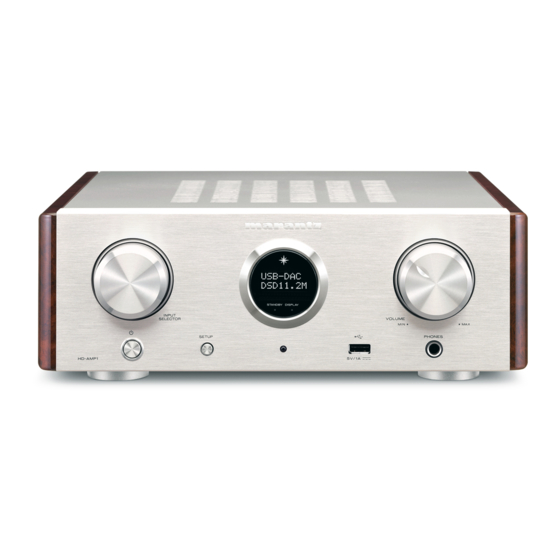
HD-AMP1
Copyright 2016-2018 D&M Holdings Inc. All rights reserved.
WARNING: Violators will be prosecuted to the maximum extent possible.
HD-AMP1 /
U1B/N1B/N1SG
Integrated Amplifier
K1B/FN
Ver. 5
Please refer to the
MODIFICATION NOTICE.
Advertisement
Table of Contents

Related Manuals for Marantz HD-AMP1/U1B/N1B/N1SG


Summary of Contents for Marantz HD-AMP1/U1B/N1B/N1SG
- Page 1 Service HD-AMP1 / U1B/N1B/N1SG K1B/FN Manual Integrated Amplifier • For purposes of improvement, specifications and design are subject to change without notice. • Please use this service manual when referring to the operating instructions without fail. • Some illustrations used in this service manual are slightly different from the actual set. Ver.
-
Page 2: Table Of Contents
Contents ABOUT THIS MANUAL ..............3 TROUBLE SHOOTING ..............34 What you can do with this manual ...........3 1. FLT-DISPLAY doesn't Light ..........34 Using Adobe Reader (Windows version) ........4 2. No Sound. Noise generated ..........35 2.1.1. COMMON (POWER, control signal) ........35 SAFETY PRECAUTIONS ...............6 2.1.2. -
Page 3: About This Manual
ABOUT THIS MANUAL Read the following information before using the service manual. What you can do with this manual Search for a Ref. No. (phrase) Jump to the target of a schematic diagram connector (Ctrl+Shift+F) You can use the search function in Acrobat Reader to search for a Ref. -
Page 4: Using Adobe Reader (Windows Version)
Using Adobe Reader (Windows version) Add notes to this data (Sign) Magnify schematic / printed circuit board The Sign function lets you add notes to the data in diagrams - 1 (Ctrl+Space, mouse operation) this manual. Save the file once you have finished adding notes. Press Ctrl+Space on the keyboard and drag the [Example using Adobe Reader X] mouse to select the area you want to view. - Page 5 Magnify schematic / printed circuit board Magnify schematic / printed circuit board diagrams - 2 diagrams - 3 (Loupe Tool function) (Pan & Zoom function) The Pan & Zoom function lets you see which part of The Loupe Tool function lets you magnify a specific a magnified diagram is being shown in a separate part of a diagram in a separate window.
-
Page 6: Safety Precautions
SAFETY PRECAUTIONS The following items should be checked for continued protection of the customer and the service technician. leakage current check Before returning the set to the customer, be sure to carry out either (1) a leakage current check or (2) a line to chassis resistance check. -
Page 7: Note For Schematic Diagram
NOTE FOR SCHEMATIC DIAGRAM WARNING: Parts indicated by the z mark have critical characteristics. Use ONLY replacement parts recommended by the manufacturer. CAUTION: Before returning the set to the customer, be sure to carry out either (1) a leakage current check or (2) a line to chassis resistance check. If the leakage current exceeds 0.5 milliamps, or if the resistance from chassis to either side of the power cord is less than 460 kohms, the set is defective. - Page 8 Personal notes:...
-
Page 9: Technical Specifications
TECHNICAL SPECIFICATIONS n Audio performance • Rated output 35 W + 35 W(8Ω, 20Hz ~ 20kHz T.H.D. 0.1%) Dynamic power : 70 W + 70 W(4Ω, 20Hz ~ 20kHz T.H.D. 0.1%) Output terminals : Speaker : 4~16Ω (impedance) Compatible with headphones/stereo headphones Playable frequency range : 2 Hz~96 kHz Playable frequency response :... -
Page 10: Dimension
DIMENSION Unit : in. (mm) Weight : 12 lbs 13 oz (5.8 kg) 12 (304) 1 7/8 8 3/8 (210) 1 7/8 (47) (47) -
Page 11: Caution In Servicing
CAUTION IN SERVICING Initializing This Unit Make sure to initialize this unit after replacing the microcomputer or any peripheral equipment, or the PCB. 1. Press the power button to turn off the power. 2. While holding down buttons the " X " and "SETUP" buttons simultaneously, insert the AC plug to turn the power on. 3. -
Page 12: Disassembly
DISASSEMBLY • Remove each part following the flow below. • Reassemble the removed parts in the reverse order. • Read "Precautions During Work" before reassembling the removed parts. • If wire bundles are removed or moved during adjustment or part replacement, reshape the wires after completing the work. - Page 13 Explanatory Photos for DISASSEMBLY • For the shooting direction of each photos used in this manual, see the photo below. A, B, C and D in the photo below indicate the shooting directions of photos. • • The photographs with no shooting direction indicated were taken from the top of the unit. •...
-
Page 14: Side Panel
1. SIDE PANEL Proceeding : SIDE PANEL (1) Remove the screws. ↓Shooting direction: B↓ ↑Shooting direction: A↑ 2. TOP COVER Proceeding : SIDE PANEL → TOP COVER (1) Remove the screws. ↑Shooting direction: D↑ ↑Shooting direction: A↑ ↑Shooting direction: C↑ 3. -
Page 15: Rear Panel
4. REAR PANEL Proceeding : SIDE PANEL → TOP COVER → FRONT ASSY → REAR PANEL (1) Remove the screws. ↓Shooting direction: A↓ (2) Remove the connector. CN71 CN61 5. MAIN PCB Proceeding : SIDE PANEL → TOP COVER → FRONT ASSY → REAR PANEL → MAIN PCB *... -
Page 16: Digital Pcb
7. DIGITAL PCB Proceeding : SIDE PANEL → TOP COVER → FRONT ASSY → REAR PANEL → MAIN PCB → AMP MODULE → DIGITAL PCB (1) Remove the screws. Remove the connector. CN13 CN93 CN21 8. AUDIO PCB Proceeding : SIDE PANEL → TOP COVER → FRONT ASSY → REAR PANEL → MAIN PCB →... -
Page 17: Smps Pcb
9. SMPS PCB Proceeding : SIDE PANEL → TOP COVER → FRONT ASSY → REAR PANEL → MAIN PCB → AMP MODULE → DIGITAL PCB → AUDIO PCB → SMPS PCB (1) Remove the screws. Remove the connector. CUTx3 CN91... -
Page 18: Special Mode
SPECIAL MODE Special mode setting button No. 1 - 4 : While holding down buttons "A" and "B" simultaneously, insert the AC plug into the wall outlet to turn on the power. No. 5 : Press and hold the "B" button for more than 1 second in the Display/LED check mode. Mode Button A Button B Descriptions... -
Page 19: Version Display Mode
1. Version Display Mode Version information is displayed when the device is started in this mode. 1.1. Starting up ·While holding down buttons the " X " and "SETUP" buttons simultaneously, insert the AC plug to turn the power on. ·Next, rotate the "INPUT SELECTOR"... -
Page 20: Display / Led Check Mode
2. Display / LED check mode 2.1. Starting up ·While holding down buttons the " X " and "SETUP" buttons simultaneously, insert the AC plug to turn the power on. ·Next, press the "SETUP" button. 2.2. Actions ·The display and all LEDs light and then go out in a 1 second interval. ·The "INPUT SELECTOR"... -
Page 21: Factory Initialization Mode
4. Factory Initialization Mode Make sure to initialize this unit after replacing the microcomputer or any peripheral equipment, or the PCB. 4.1. Operations ·While holding down buttons the " X " and "SETUP" buttons simultaneously, insert the AC plug to turn the power on. ·Next, press the "SETUP"... -
Page 22: Procedure After Replacing The Printed Circuit Boards
PROCEDURE AFTER REPLACING THE PRINTED CIRCUIT BOARDS. The procedure after replacing the printed circuit boards is as follows. (1) Change the resistor for setting the region. DIGITAL PCB SMPS PCB Model Area R139 R974 R975 R976 North America (U) 120K 120K 120K Europe (N) -
Page 23: Firmware Update Procedure
FIRMWARE UPDATE PROCEDURE 1. USB-A Update (IC22) The latest firmware can be downloaded to a USB memory for updates. 1.1. Connecting to the USB Memory (1) Preparation • Use a memory that supports USB2.0. • USB format : Prepare a USB memory formatted in FAT16 or FAT32. •... - Page 24 1.3. File structure on USB Memory Copy the update files to the USB memory with the following structure. USB memory root + MCS_MLC3730_xxxxxx_Vxx.bin 1.4. Insert the USB memory into the USB port. Download firmware in USB flash drive.
- Page 25 1.5. Operations (1) While holding down buttons the " X " and "SETUP" buttons simultaneously, insert the AC plug to turn the power on. (2) Press "ENTER" on the remote control for more than 5 seconds. (3) The following message appears on the display. Display U S B L o a d i n g...
-
Page 26: Usb-B Update (Ic28)
(3) Move the dedicated driver to the installed folder. (If the installation location of the dedicated driver has not been changed, it is stored in "C:\Program Files\Marantz\Marantz_USB_Driver". ) (4) Rename the binary file for USB update as shown below. ModelName_DFU_MX25L4006E.bin (Ex.) HDAMP1_DFU_MX25L4006E.bin (Do not include a hyphen in the model name.) - Page 27 (3) Move the dedicated driver to the installed folder. ( If the installation location of the dedicated driver has not been changed, it is installed in "C:\Program Files\Marantz\Marantz_USB_Driver" ) (4) Start "MarantzUSBAudioCplApp.exe". (5) Select the "Information" tab, and check that the model name and firmware versions are correct.
-
Page 28: System U-Com Update (Ic11)
3. System u-com Update (IC11) 3.1. Items to Be Prepared (1) Obtain "Flash_loader_demonstrator_vX.X.X_Setup" from the ST Microelectronics website. (2) Personal Computer (Be installed "Flash_Loader_Demonstrator_vX.X.X_Setup.exe"). (3) RS-232C cable (9P (Male), Straight). (4) 8U-210100S WRITING KIT (OLD JIG : SPK-581 WRITING KIT)。 7P FFC (Straight) 3.2. - Page 29 3.3. Installe Flash_Loader_Demonstrator_vX.X.X (1) Run the "Flash_Loader_Demonstrator_vX.X.X_Setup.exe" Click "Yes" (2) Click "Next >". (3) Click Yes".
- Page 30 (4) Enter the user name, company name, and Click "Next". (5) Click "Next". (6) Click "Finish". 3.4. Execute the Flash Loader Demo Run the "STMicroelectronics flash loader.exe" on desktop of PC. (1) Click "Flash Loader Demo".
- Page 31 (2) Select the RS-232C serial port number on your computer. Insert the AC plug of this unit into the power supply. (At this time, the Display of the unit is not lit.) Click "Next" (3) Click "Next". (4) Click "Next".
- Page 32 (5) Checked "Download to device" and click button of "Download from file". Select the file to be updated and click "Open (O)". HD-AMP1_VXXXX.bin (6) Click "Next". HD-AMP1_VXXXX.bin (7) The file is downloaded and written. HD-AMP1_VXXXX.bin...
- Page 33 (8) The following display appears when the firmware update is complete. Click "Close". HD-AMP1_VXXXX.bin (9) Remove the AC plug of this unit from the socket. Remove the 7P FFC form the unit. (10) After updating the firmware, check the version. See "Version Display Mode"...
-
Page 34: Trouble Shooting
TROUBLE SHOOTING 1. FLT-DISPLAY doesn't Light Check Power Supply Voltages for SMPS. N.G. Check the following voltages when this unit is connected to the AC. SMPS PCB [BN93] 11pin / +42V (+42V_VKK) Replace the SMPS PCB. [BN93] 7, 8pin / +5V (+5V_D) [BN93] 5pin / +5V (5V_ST) If these voltages are not output, a fault may have occurred in the SMPS PCB. -
Page 35: No Sound. Noise Generated
2. No Sound. Noise generated 2.1.1. COMMON (POWER, control signal) N.G. Check Power Supply Voltages for USB-A / MLC3730S [IC21]. Check Soldering or replace device / SPMS. DIGITAL PCB SMPS PCB ➡ DIGITAL PCB [IC21] U9, T16, D14, P14, A10, D4, P4pin : +3.3V [BN93] 7, 8pin ➡... - Page 36 N.G. Check Power Supply Voltages for Check Soldering or replace device / SPMS. FLT-DISPLAY / GP1261AI [FL81]. MAIN PCB SMPS PCB ➡ DIGITAL PCB ➡ FRONT CONNECT PCB ➡ FRONT PCB [FL81] 15pin : +42V [BN93] 11pin ➡ [CN93] 11pin : +42V ➡...
-
Page 37: Common (Analog / Digital Sel ➡ Spk Output)
2.1.2. COMMON (ANALOG / DIGITAL SEL ➡ SPK Output) N.G. Check the Audio Signal output and input of ANALOG / DIGITAL Check Soldering or replace device. Selector. MAIN PCB Check the 2.2. ANALOG IN Function : Analog 1 or 2 [RL62] 4pin (ANALOG-Lch), 5pin(ANALOG-Rch) Check the 2.3. - Page 38 Check the operation of the D-AMP module. N.G. Check Soldering or replace device. MAIN PCB MAIN PCB [CN63] 35, 36pin (D-AMP output Lch) [CN63] 17, 18pin (-34V), [CN63] 19, 20pin (+34V) [CN63] 1, 2pin (D-AMP output Rch) [CN63] 9pin (0V) : D-AMP ON ➡ Q661 ➡...
-
Page 39: Subwoofer Out
2.1.3. Subwoofer out N.G. Check Power Supply Voltages for Subwoofer. Check Soldering or replace device. MAIN PCB SMPS PCB ➡ MAIN PCB [IC68] 8pin, [IC67] 8pin : +12V [BN92] 7pin ➡ [CN92] 7pin ➡ [L706] [IC68] 4pin, [IC67] 4pin : -12V [BN92] 4pin ➡... -
Page 40: Analog In
2.2. Analog IN N.G. Check Power Supply Voltages for CD. Check Soldering or replace device. MAIN PCB SMPS PCB ➡ MAIN PCB +12V [BN92] 7pin ➡ [CN92] 7pin : +12V ➡ [L706] -12V [BN92] 4pin ➡ [CN92] 4pin : -12V ➡... -
Page 41: Usb-A / Mlc3730S
2.3. USB-A / MLC3730S Note : The following checks can be performed when the MAIN PCB is removed. (There is no need to use a wire extension jig.) Check Soldering or replace device. Check Power Supply Voltages for OLED. N.G. SMPS PCB ➡... -
Page 42: Usb-B / Xs1U8A128Fb217C10
2.4. USB-B / XS1U8A128FB217C10 Note : The following checks can be performed when the MAIN PCB is removed. (There is no need to use a wire extension jig.) N.G. Check Reset signal for XS1U8A128FB217C10[IC25]. Check Soldering or replace device. DIGITAL PCB DIGITAL PCB [IC25] J2pin : Hi (Lo = Reset) [IC11] 73pin, [R170], [Q205], [Q201]... -
Page 43: Coaxial / Optical 1 / Optical 2
2.5. COAXIAL / OPTICAL 1 / OPTICAL 2 Note : The following checks can be performed when the MAIN PCB is removed. (There is no need to use a wire extension jig.) Check Soldering or replace device. Check the DIR input of S/PDIF signal. N.G. -
Page 44: Measuring Method And Waveforms
MEASURING METHOD AND WAVEFORMS It is recommended to use extension wires between the probe and test points. 1. DIGITAL and MAIN PCB test point • For points q to W3 , take measurements at the points shown in the diagram below. BN71 C659 JK62... - Page 45 Fig.2-1 DSD USB-B out Digital Audio data waveform Fig.2-2 I2S USB-B out Digital Audio data waveform u [IC25] : A9pin i IC25 : A7pin I2S_WFCK/DSD_BCK I2S_SDATA/DSD_L i IC25 : A7pin t [IC25] : A19pin I2S_SDATA/DSD_L USBB_DSD_R y [IC25] : A18pin u [IC25] : A9pin I2S_BCK I2S_WFCK/DSD_BCK...
-
Page 46: Block Diagram
BLOCK DIAGRAM MAIN V/R AUX 1 SPK-RELAY NE5532 AUX 1/2 RELAY DIRECT BYPASS/TONE AUX / DIG HYPEX RELAY ON/OFF RELAY AMP MODULE RELAY SPK-L AUX 2 MUTE SPK-R LINE DET NJM2068 MUTE SUB-W-OUT NJW1163 NJU7181 JITTER REDUCER COAX CS2000 HP-DET NJM2114 /GAIN PROTECTION... -
Page 47: Power Diagram
POWER DIAGRAM HP-AMP1 POWER BLOCK DIAGRAM : Free Voltage SMPS System power consumption 64.49W 174.00W 87.00W SMPS SW UC102 D-AMP 34V 3.00A 87.00W GND A GND_A1 -29V SMPS SW UC102 D-AMP -34V 22.02W 0.02A 0.84W SMPS SW CFLGP1261AI 0.110A 0.243W 0.050A 0.165W ES9010... -
Page 48: Wiring Diagram
WIRING DIAGRAM AC230V~ SPEAKER PCB THERMAL PCB AC INLET CN61 CN71 BN12 BN71 BN61 WF51 CN21 CN91 MAIN PCB CN12 SMPS PCB DAC_H/P PCB DIGITAL PCB CN66 CN32 WF11 WF12 BN85 CN13 TRS1 WF41 BN66 CN81 CN91 BN91 WF62 BN92 BN93 CN82 CN85... -
Page 49: Printed Circuit Boards
PRINTED CIRCUIT BOARDS Lead-free Solder When soldering, use the Lead-free Solder (Sn-Ag-Cu). DIGITAL (A SIDE) DIGITAL (B SIDE) R512 WF13 R511 R505 BK13 R510 R179 R521 R180 L209 C418 R519 C212 JK12 JK13 C417 Q203 R454 R506 IC26 L210 C419 JK14 JK11 JK15... - Page 50 MAIN (A SIDE) MAIN (B SIDE) C689 L616 C690 R482 R481 L608 C686 R414 L701 C692 L603 L601 L607 L702 R620 R797 L602 L606 R801 L604 R798 R802 Q655 R720 Q643 Q632 L611 L605 R698 L704 C670 Q660 R412 R413 R729 R728 Q659...
- Page 51 SPK (A SIDE) SPK (B SIDE) CONNECT_B (A SIDE) CONNECT_B (B SIDE) BK63 JK73 C593 JK72 CN61 C493 CN71 C592 CN65 C492 C604 C601 R500 C605 C602 C591 C491 C606 C603 R400 JK74 JK71 BK64 CN64 SMPS (A SIDE) SMPS (B SIDE) Q933 DB91 CUP12809Z-A...
-
Page 52: Schematic Diagrams (01/08)
CN12 TO 6B TO BN12 CN12 TO 5B CJP03GA208ZY Rear Pannel(for Update) WF11 WF11 3.3V_D1 CJP19GA291ZN MCU+3V3 R174 100K MCU+3V3 R173 PDAT FL_DA WF13 PCLK FL_CLK CJP07GB310ZY PCEN FL_CS MCU+3V3 R182 FPRS FL_RST OPEN R183 KEY2 Q131 KEY2 Q102 L108 CLZBLM21PG221SN1 Q103 HVTKRC102S... -
Page 53: Sch02_Digital_2
VDD33IO USBA_VBUS CN21 C212 0.1uF CN21 IC22 TO B2 CVIMX25L1606EM2I-12G CJP05GA208ZY C213 100/16V +5V_VBUS SF_CS -DATA USB_DM R291 5.1K +DATA SF_DO USB_DP HOLD# L201 CLZBLM21PG221SN1 R289 SCLK SF_CLK SHIELD L202 TO CN83 CLZBLM21PG221SN1 SF_DI VDD33IO VDD33IO C256 16V/22uF R288 VDD33IO VDD33IO C255 0.1uF... -
Page 54: Sch03_Digital_3
C339 L305 3.3V_D1 CLZBLM21PG221SN1 16V/22uF R335 TO D0 C338 TO C8 0.1uF +5V_D TO C1 D301 +3.3D1_2 +3.3V_DA_2 CVD1SS355T IC43 CLK_24M/22M_SEL CVIADUM1285CRZ Q301 R315 HVTKRA102S D302 VDD1 VDD2 TO A0 CVD1SS355T R344 R337 Q302 RC5F HVTKRC102S JK11 CJJ4N076Z R345 3.3V_A RC5S GND1 GND2... -
Page 55: Sch04_Main
+12V_A Q506 CVTKSC1845FTA AGND Q505 CVTKSA992FTA R503 GAIN 4.7K Q530 HVTKTC2875B Q504 3.3V_A CVTKSA992FTA BN66 R516 R517 R520 BN66 1.8K 3.3K AGND Q503 CWB13 CVTKSC1845FTA R518 R478 CVTKSC1845FTA +12V +12V_A Q507 HD_DET L506 PG221SN OPEN AGND AGND AGND CVTKSC1845FTA Q502 AGND AGND AGND... -
Page 56: Sch05_Audio
SPK-DC- PROTECTION CJJ4M073ZY C426 0.1uF R689 L601 JK61 CLZBLM21PG221SN1 C427 0.01uF C428 1000pF R690 SPK_DC_PRO CHGND AGND R691 Q582 C429 0.1uF C480 0.1uF HVTKRA107S +12V R419 C430 0.01uF C481 0.01uF RL61 AUX1 R692 RL+12V CVTKSC1845FTA CSL4A015ZU C431 1000pF C482 1000pF AGND AGND CHGND Q581... -
Page 57: Sch06_Front
WF81 TO WF11 WF81 CJP19GB116ZY BK85 WF82 CMD1A569-V1 GND1 WF82 CJP19GI281Z TO WF83 FROM DIGITAL_BD FROM DIGITAL_BD WF83 TO WF82 CJP19HJ282Z WF83 TO CN21 CN83 to POWER CN83 CN84 CJP05GA19ZY CJP04GA19ZY to MAIN (DIGITAL) F+3.3V F+3.3V RC81 GNDF2 F+3.3V IC81 Q801 CVINJM2887DL3 KRA102S... -
Page 58: Sch07_Smps
HD-AMP1 SMPS SCHEMATIC DIAGRAM AC-L C922 L921 TF93 1KV 471 J CLZ9R001Z L924 BN91 +29V_AMP BN91 D925 BD91 R912 C936 +29V_AMP FCU20A40 50V 1000uF +29V_AMP (400V/20A) 1KV 102 K +29V_AMP +29V_AMP BD92 DGND C935 DGND 100MHz_60ohm_6A 100MHz_60ohm_6A DGND 50V 1000uF L926 -29V_AMP TO CN91... -
Page 59: Sch08_Connct
SPK TERMINAL BD JK71 JK72 JK73 JK74 C493 C593 0.1uF 0.1uF 1000pF/100V 1000pF/100V C492 C592 3R3-F 3R3-F 0.01uF 0.01uF R400 C491 C591 R500 CN61 CN71 CN61 CN71 CJP02GA89ZY CJP02GA89ZY TO BN61 TO BN71 D-AMP-CONNECTOR BD CN65 CJP36GA221ZB C601 C604 0.1uF 0.1uF C602 C605... -
Page 60: Exploded View
EXPLODED VIEW Please see the last chapter for the part list. S2 x3 S2 x3 C6 -1 C3 -6 S1 X4 S2 x8 S1 x9 M19 X4 S5 x4 C4 -1 NUTX4 S4 x2 S2 x2 C4 -2 C4 -6 S5 x2 C4 -7 S2 x2... -
Page 61: Packing View
PACKING VIEW Please see the last chapter for the part list. ADHSIVE 20 2 (C4FA101) 20 3 20 4 20 2 20 5 MANUFACTURE DATE LABEL Replace to UK plug (UK version only) -
Page 62: Semiconductors
SEMICONDUCTORS Only major semiconductors are shown, general semiconductors etc. are omitted to list. The semiconductor which described a detailed drawing in a schematic diagram are omitted to list. 1. IC's UcD102OEM (D-AMP) CVISTM32F101ZE (DIGITAL : IC11) PIN Functions ポート名 Function PD/PU STBY DESCRIPTION V_PROTECT... - Page 63 ポート名 Function PD/PU STBY DESCRIPTION VSS_5 GND FIX VDD_5 3.3V PF10 PH0 / OSC_IN XTAL_IN 8Mhz Xtal PH1 / OSD_OUT XTAL_OUT 8Mhz Xtal NRST RESET RESET KEY1 KEY PORT KEY2 KEY PORT VOL_DOWN MOTOR VR DOWN MODEL_ID1 OPTION PORT VSSA GND FIX VREF- GND FIX...
- Page 64 ポート名 Function PD/PU STBY DESCRIPTION PD13 VSS_8 GND FIX VDD_8 3.3V PD14 BYPASS/TONE1_SEL BYPASS/TONE1_CNT PD15 BYPASS/TONE2_SEL BYPASS/TONE2_CNT SPK_RL_CNT SPK RELAY Control AMP_ON/OFF AMP_ON/OFF DC_ERROR_DET No use P_CONT SMPS POWER CTL USBB_MCLK_SEL USB-B MCLK SELECT VSS_9 GND FIX VDD_9 3.3V THERMAL DET THERMAL PROTECT DETECT AMP_VCC_DET DC_PROTECT2 DETECT...
- Page 65 ■ 長 外形寸法図 (単位:mm) PQ033DNA1ZPH (DIGITAL : IC10, IC17) 電流:1A ±0.5 MAX. 圧 Vin(MAX)=24V ±0.5 (0.3) 費電流 荷時消費電流:MAX.8mA エポキシ樹脂 0 5 0 D N A 1 時消費電流:MAX.5μA) 端子処理識別マーク OFF機能内蔵 流保護、過熱保護機能内蔵 (0~0.25) 保護機能内蔵 +0.2 (0.3) ミックコンデンサ対応 -0.1 4-(1.27) S指令対応品 ・( )内はTYP.値 途 製品質量:(0.2g) 機器...
- Page 66 ■ PST83XX, PST84XX 端子接続図 ■ PST83XX, PST84XX PST8425NR (DIGITAL : IC13) Vref 静電保護素子 SOT-25A SSON-4 (TOP VIEW) (TOP VIEW) SOT-25A SSON-4 ■ PST84XX (回路図中の①~④はSSON-4パッケージのピン番号です。 ) (TOP VIEW) (TOP VIEW) Block diagram SC-82AB (TOP VIEW) SC-82AB Vref (TOP VIEW) 端子説明 静電保護素子 ■...
- Page 67 Internal Thermal Overload Protection Bipolar Technology Package Outline TO-252-3 (NJM2845DL1), TO-252-5 (NJM2846DL3) NJM2845DL133 (DIGITAL : IC15) PIN CONFIGURATION 1.CONTROL 2.GND 3.GND 4.Vo ピン配置図 5.NC 1 2 3 4 5 SOT-223 TO-263 LM1117-N (DIGITAL : IC16, IC18 MAIN : IC53) NJM2845DL1 NJM2846DL3 EQUIVALENT CIRCUIT ブロ...
- Page 68 MLC3730 (DIGITAL : IC21) MLC3730 0x PIN Functions 1.3.2 MLC3730S MLC373 0M6, MLC3 3730M1 ‐BGA) N ESCRIPTION PAD Type Description n PAD Ty escription O Output PAD POWER Digital Power 3.3V o or 1.2V ISPU Input PAD Sc chmitt trigger with Pull Up Digital IO or Interna al Ground ...
- Page 69 MLC3730 0x 33‐M2 PGPB13 BS HU2‐RD ECSN DIO3‐D3 PAD19 34‐M1 PGPB14 BS EMCLK‐ ‐0 UCLK AND‐CLE 35‐N1 PGPB15 BS ELRCK SDIO O1‐D4/ AND‐ALE SDIO O1‐D2OE 36‐N4 PGPC00 BS EBCLK SDIO O1‐D1 AND‐REB 37‐N2 PGPC01 BS SDIO O1‐D2 AND‐WEB ...
- Page 70 MLC3730 0x 127‐D16 PD[11] B Externa al Bank, SDRA M, NAND Flas sh data bus [1 11] input/outp 128‐C16 PD[12] B Externa al Bank, SDRA M, NAND Flas sh data bus [1 12] input/outp 129‐C17 PD[13] B Externa al Bank, SDRA M, NAND Flas sh data bus [1 13] input/outp 130‐B17 PD[14] B Externa al Bank, SDRA M, NAND Flas sh data bus [1 14] input/outp 131‐E13 VSS33IO GND ...
- Page 71 MX25L1606E (DIGITAL : IC22) SO/SIO1 HOLD# W P# SCLK SI/SIO0 PIN Functions W9864G6JH (DIGITAL : IC23) PIN Functions PIN NUMBER PIN NAME FUNCTION DESCRIPTION Multiplexed pins for row and column address. Row address: A0- A11. Column address: A0- A7. 23 ~ 26, 22, Address A0- A11 29 ~35...
- Page 72 XS1-U8A-128-FB217 (DIGITAL : IC25) X1D05 X1D06 X1D07 X1D08 X1D09 X1D10 X1D11 X1D12 X1D13 X1D14 X1D15 X1D16 X1D17 X1D18 X1D19 X1D20 X1D21 X1D22 X1D23 X1D04 X1D53 X1D54 X1D55 X1D56 X1D57 X1D58 X1D61 X1D62 X1D63 X1D64 X1D65 X1D66 X1D67 X1D68 X1D69 X1D70 X1D24 X1D25 X1D03...
- Page 73 Module Name Function Type Active Properties X0D14 — P16A P32A X0D15 — P16A P32A X0D16 — P16A X0D17 — P16A X0D18 — P16A X0D19 — P16A X0D20 — P16A P32A X0D21 — P16A P32A X0D22 — X0D24 — X0D35 — X0D43/WAKE —...
- Page 74 TC7SH125FU (DIGITAL : IC26) PIN Functions MX25L4006EM2I-12G (DIGITAL : IC28) PIN CONFIGURATIONS PIN DESCRIPTION SYMBOL DESCRIPTION 8-PIN SOP (150/200mil) 8-PIN PDIP (300mil) Chip Select Serial Data Input (for 1 x I/O) / Serial Data HOLD# SI/SIO0 SO/SIO1 SO/SIO1 HOLD# Input & Output (for Dual Output mode) SCLK SCLK SI/SIO0...
- Page 75 PCM9211PTR (DIGITAL : IC31) Block Diagram Pin Discriptions...
- Page 76 ADuM1285 (DIGITAL : IC43,44,45,46) EMP8020-13VF05NRR (MAIN : IC51) EMP8020-XXVF05NRR Output voltage VF05 SOT-23-5 Package NRR RoHS & Halogen free package Rating: -40 to 85°C Package in Tape & Reel PIN Functions Name SOT-23-5 Function VOUT Output Voltage Feedback Supply Voltage Input Require a minimum input capacitor around 1µF to ensure stability and sufficient decoupling from the ground pin.
- Page 77 ES9010K2M (MAIN : IC52) DGND ES9010K2M 28-QFN XI ( PIN Functions PIN DESCRIPTIONS Reset Name Pin Type Pin Description State DGND Ground Ground Digital Ground N.C. No internal connection. Pin may be grounded if desired. Tri-stated C Serial Clock Input Tri-stated C Serial Data Input/Output ADDR...
- Page 78 NJU7181_E (MAIN : IC62) MSOP8 (TVSP8) Symbol Function NJW1163_E (MAIN : IC66)
- Page 79 NJM2887_E (FRONT : IC81) FDC608PZ (DIGITAL : Q203) SuperSOT -6 Absolute Maximum Ratings C unless otherwise noted – Gate-Source Voltage ±12 Drain Current – Continuous –5.8 (Note 1a) – – Maximum Power Dissipation (Note 1a) (Note 1b) Operating and Storage Junction Temperature Range –55 to +150 °C Thermal Characteristics...
-
Page 80: Display
2. DISPLAY FLD (GP1261AI) (FL81) DIMENSION PIN CONNECTION PTTERN DETAIL... - Page 81 MAIN MAIN PCB ASS'Y ※Parts indicated by "nsp"on this table cannot be supplied. ※The parts listed below are only for maintenance. Therefore they might differ from the parts used in the unit in appearances or dimensions NOTE:The symbols in the column Remarks indicate the following destinations. U : North America model N : Europe model K : China model F : Japan model BK : Black model SG : Silver Gold model...
- Page 82 MAIN REF No. Part No. Part Name Remarks Q'ty New Ver Q706 943213500150S NPN, TO-92, LOW NOISE, HFE:300-600, FAILCHILD CVTKSC1845FTA Q707,708 00D9430072502 T.R , CHIP , SOT-23 HVTKTC2875B Q709 00D2690192902 T.R , CHIP , SOT-23 HVTKRC102S Q710 00D2690184907 T.R , CHIP , SOT-23 HVTKRA102S Q711 00D9430072502...
- Page 83 MAIN REF No. Part No. Part Name Remarks Q'ty New Ver R559 RES, CARBON(1/5W,68ohm,J) CRD20TJ680T R560 RES, CARBON(1/5W,5.6Kohm,J) CRD20TJ562T R561 RES, CARBON(1/5W,22Kohm,J) CRD20TJ223T R562 RES, CARBON(1/5W,100ohm,J) CRD20TJ101T R563,564 RES, CARBON(1/5W,47ohm,J) CRD20TJ470T R565 RES, CARBON(1/5W,5.6Kohm,J) CRD20TJ562T R566 RES, CARBON(1/5W,1.8Kohm,J) CRD20TJ182T R567 RES, CARBON(1/5W,10Kohm,J) CRD20TJ103T R569...
- Page 84 MAIN REF No. Part No. Part Name Remarks Q'ty New Ver R702,703 RES, CHIP(1608/5%/1Kohm) CRJ10DJ102T R704 RES, CARBON(1/5W,47ohm,J) CRD20TJ470T R705 RES, CARBON(1/5W,100Kohm,J) CRD20TJ104T R706 00MGG0510016X RES , CFPS1/4CMHTA100J CRG14SANJ100CLP R707 RES, CARBON(1/5W,10ohm,J) CRD20TJ100T R708 RES, CARBON(1/5W,15Kohm,J) CRD20TJ153T R709 RES, CARBON(1/5W,1Kohm,J) CRD20TJ102T R710 RES, CARBON(1/5W,15Kohm,J)
- Page 85 MAIN REF No. Part No. Part Name Remarks Q'ty New Ver C436 CAP, CHIP(1608, 50V/0.01uF, X7R)_SAMSUNG CCUS1H103KCS C437 CAP, CHIP(1608, 50V/1000pF, X7R)_SAMSUNG CCUS1H102KCS C438 CAP, CHIP(1608, 50V/0.1uF, X7R)_SAMSUNG CCUS1H104KCS C439 CAP, CHIP(1608, 50V/0.01uF, X7R)_SAMSUNG CCUS1H103KCS C440 CAP, CHIP(1608, 50V/1000pF, X7R)_SAMSUNG CCUS1H102KCS C451 CAP, CHIP(1608, 50V/0.01uF, X7R)_SAMSUNG...
- Page 86 MAIN REF No. Part No. Part Name Remarks Q'ty New Ver C680 943133501450D CAP , FNS (135)-100VDC-222J CCMP2A222JS13T C681 CAP, MYLAR(50V/0.033uF/J) HCQI1H333JZT C682 943133502600S CAP, POLYPROPTLENE(FNS(135)-100VDC-223K) CCMP2A223JS13T C683 CAP, MYLAR(50V/0.047uF/J) HCQI1H473JZT C684 CAP , MYLAR(63V/0.47uF/J) CCQI1W474JZT C685 CAP, CHIP(1608, 50V/0.1uF, X7R)_SAMSUNG CCUS1H104KCS C686 CAP, CHIP(1608, 50V/1000pF, X7R)_SAMSUNG...
- Page 87 DIGITAL DIGITAL PCB ASS'Y ※Parts indicated by "nsp"on this table cannot be supplied. ※The parts listed below are only for maintenance. Therefore they might differ from the parts used in the unit in appearances or dimensions NOTE:The symbols in the column Remarks indicate the following destinations. U : North America model N : Europe model K : China model F : Japan model BK : Black model SG : Silver Gold model...
- Page 88 DIGITAL REF No. Part No. Part Name Remarks Q'ty New Ver R154,155 RES, CHIP(1608/5%/0ohm) CRJ10DJ0R0T R156,157 RES, CHIP(1608/5%/56ohm) CRJ10DJ560T R158,159 RES, CHIP(1608/5%/0ohm) CRJ10DJ0R0T R160 RES, CHIP(1608/5%/10Kohm) CRJ10DJ103T R161 RES, CHIP(1608/5%/100Kohm) CRJ10DJ104T R162-164 RES, CHIP(1608/5%/56ohm) CRJ10DJ560T R165,166 RES, CHIP(1608/5%/0ohm) CRJ10DJ0R0T R167,168 RES, CHIP(1608/5%/10Kohm) CRJ10DJ103T R170-172...
- Page 89 DIGITAL REF No. Part No. Part Name Remarks Q'ty New Ver R413 RES, CHIP(1608/5%/10Kohm) CRJ10DJ103T R414 RES, CHIP(1608/5%/51ohm) CRJ10DJ510T R415 RES, CHIP(1608/5%/22ohm) CRJ10DJ220T R416 RES, CHIP(1608/5%/0ohm) CRJ10DJ0R0T R417 RES, CHIP(1608/5%/51ohm) CRJ10DJ510T R420 RES, CHIP(1608/5%/10Kohm) CRJ10DJ103T R421 RES, CHIP(1608/5%/51ohm) CRJ10DJ510T R426,427 RES, CHIP(1005/5%/10Kohm) CRJ06IJ103T R428,429...
- Page 90 DIGITAL REF No. Part No. Part Name Remarks Q'ty New Ver C236 CAP, CHIP(1005, 16V/0.1uF, X7R)_SAMSUNG CCUI1C104KCS C237 CAP, CHIP(1005, 25V/0.01uF, X7R)_SAMSUNG CCUI1E103KCS C238 CAP, CHIP(1005, 16V/0.1uF, X7R)_SAMSUNG CCUI1C104KCS C239 CAP, CHIP(1005, 25V/0.01uF, X7R)_SAMSUNG CCUI1E103KCS C240 CAP, CHIP(1005, 16V/0.1uF, X7R)_SAMSUNG CCUI1C104KCS C241 CAP, CHIP(1005, 25V/0.01uF, X7R)_SAMSUNG...
- Page 91 DIGITAL REF No. Part No. Part Name Remarks Q'ty New Ver JK14 943643103370S JACK,RCA (1P,BK, GOLD , GND PLATE) CJJ4M094Z JK15 943643102880S JACK , USB_B TYPE CJJ9L020Z L101-113 FERRITE CHIP BEAD(2012/220R) CLZBLM21PG221SN 13 L115 FERRITE CHIP BEAD(2012/220R) CLZBLM21PG221SN 1 L201-211 FERRITE CHIP BEAD(2012/220R) CLZBLM21PG221SN 11 L212,213...
- Page 92 SMPS SMPS PCB ASS'Y ※Parts indicated by "nsp"on this table cannot be supplied. ※The parts listed below are only for maintenance. Therefore they might differ from the parts used in the unit in appearances or dimensions NOTE:The symbols in the column Remarks indicate the following destinations. U : North America model N : Europe model K : China model F : Japan model BK : Black model SG : Silver Gold model...
- Page 93 SMPS REF No. Part No. Part Name Remarks Q'ty New Ver R944 RES, CHIP(2012/5%/33ohm) CRJ18AJ330T R945 RES, CHIP(2012/5%/1.8Kohm) CRJ18AJ182T R946 RES, CHIP(2012/1%/3.9Kohm) CRJ18AF3901T R947 RES, CHIP(2012/1%/120Kohm) CRJ18AF1203T R948 RES, CHIP(2012/5%/0ohm) CRJ18AJ0R0T R949 RES, CHIP(2012/5%/18Kohm) CRJ18AJ183T R950 RES, CHIP(2012/5%/1.8Kohm) CRJ18AJ182T R951 RES, CHIP(2012/5%/2.2Kohm) CRJ18AJ222T R952...
- Page 94 SMPS REF No. Part No. Part Name Remarks Q'ty New Ver BN91 WIRE ASS'Y(7P,300mm,2.5mm) CWB1D00730058 BN92 WIRE ASS'Y(7P,180mm,2.0mm) CWB1C00718047 BN93 WIRE ASS'Y(11P,250mm,2.0mm) CWB1C011250AA7 CN61 WAFER, 2P, 7.92mm CJP02GA89ZY CN64,65 2.54mm 36PIN WAFER CJP36GA349ZP CN71 WAFER, 2P, 7.92mm CJP02GA89ZY CN91 WAFER, 2P, 3.96mm CJP02KA060ZY ! CX91,92 943132100570S...
- Page 95 FRONT FRONT PCB ASS'Y ※Parts indicated by "nsp"on this table cannot be supplied. ※The parts listed below are only for maintenance. Therefore they might differ from the parts used in the unit in appearances or dimensions NOTE:The symbols in the column Remarks indicate the following destinations. U : North America model N : Europe model K : China model F : Japan model BK : Black model SG : Silver Gold model...
- Page 96 FRONT REF No. Part No. Part Name Remarks Q'ty New Ver ★ BRACKET , PCB CMD1A629 ★ IR BRACKET CMD1A944...
- Page 97 EXPLODED EXPLODED ※Parts indicated by "nsp"on this table cannot be supplied. ※The parts listed below are only for maintenance. Therefore they might differ from the parts used in the unit in appearances or dimensions. NOTE:The symbols in the column Remarks indicate the following destinations. U : North America model N : Europe model K : China model F : Japan model BK : Black model SG : Silver Gold model...
- Page 98 EXPLODED REF No. Part No. Part Name Remarks Q'ty New Ver 943606502930S CARD CABLE (17P 1.25MM 60MM) CWC4C4A17B060B08 SCREW GROUP SCREW CTB3+10JFB SCREW CTB3+8JFB SCREW CTWS3+10GR SCREW CTS3+8JFB SCREW CHD2A060R SCREW CTB3+6FFB SCREW CTW3+6JR SCREW CTB3+6JFB SCREW CTW3+8JFB...
- Page 99 PACKING PACKING ※Parts indicated by "nsp"on this table cannot be supplied. ※The parts listed below are only for maintenance. Therefore they might differ from the parts used in the unit in appearances or dimensions. NOTE:The symbols in the column Remarks indicate the following destinations. U : North America model N : Europe model K : China model F : Japan model BK : Black model SG : Silver Gold model...
Need help?
Do you have a question about the HD-AMP1/U1B/N1B/N1SG and is the answer not in the manual?
Questions and answers
Esquema som lg modelo ck43