Table of Contents
Advertisement
Advertisement
Table of Contents

Related Manuals for SEPTENTRIO mosaic Series


Summary of Contents for SEPTENTRIO mosaic Series
- Page 1 Mosaic Hardware Manual Version 1.7.0...
- Page 2 Hardware Manual Version 1.7.0 September 7, 2022 © Copyright 2000-2022 Septentrio nv/sa. All rights reserved. Septentrio Greenhill Campus, Interleuvenlaan 15i 3001 Leuven, Belgium http://www.septentrio.com Phone: +32 16 300 800 Fax: +32 16 221 640 @septentrio...
-
Page 3: Table Of Contents
1 Table of contents TABLE OF CONTENTS ....................3 DOCUMENT CHANGE LOG ..................7 MOSAIC GNSS MODULE ....................8 Overview ........................8 Mechanical ......................10 Absolute Maximum Ratings ................. 10 Electrical Characteristics in Operational Conditions ........11 3.4.1 Power Supply ......................11 3.4.2 I/O .......................... - Page 4 Event/TimeSync inputs ..................23 PPS output ......................24 4.10 General Purpose Output (GPx) ................24 4.11 LEDs ......................... 25 4.12 Standby ........................25 4.13 RTC ........................... 27 MOSAIC INTEGRATION ....................28 Minimal Design ...................... 28 5.1.1 Single-Antenna Modules ..................29 5.1.2 Dual-Antenna Modules ..................
- Page 5 Header Types ......................40 Powering the DevKit ..................... 40 Antenna Connectors ..................... 41 LEDs and General Purpose Output Pins ............. 42 COM Ports ....................... 43 PPS Out and Event Inputs ..................44 Ethernet ........................44 USB Dev ........................44 USB Host ......................... 44 7.10 REF IN ........................
- Page 6 APPENDIX E PAD LIST ....................57...
-
Page 7: Document Change Log
Document Change Log 2 Document Change Log Document Release Main Changes Release Date 1.1.0 Oct 2019 First published version 1.2.0 Jun 2020 Extended the description of the standby mode Added description of the MODULE_RDY pin Added power state diagram Extended and clarified the “Product Handling” section 1.3.0 Jul 2020 Added a note that the RTC_XTALI pin must be tied to ground... -
Page 8: Mosaic Gnss Module
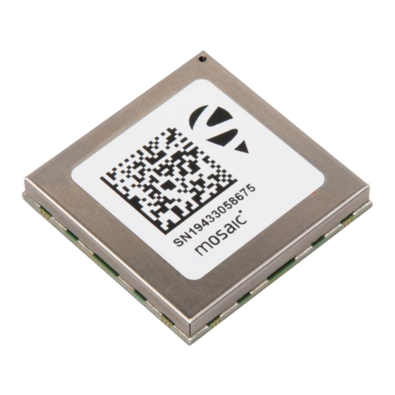
GNSS Module 3 mosaic GNSS Module 3.1 Overview Septentrio’s mosaic modules are low-power multi-band multi-constellation GNSS receiver packaged in a 31x31mm LGA module. The internal block diagram is shown below. The module operates from a single 3V3 power supply (VDD_3V3). - Page 9 mosaic GNSS Module Ethernet (the PHY is external to the module). See section 4.5. • SDCard interface for logging to an external SD card. See section 4.6. • GPIO and LEDs output. See section 4.10. • The table below summarizes the main differences between the mosaic models in terms of hardware features.
-
Page 10: Mechanical
mosaic GNSS Module 3.2 Mechanical All dimensions in millimeters. Weight = 6.8g LGA Details Specification Land pitch 1.27 mm Land diameter 0.6 mm Pin 1 mark Bottom: the A1 pad is missing Top: A1 marked by the hole in the shield Land plating Nickle/Gold Array... -
Page 11: Electrical Characteristics In Operational Conditions
mosaic GNSS Module EVENT input voltage See 4.8 -0.3 1V8_OUT+0.3 RF input power at ANT_1 See 4.2 RF input power at ANT_2 See 4.2 REF_I level See 4.7 Vp-p Output pins drive current Storage temperature °C Operational temperature °C 3.4 Electrical Characteristics in Operational Conditions 3.4.1 Power Supply Parameter Comment... -
Page 12: Power Consumption
mosaic GNSS Module 3.5 Power Consumption The module is powered through the VDD_3V3 pins, see section 4.1. The power consumption depends on the set of GNSS signals enabled and on the positioning mode. The following tables list the average power consumption for some configurations, while tracking all satellites in view from an open sky, and with the module at room temperature. -
Page 13: Pinout And I/O Description
Pinout and I/O Description 4 Pinout and I/O Description The module provides 239 LGA pads, configured as follows. The following sections describe all the non-reserved pads. Pads are grouped by functions. A complete pad list can be found in Appendix E. Conventions: Pin Type: I=Input, O=Output, P=Power, Ctrl=Control, Clk=Reference clock •... -
Page 14: Power Supply
Pinout and I/O Description 4.1 Power Supply The module is powered through the VDD_3V3 pins. Pin Name Type Level Description Comment VDD_3V3 3.3V +/-5% Main power supply input All VDD_3V3 pins must be tied together. Ground All GND pins must be connected to ground. -
Page 15: Auxiliary Antenna
Pinout and I/O Description 4.2.1.1 ANT_1 Electrical Specifications DC bias DC level provided with the VANT pad Equivalent DC series impedance at 2.5 Ohms typical, 3.0 Ohms max the ANT_1 pin Antenna current limit 150 mA ANT_1 pre-amplification gain range Single-antenna modules: 15-50 dB (AGC gain: 15-50dB) Dual-antenna modules: 15-35dB (AGC gain: 30-50dB) ANT_1 receiver noise figure... -
Page 16: Typical Application
Pinout and I/O Description 4.2.3 Typical Application 4.2.3.1 Single Antenna Modules The ANT_1 input is DC-biased and ESD-protected, so that no external component is needed. Make sure to connect the ANT_2 pad to ground. Refer to 5.5.3 for RF-routing recommendations. 4.2.3.2 Dual-Antenna Modules The main antenna connects to ANT_1 and the auxiliary antenna to ANT_2. -
Page 17: Com Ports
Pinout and I/O Description 4.3 COM Ports The module provides four serial COM ports. Three of them (COM1 to COM3) support RTS/CTS hardware flow control: Pin Name Type Level Description Comment TXD1 3V3_LVTTL Serial COM1 transmit line (inactive state is high) RXD1 I, PU 3V3_LVTTL... -
Page 18: Usb Device Interface
Pinout and I/O Description 4.4 USB Device Interface The following pins are used for accessing the module over USB in USB-device mode. Pin Name Type Level Description Comment USB_VBUS1 4.40V to USB VBUS input. This pin powers the integrated PHY of 5.5V the USB interface. -
Page 19: Ethernet
Pinout and I/O Description 4.5 Ethernet The module supports full duplex 10/100 Base-T Ethernet communication. The Ethernet PHY and magnetics are to be implemented on the host board. Connection with the PHY is through the RMII interface available on the following pins: Pin Name Type Level... -
Page 20: Sd Memory Card
PHY output pins are not driven when the module is not powered. The module also supports other PHYs. An up-to-date list of supported PHY’s can be found in Septentrio’s Knowledge Base pages : https://customersupport.septentrio.com/s/article/which-ethernet-phy-does-mosaic-support 4.6 SD Memory Card The module can interface to an external SD memory card through the pins listed in the table below. -
Page 21: Typical Application
Pinout and I/O Description 4.6.1 Typical Application The module supports the 1-bit SD transfer mode with 3V3 signaling. An example circuit to a 9-pin SD memory card socket is shown below. The maximum clock frequency (SD_CLK) is 33.000 MHz. 4.6.2 Data Logging Driving the LOGBUTTON pin low for 100 ms to 5 seconds toggles logging on and off. -
Page 22: Clock Frequency Reference
Pinout and I/O Description 4.7 Clock Frequency Reference The module can use its internal TCXO frequency reference, or can accept an external frequency reference, bypassing the internal TCXO. Pin Name Type Level Description Comment REF_I 0.5-1.7Vp-p Main frequency reference input, DC-decoupled, input capacitance See section 4.7.2. -
Page 23: Event/Timesync Inputs
Pinout and I/O Description sufficiently low to avoid excessive level drop because of the filtering of the divider with the input capacitance of the REF_I input (8 pF). Below an example circuit. The module has a build-in DC-decoupling capacitor. Support for an external frequency reference is not available in all mosaic models. It is only available on those models where the FreqSync permission is enabled. -
Page 24: Pps Output
Pinout and I/O Description Note the timing signals use 1.8V logic. If 3.3V logic would be required, the EVENT-signals can be generated via a resistive divider, considering the integrated pull-down (see 3.4.2). They could as well be created via a level shifter, using the 1V8_OUT output from the module to supply the module side. -
Page 25: Leds
Pinout and I/O Description During the first seconds after powering up the module, these pins are in tristate. Use an external pull-down or pull-up resistor to have the desired level during boot. The GPx pins can drive a maximum current of 10mA. 4.11 LEDs The LED pins can be used to monitor the module status. - Page 26 Pinout and I/O Description PMIC_ON_REQ 3V3_LVTTL Typically connected to the control pin of an external power switch. The power switch is expected to enable VDD_3V3 when PMIC_ON_REQ is high, and to disable VDD_3V3 when it is low. MODULE_RDY 3V3_LVTTL Level is high when module is operating, and low when in standby Level becomes high...
-
Page 27: Rtc
Pinout and I/O Description Note that the ONOFF pin can also be used without external power switch (i.e. when VDD_3V3 is tied to VDD_BAT). The module will then stop all software and unmount the external SD card, but will not enter low power consumption. It will automatically wake up again after about 2 minutes. -
Page 28: Mosaic Integration
mosaic Integration 5 mosaic Integration Minimal Design A minimal design for single-antenna and dual-antenna modules is shown below. In both cases: All ground pins and the pins marked “Reserved_GND” are connected to ground • (GND). A 3.3VDC supply is provided to the VDD_3V3 pins and to the VDD_BAT pin. A 22µF •... -
Page 29: Single-Antenna Modules
mosaic Integration 5.1.1 Single-Antenna Modules In single antenna mosaic modules, the ANT_2 pin (V23) must be tied to ground. -
Page 30: Dual-Antenna Modules
mosaic Integration 5.1.2 Dual-Antenna Modules The main antenna connects to ANT_1 (AC20) and the auxiliary antenna connects to ANT_2 (V23). DC supply is provided through the ANT_1 pin, and the biasing circuit to supply the auxiliary antenna is shown (see also section 4.2.3.2). Inductor self resonant near 1400MHz, e.g. -
Page 31: Decoupling
mosaic Integration Many pins are reserved, which means that their functionality is proprietary or is • not supported yet by the firmware. Reserved pins are marked “Reserved_NC” and “Reserved_GND”. The Reserved_NC pins must be left unconnected. Reserved_GND pin (i.e. only AB7) must be tied to ground. 5.3 Decoupling The VDD_3V3 supply shall be decoupled with at least a 22 µF capacitor with proper voltage rating. -
Page 32: Layout Recommendations
mosaic Integration 5.5 Layout Recommendations 5.5.1 Coplanarity It is important to avoid warpage of the motherboard on which the module will be soldered. More in particular: Use a symmetrical layer stack • Make sure layers opposite from the center of the board have a similar amount of •... -
Page 33: Avoiding Self-Interference
mosaic Integration 5.5.4 Avoiding Self-Interference Antenna input connections are sensitive to interference from higher harmonics of other signals on the board. Even clock signals of just a few MHz can produce harmful harmonics at GNSS frequencies (1155-1300 MHz and 1540-1610 MHz). It is best to keep antenna input traces short, to reduce the area in which signals can be picked up. -
Page 34: Product Handling
The mosaic module should be stored and handled in the original package (preferably) or in a conductive foam shorting all pads. 6.2 ROHS/WEEE NOTICE Septentrio receivers and modules are compliant with the latest WEEE, RoHS and REACH directives. For more info see www.septentrio.com/en/environmental-compliance. -
Page 35: Packaging
Product Handling 6.3 Packaging Mosaic modules are delivered on a tray in a dry pack, with 27 modules per tray. Package contents: 27 mosaic modules • 1 humidity indicator • 1 desiccator bag • Packing list Label • Process lot label •... -
Page 36: Packing List Label
6.3.1 Packing List Label The labeling gives product information: Product: mosaic variant with hardware revision • Quantity: number of modules in the bag • PN: Septentrio Part Number • MPN: Manufacurer Part Number • MPL: Manufacturer Product Lot • Date: Packaging Date •... -
Page 37: Storage
6.4.1 Note for Small Quantities For small quantities requested for prototype usage, Septentrio or Septentrio distributors may not be able to supply the modules in dry-pack packaging. In that case, the customer should consider that the components have exceeded their floor life. To prevent damaging the modules during soldering, they need to be baked prior to any reflow. -
Page 38: Soldering
Product Handling 6.6 Soldering 6.6.1 Solder Mask Non-soldermask defined (NSMD) pads are recommended, with a clearance of 75µm between the copper pad and the solder mask, as shown in the below figure. The copper pads are in green, the (negative) solder mask is in pink. Dimension in millimeters. The GND and VDD_3V3 pins are an exception in this respect. - Page 39 Product Handling Region Guideline max 2 ℃/sec Ramp up Soak time 60-120 sec Time Above Liquidus (TAL) 45-80 sec 245 ℃ Peak temperature Cooling rate max 4°C/sec Don’t use glue underneath the component, as this might lift the component and jeopardize bonding.
-
Page 40: Development Kit
Development Kit 7 Development Kit ANTENNA ANTENNA MAIN POWER PPS/EVENTS RS232 1&2 USB Dev RS232 USB Host 3&4 COM(3V3) REF IN The mosaic Development Kit is composed of the mosaic module soldered on an interface PCB (GTB-0051), itself plugged on the DevKit board (DEV-0043). DevKit Part Number: 410331P3161 (including antenna and accessories). -
Page 41: Antenna Connectors
Development Kit When powering from the USB Dev connector, it is recommended to use the USB cable provided with the DevKit. Low-quality USB cables often suffer from excessive voltage drop, preventing correct operation. It is safe to provide power to both connectors in parallel. The DevKit will use the source with the highest voltage. -
Page 42: Leds And General Purpose Output Pins
Development Kit Vant = 5V Vant = 3.3V The jumper can be removed if the antenna does not need to be powered by the module. In that case, there is no DC voltage at the antenna connector. 7.4 LEDs and General Purpose Output Pins - POWER - GPLED - LOGLED... -
Page 43: Com Ports
Development Kit 7.5 COM Ports COM 1 COM 3 COM 2 COM 4 By default, the four COM ports of the mosaic module are routed to the four DB9 connectors of the DevKit. Electrical levels on the BD9 conform to the RS232 standard. RTS/CTS lines are supported only on COM2 and COM3 (the mosaic has RTS/CTS lines on COM1 as well, but they are not routed to the DevKit). -
Page 44: Pps Out And Event Inputs
Development Kit 7.6 PPS Out and Event Inputs PPSOUT EVENTB EVENTA The PPSout pin of header J500 (2x8 2mm-pitch DIL) is connected to the PPSO pin of the mosaic module through a 1.8V to 3.3V level shifter. The PPS level at the header is 3.3V. The EVENTA and EVENTB pins of J500 are connected to the EventA and EventB pins of the mosaic through a level shifter to 1.8V. -
Page 45: Ref In
Development Kit 7.10 REF IN The REF IN SMA connector can be used to feed the module with an external 10-MHz sinusoidial frequency reference. Input impedance: 50 . Input level: between -10dBm and +14dBm (0.2Vp-p to 3.2Vp-p). 7.11 Buttons nRST LOGGING Pressing the nRST button drives the nRST pin of the mosaic low, which resets the module. -
Page 46: Evaluation Kit: Mosaic-Go
Evaluation Kit: mosaic-go 8 Evaluation Kit: mosaic-go The mosaic-go Evaluation Kit is composed of the mosaic module soldered on an interface board inside a metallic housing. Mosaic-go part number: Single-antenna version, incorporating mosaic-X5: 410386 (including accessories). Dual-antenna version, incorporating mosaic-H: 410397 (including accessories). -
Page 47: Tf Card
GH connector in one side and open ended in other side. See wire color code below. USB cable Micro-B USB cable Help user guide card A small printed card which includes the basic how-to guide and QR code to access Septentrio support information. -
Page 48: 6-Pin Com1 Open-Ended Cable
Evaluation Kit: mosaic-go 8.2.1 6-pin COM1 Open-Ended Cable Pin Name Wire Color yellow blue green white EVENT black 8.2.2 4-pin COM2 Open-Ended Cable Pin Name Wire Color NRST TXD2 green RXD2 white black 8.3 LEDs The multi-color RGB LED is used to monitor the mosaic-go status. See Appendix A for details. -
Page 49: Appendix Aled Status Indicators
LED Status Indicators Appendix A LED Status Indicators The LED pins can be used to monitor the module status. They can be used to drive external LEDs. It is assumed that the LED lights when the electrical level of the corresponding pin is high. - Page 50 LED Status Indicators The LOGLED reports the SD card mount status and logging activity. LED Behaviour LOGLED LED is off when the SD card is not present or not mounted. LED is on when the SD card is present and mounted. Short blinks indicate logging activity.
-
Page 51: Appendix Bsystem Noise Figure And C/N0
System Noise Figure and C/N0 Appendix B System Noise Figure and C/N0 The system noise figure, in dB, can be calculated as: NFsys = 10*log NFant/10 + (10 NFrx/10 -1)/10 Gpreamp/10 where NFant is the antenna LNA noise figure, in dB; •... -
Page 52: Appendix Cmosaic-H Rf Gain Adjustment
mosaic-H RF Gain Adjustment Appendix C mosaic-H RF Gain Adjustment This appendix in only applicable to the dual-antenna mosaic-H module. The pre-amplification in front of the mosaic-H is required to be between 15 and 35 dB (AGC gain reported by the receiver between 30 and 50dB). This is net pre-amplification, equal to the active gain of the antenna minus losses in the coax cables at 1.6 GHz. - Page 53 mosaic-H RF Gain Adjustment In case a 10-dB attenuator is inserted, the supported net pre-amplification range would be 25-45 dB. If the design is intended for one particular target configuration, for instance with 45 dB pre-amplification, it is recommended to optimize the attenuator towards a 25 dB net pre-amplification in front of the module.
-
Page 54: Appendix D Emc Considerations
EMC Considerations Appendix D EMC Considerations In applications in which the electronics are collocated with the GNSS antenna, cross-talk could be a major concern. GNSS signals are very weak and easily interfered by radiated harmonics of digital signals. The most useful indicator of the signal reception quality is the C/N0 of the satellites in view. - Page 55 EMC Considerations An example of interference is shown below. This particular interference at about 1598 MHz falls in the GLONASS L1 band and slightly degrades the L1 C/N0 of some GLONASS satellites. Try to keep personal computers and other equipment more than 2 meters away from the antenna while assessing electromagnetic compatibility of the integration.
- Page 56 EMC Considerations Intermittent interference (µs-scale) has little impact if its duty cycle is below 10%. For example, these short pulses from a digital circuit close to the antenna are essentially harmless. If interference is detected, look for the root cause by switching off devices. Typical sources of interference are: Unshielded flat cables carrying digital signals or power signals towards digital •...
- Page 57 Pad List Appendix E Pad List RTC_XTALO AA11 Reserved_NC RTC_XTALI 2V8_IN AA12 Reserved_NC VDD_3V3 CTS3 AA13 USB_DEV_P VDD_3V3 RMII_CRSDV AA14 USB_DEV_N VDD_3V3 Reserved_NC AA15 Reserved_NC AA16 USB_VBUS1 Reserved_NC AA17 Reserved_NC 2V8_OUT AA18 ONOFF TXD1 AA19 nRST_IN AA20 MODULE_RDY RXD4 AA21 Reserved_NC AA22 GPLED...
Need help?
Do you have a question about the mosaic Series and is the answer not in the manual?
Questions and answers
Does com2 work at 3.3v
Yes, the SEPTENTRIO Series supports COM2 operation at 3.3V through a 6-pin 2.54mm pitch header that provides 3.3V TTL signals. To enable this, a jumper must be placed on J801.
This answer is automatically generated