Table of Contents
Advertisement
Quick Links
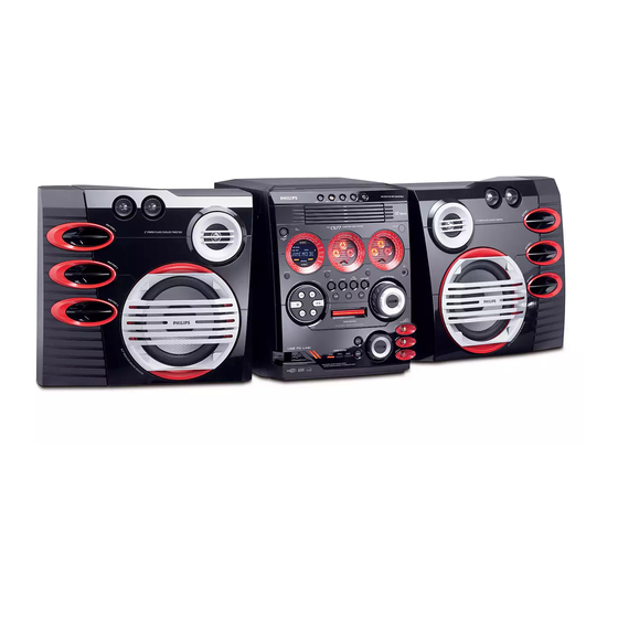
Mini System
Service
Service
Service
Service
Service
Service Manual
©
Copyright 2003 Philips Consumer Electronics B.V. Eindhoven, The Netherlands
All rights reserved. No part of this publication may be reproduced, stored in a retrieval system or
transmitted, in any form or by any means, electronic, mechanical, photocopying, or otherwise
without the prior permission of Philips.
Published by BB 0310 Service Audio
Version 1.1
TABLE OF CONTENTS
Location of pc boards & Version variations ................ 1-2
Technical Specifications ............................................. 1-3
Measurement setup .................................................... 1-4
Service Aids, Safety Instruction, etc. .......................... 1-5
Disassembly Instructions & Service positions .............. 2
Service Test Programs .................................................. 3
Set Block diagram ...................................................... 4-1
Set Wiring diagram ..................................................... 4-2
Front Control Board ....................................................... 5
Front Display Board ....................................................... 6
ECO6 Tuner Board : Systems Non-Cenelec ............. 7A
AF11 Board .................................................................... 8
P2003 135/165W Module .............................................. 9
5DTC Module (Basic Version) ..................................... 10
Set Mechanical Exploded view & parts list ................. 11
Document History ........................................................ 12
Printed in The Netherlands
Subject to modification
FW-C577/
Page
CLASS 1
LASER PRODUCT
GB
21/30/37
COMPACT
DIGITAL AUDIO
3139 785 30301
Advertisement
Chapters
Table of Contents


Need help?
Do you have a question about the FW-C577/21 and is the answer not in the manual?
Questions and answers