Table of Contents
Advertisement
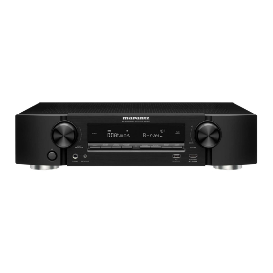
AV Surround Receiver
NR1607
• For purposes of improvement, specifications and design are subject to change without notice.
• Please use this service manual with referring to the operating instructions without fail.
• Some illustrations using in this service manual are slightly different from the actual set.
Service Manual
Click here!
On-line service parts list
http://dmedia.dmglobal.com/Document/DocumentDetails/23028
Online Parts List
(P5 to P7)
WEB owner's manual
http://manuals.marantz.com/NR1607/NA/EN/index.php
http://manuals.marantz.com/NR1607/EU/EN/index.php
http://manuals.marantz.com/NR1607/JP/JA/index.php
CAUTION IN SERVICING
ELECTRICAL
MECHANICAL
REPAIR INFORMATION
UPDATING
Please refer to the MODIFICATION NOTICE.
Confidential
1
Ver. 3
Advertisement
Table of Contents

Related Manuals for Marantz NR1607


Summary of Contents for Marantz NR1607
- Page 1 Service Manual Ver. 3 AV Surround Receiver Click here! NR1607 On-line service parts list http://dmedia.dmglobal.com/Document/DocumentDetails/23028 Online Parts List (P5 to P7) WEB owner’s manual http://manuals.marantz.com/NR1607/NA/EN/index.php http://manuals.marantz.com/NR1607/EU/EN/index.php http://manuals.marantz.com/NR1607/JP/JA/index.php CAUTION IN SERVICING ELECTRICAL MECHANICAL REPAIR INFORMATION UPDATING • For purposes of improvement, specifications and design are subject to change without notice. Please refer to the MODIFICATION NOTICE.
-
Page 2: Caution In Servicing
CAUTION IN SERVICING SAFETY PRECAUTIONS NOTE FOR SCHEMATIC DIAGRAM NOTE FOR PARTS LIST INSTRUCTIONS FOR HANDLING SEMICONDUCTORS AND OPTICAL UNIT Online Parts List Accessing the Parts List Logging in to New SDI and Accessing the Parts List Accessing the Part List from the Model Asset Screen PRINTED CIRCUIT BOARDS Parts Table Downloading the Parts List as an Excel File Revision History... -
Page 3: Safety Precautions
SAFETY PRECAUTIONS ◎ Make a safety check after servicing! The following items should be checked for continued protection of the customer and the service Check that all screws, parts and wires removed or disconnected when servicing have been put back technician. -
Page 4: Note For Schematic Diagram
NOTE FOR SCHEMATIC DIAGRAM WARNING: Parts indicated by the z mark have critical characteristics. Use ONLY replacement parts recommended by the manufacturer. CAUTION: Before returning the set to the customer, be sure to carry out either (1) a leakage current check or (2) a line to chassis resistance check. - Page 5 Online Parts List Accessing the Parts List Logging in to New SDI and Accessing the Parts List (1) Click the URL link on the cover of the service manual. (1) Access New SDI from the URL below. Examples of display <http://dmedia.dmglobal.com>...
-
Page 6: Revision History
Accessing the Part List from the Model Asset Screen Downloading the Parts List as an Excel File (1) Display Model Asset from New SDI. (1) Displays the Parts List. Click the Download icon. (2) Click the section displayed as ▼ Link to Part Lists under the model name. NOTE : If the ▼... - Page 7 Searching Part Numbers or Ref. Numbers You can search a Parts List for part numbers or Ref. numbers. (1) Enter the part number or Ref. number in the search window of the Parts List, and press the search button. (2) The search results are displayed. The name of the sheet in which the search part is used and the part’s line are displayed.
-
Page 8: Initializing This Unit
CAUTION IN SERVICING. Initializing This Unit Make sure to initialize this unit after replacing the microcomputer or any peripheral equipment, or the digital PCB. 1. Press the power button to turn off the power. 2. While holding down buttons "ZONE2 SOURCE" and "INTERNET RADIO" simultaneously, press the power button to turn on the power. -
Page 9: Schematic Diagrams
ELECTRICAL SCHEMATIC DIAGRAMS PRINTED CIRCUIT BOARDS SCH01_HDMI SW1 HDMI, F HDMI SCH02_HDMI SW2 SCH03_NET_PHY SPK, SIDE CNT, HDMI GUIDE A, HDMI GUIDE B SCH04_CPU_LEVEL_CHG AMP, FRONT, MC HP, USB SCH05_DIGITAL_CNT REG, GUIDE L, TOP GUIDE, FRONT CNT, REG CNT, SMPS SCH06_CPU SCH07_FRONT HDMI LEVEL DIAGRAM... - Page 10 SCHEMATIC DIAGRAMS SCH01_HDMI SW1 HDMI SW1 N1000 N1000 KYOSERA 1.0-16-23PB HPDF R1000 HPD8 TXEN TXEN DDCA_SDA RXF_DDCDA DDCA_SCL RXF_DDCCL HDMI5V RXF_5V STBY5V CEC5V FROM CEC5V_1 CEC3.3V D.SUPPLY CEC3.3V CEC3.3V L1000 CB05YTYH221 CEC1.1V1 DGND L1016 DGND DGND CB05YTYH221 RX_C- RXF_C- RX_C+ TO 0A RXF_C+ DGND...
- Page 11 SCH02_HDMI SW2 HDMI SW2 N1004 A0D7ABAR1990 R1105 RX4_5V HP_DET Q1009 HPD4 DDC_SDA RT1N141C Q1010 FROM DDC_SCK RT1N441C CEC5V_1 D.SUPPLY R1107 CEC3.3V RX4_DDCDA L1007 CB05YTYH221 CEC1.1V2 CE_REMOTE R1108 RX4_DDCCL L1019 DGND TXC- RX4_C- TO 6A CB05YTYH221 TXC_SHLD TXC+ RX4_C+ TX0- RX4_0- TX0_SHLD TX0+ RX4_0+...
- Page 12 SCH03_NET_PHY NET PHY TO 1B TO CPU DM920_SPDIF NET/USB_MCK NET/USB_LRCK DIR/A.PLD NET/USB_BCK NET/USB_DATA_/FR NET/USB_DATAF/FL TO 2B FROM NET3.3V NET2.5V D.SUPPLY NET1.8V NET1.25V.. DGND TO 3B R1207 OPEN R1208 OPEN NET3.3V C1172 OPEN-1608 920PCK C1173 100N-K 920VD0 C1174 1N-K 920VD1 U1005 MFI337S3959 920VD2 920VD3...
- Page 13 SCH04_CPU_LEVEL_CHG CPU LEVEL CHG TO 5B TO DIGITAL CNT REMOTE3.3V FROM SWM3.3V D.SUPPLY M3.3V DGND TO 6B SWM3.3V R1366 DGND R1379 R1385 OPEN OPEN 14 13 12 TO CPU TO 7B GND LINE POWER+ LINE POWER- LINE ANALOG AUDIO DIGITAL AUDIO TMDS SIGNAL VIDEO SIGNAL COMPONENT (Y)
- Page 14 SCH05_DIGITAL_CNT TO 9B DIGITAL CNT TO D.SUPPLY C1312 C1311 OPEN OPEN N1014 N1014 TO CP5203 C125Z2-23 DAC_FL+ DAC_FL- DAGND DAGND DAC_FR+ DAC_FR- DAGND DAGND CEN+ DAC_C+ DAC_C- CEN- DAGND DAGND DAC_SW+ N1039 DAC_SW- INPUT DAGND DAGND N1039 DAC_SL+ C125Z2-25 DA+5V DAC_SL- H/PL H/P_L...
- Page 15 C1353 100N-K AMPSIG_DET AMPSIGDET VCC_USB R2182 R1524 MODE AEXP DATA AEXP_DATA 33*4(AR) KEY3 KEY3 174:VREFH0 AEXP CLK AEXP_CLK OPEN NR1607/U1B 175:AVCC0 U1061 U1062 KEY2 KEY2 AEXP OE AEXP_OE 176:H/P DET MC14094BDTR2G MC14094BDTR2G NR1607/N1B OPEN KEY1 KEY1 AEXP STB AEXP_STB PRE_Z2_MUTE...
- Page 16 SCH07_FRONT HDMI FRONT HDMI FRONT HDMI B'D FRONT HDMI (FFC WAFER) R1552 R1546 R1547 R1549 OPEN R1548 OPEN R1551 OPEN Q1046 RT1N141C .HPA_D.. HP_DET Q1047 RT1N441C N1038 DDC_SDA DDC_SCK N1038 KYOSERA 1.0-16-23PB CE_REMOTE .CEC .CEC TXC- .HPA_D.. HPDF TXC_SHLD .TX_EN. TXC+ TX_EN TX0-...
- Page 17 SCH08_ADV8003 ADV8003 DV5V FROM DV3.3V D.SUPPLY DV1.8V DGND PVDD5_TX DVDD_TX AVDD3_1_TX PVDD_TX PVDD3_TX AVDD2_TX L1042 L1041 L1038 L1039 L1040 CB05YTYH221 L1043 TO 8C CB05YTYH221 CB05YTYH101 CB05YTYH221 CB05YTYH221 CB05YTYH221 TX1_C- TX1_C- TX1_C+ TX1_C+ TX1_0- TX1_0- TX1_0+ TX1_0+ TX1_1- TX1_1- TO HDMI TX DDR_1.8V PVDDR_TX AVDD3_3_TX...
- Page 18 SCH09_ADV8003 DDR ADV8003 DDR TO D1 TO D2 ADV8003 TO D3 ADV8003 ADV8003 U1028 A3R12E40CBF-8E(512Mb) U1029 A3R12E40CBF-8E(512Mb) DDR1 DDR2 DDR_1.8V DDR_1.8V DGND DGND DR_TXDQSB1 DDR_1.8V DDR_1.8V DGND DGND DR_TXDQSB3 DDR_1.8V DR_TXDQ14 DGND DR_TXDM1 DR_TXDQS1 DGND DR_TXDQ15 DR_TXDQ30 DGND DR_TXDM3 DR_TXDQS3 DGND DR_TXDQ31 DDR_1.8V...
- Page 19 SCH10_D.SUPPLY CEC3.3V M3.3V D3.3V2 SWM3.3V DA1.0V REMOTE3.3V DV1.8V NET3.3V DA3.3V DV3.3V D.SUPPLY DGND DGND DGND L1054 CB05YTYH221 L1055 CB05YTYH221 L1056 CB05YTYH221 M3.3V N1033 HDMI TX ES START : OPEN L1138 1.5A R1947 OPEN 2.2UH N1033 L1112 R1946 OPEN YMW025-06R CEC1.1V CEC1.1V TO 4D R1812...
- Page 20 SCH11_HDMI TX HDMI TX CEC5V_2 CEC5V_1 CEC3.3V CEC1.1V DGND VDD33IO L1115 CB05YTYH221 TO D4 AVDDH33 L1082 AVDD11 CB05YTYH221 L1083 CB05YTYH221 VDD33 L1084 CB05YTYH221 VDD11_1 L1085 CB05YTYH221 PVDD33 L1086 CB05YTYH221 N1030 N1030 AVDD33 L1087 OPEN-A0D7ABAR1990 FBMJ3216HL160NT AVDD11RX_2 L1088 FBMJ3216HL160NT TX2+ P0TX0_2+ R1984 L1116 TX2 SHIELD...
- Page 21 SCH12_DIR_A.PLD DIR/A.PLD TO A5 TO B0 TO 8D TO B2 TO D7 TO C6 FROM FROM HDMI SW1 FROM HDMI SW2 NET PHY HDMI TX ADV7850 DIR input CH1:D-DATA *FILTER COMPONENTS VALUE TYPE TOLERANCE R1907 Ω METAL FILM OR CARBON Ω...
- Page 22 SCH13_DSP TO E0 TO C5 TO DIR/A.PLD TO CPU MP OPEN N1034 1.0-16-6PB-2 R2099 R2100 DSP1CS R2079 DSP1MISO DSP1MOSI DSP1CLK DGND R2098 DSP input DATA DA3.3V 19 18 17 SPDIF(PCM2ch) I2S(HD Audio) I2S(PCM Multi) DSP1INF/FL L/R(from DIR) I2S0 FL/FR DSP1IN_/FR ------ ------ ------...
- Page 23 SCH14_MAIN DAC TO E1 TO D9 TO C7 TO E2 MAIN DAC FROM FROM FROM FROM DIR/A.PLD DIR/A.PLD DIR/A.PLD DA+5V A/DIN_R DAGND A/DIN_L DAGND 100N-K-1608 R1997 DACRTNGND R1998 100N-K-1608 DA+5V C2137 R1999 DAGND OPEN-1608 100-1608 DAGND R2002 TO DIGITAL CNT C2143 10U-K-2012 100-1608...
- Page 24 SCH15_ADV7850 ADV7850 DV5V 680mA DV3.3V 1620mA DV1.8V TO D5 DGND L1090 C2187 100N-K VIN8 CB05YTYH221 TVDD C2188 100N-K VIN9 3.3V 400mA C2189 100N-K VIN7 1Vp-p C2202 1N-K SYNC2 R2089 24-1608 C2203 100N-K DECIN_Y VIN4 U1055 R2090 24-1608 C2204 100N-K DECIN_CR VIN5 ADV7850 3.3V 20mA...
- Page 25 R4004 C4004 47N(M)-50V 47N(M)-50V ※ CAPACITOR OPTION CN4003 OPTION A OPTION B 0(3216) R4059 U1B/FB N1SG, N1B U1B/FB N1SG, N1B L4005 SP-2507 NR1607 100NF 2200PF 0.01UF R4012 D4020 RLY4003 10(2) R4005 10(1/5) C4013 LBAS16HT1G JZC-42F C4032 47N(M)-50V C4005 OPTION A...
- Page 26 SCH17_CNT SPK_SCNT 2/2 SIDE CONNECTOR TO MX/RC-5 N4600 1.0-11S-4PW OPEN R4638 REMOTE3.3V R4637 MI232O R4636 MO232I M/DGND CP4604 HDMI DIGITAL CNT E5 HDMI DIGITAL CNT E3 ON/OFF JACK4602 TO N1016 ZD4700 C4704 PJ-308-02 (BK) ZJ16B 100N-K TRIGGER PJ-308-02 C4705 100N-K CP4604 D4703 LBAS16HT1G...
- Page 27 SCH18_INPUT CP5200 CP5201 CP5202 CN5200 CN5203 CN5201 AV 1/3 SIDE_CNT 2/4 I9 SIDE_CNT 2/4 D9 SIDE_CNT 2/4 F9 FRONT_CNT 3/4 J8 TO CP4000 TO CN4606 TO CP4002 TO CN4603 TO CN4602 REF : 5200-5399 TO CP4614 SPK_SMPS 1/2 A9 CN5203 50MM/5P CP5202 1.25B-2-11A...
- Page 28 SCH19_VIDEO AV 2/3 REF : 5400-5499 CN5402 CVBS INPUT SW NJM2595MTE1 u-COM CON IC CON OUT PUT NR1607 VINA VINB VINC JK5401_4 IN 1 MUTE MONITOR IN 2 MUTE IN 3 CBL/SAT IN 4 IN 5 BLU-RAY R5403 OPEN R5442...
- Page 29 SCH20_TUNER AV 3/3 REF : 5500-5599 IC4006 AZ1117-3.3 TUNER PACK R5501 R5502 C5500 OPEN RICOH TUNER R5514 OPEN R5504 IISD(N.C) TU_IISD TUNERL TUNERL TUNERR TUNERR TU_IISD R5506 TU_GND R4075 TUNERL. BD5500 CB03YTYN121 R5511 R4074 TU_3V3 TU_3.3V. AGND R5508 OPEN R4073 C5507 OPEN TU_DA...
- Page 30 SCH21_FRONT NR1607 FRONT B`D FRONT 1/1 R4403 R4410 REF: 4400-4599 R4409 OPEN R4400 R4410 C4410 OPEN TUNED STEREO SLEEP R4403 AUTO HDMI DIGITAL ANALOG S.BACK FIL2 R4401 OPEN MUTE R4404 OPEN FIL1 D4400 R4402 OPEN F4400 1N4007 4R7(1) DIG. ANA.
- Page 31 SCH22_AMP1 7CH_AMP 1/2 REF : 4800-5199 NR1607 AMP B'D 1/2 39.6V R4800 R4802 ZD4800 R4801 R4803 R4804 C4800 ZJ5.1A 100K 5K6(1) DHPTF1608-105T 100N-K C4803 Q4800 C4802 47/50_KOSHIN TP4800 39.1V OPEN R4809 C4801 R4805 KTA1024Y 0.6V 1.1V 680K 10N-K Q4801 R4806...
- Page 32 R4972 C4858 R4968 R4969 R4970 2N2-K Q4836 470P-500V 22(1) 2SB1560 Q4837 R4971 KTC3206Y C4860 OPEN C4862 C4861 R4973 NR1607 AMP B'D 2/2 OPEN OPEN R4974 1K2(1) 47(1) R4977 R4975 ZD4812 R4976 R4978 R4979 C4863 ZJ5.1A 100K 5K6(1) DHPTF1608-105T 100N-K C4865...
- Page 33 SCH24_SMPS SMPS_REG_FCNT 1/3 NR1607 SMPS B'D OPTION L4141 C4148 0.01UF/250V OPTION OPTION L4140 OPEN F4140 SQ2014 BLACK JP4140 JUMPER D4142 1N4007 live ZD4151 JK4140 D4143 1N4007 ZD4147 ● ● ZJ22B Neutral ZJ39B WHITE ZD4152 ● ● D4144 1N4007 ZD4148 ZJ22B...
- Page 34 SCH25_REG SMPS_REG_FCNT 2/3 NR1607_REG REGULATOR B'D D4608 OPEN CN4607 CN4607 120MM/4P IC4604 KIA7805API VIDEO+5V VIDEO_+5V FRONT CONNENCTOR VIDEO_GND C4610 (REG_CNT 3/4 M7) VIDEO_GND C4606 D4604 4700/16(16*25) R4600 VIDEO-5V 10/50 1SS133 OPEN TO CP4615 C4611 R4601 C4607 D4605 3300/16(12.5*25) OPEN 10/50 1SS133 VIDEO_-5V IC4602...
- Page 35 SCH26_FRONT CNT SMPS_REG_FCNT 3/3 FRONT CONNECTOR CP4613 HDMI DIGITAL CNT E8 TO N1039 CP4613 1.25B-2-25A TO HDMI CP4615 CP4615 20010WR-04 VIDEO+5V VIDEO_GND SMPS_REG_RC5_FCNT 2/4 B3 VIDEO_GND VIDEO-5V TO CN4607 CP4611 CP4614 CP4614 CP4611 1.25B-2-11A 1.25B-2-21A TO AV B'D TO CN5402 TO CN5200 AV 2/3 M4 AV 1/3 K1...
- Page 36 PRINTED CIRCUIT BOARDS HDMI, F HDMI Lead-free Solder When soldering, use the Lead-free Solder (Sn-Ag-Cu). HDMI (A SIDE) F HDMI (A SIDE) F HDMI (B SIDE) C1764 L1147 N1019 N1039 C1778 C1779 L1110 C1841 N1017 N1000 L1080 C1760 C1782 L1109 H/P_DET L1081 C1781...
- Page 37 AV (A SIDE) AV (B SIDE) 1.D5V(RC-5) 2.KILLIR 3.RC_OUT 4.FRONT IRIN 5.RC_IN 6.MVOLDATA 7.MVOLCLK 8.M3.3V 9.M/DGND 10.M/DGND 11.TU_IISD R5520 12.TU_IIC/RDSI 13.TU_LA 14.TU_DA 15.TU_CK R5568...
- Page 38 SPK, SIDE CNT, HDMI GUIDE A, HDMI GUIDE B SPK (A SIDE) SPK (B SIDE) C4052 C4047 C4035 C4034 C4040 C4046 C4043 C4045 C4042 C4051 C4048 C4036 C4033 C4039 RLY4003 C4044 C4041 C4050 C4049 C4037 C4032 C4038 C4018 R4059 D4020 C4025 C4021 C4020...
- Page 39 RADI THERMAL C4850 R4963 R4927 R4851 C4895 TR THERMAL Q4806 R5009 R4886 R5051 C4893 Q4825 Q4820 R5000 R5050 R5082 R4958 J4917 NR1607 (6P) C4853 R4977 C4879 R5018 Q4852 Q4853 R4922 Q4817 Q4800 R4845 R5095 NR1506/NR1606(7P) C4836 Q4810 R5064 R4895 R4887 J4898...
- Page 40 REG, GUIDE L, TOP GUIDE, FRONT CNT, REG CNT, SMPS REG (A SIDE) REG (B SIDE) GUIDE L (A SIDE) TOP GUIDE (A SIDE) FRONT CNT (A SIDE) FRONT CNT (B SIDE) CLP4603 SCREW 3*8 JP4631 CN4615 CP4615 CLP4606 J4667 7812 J4669 J4652...
-
Page 41: Level Diagram
LEVEL DIAGRAM FRONT ch AVR-S920W/X2300W SR5011,NR1607 LEVEL DIAGRAM FRONT ch BD34704 ANALOG H/POUT SPEAKER LINE IN + GAIN + ADJ. PCM1690 + PCM9211 + - - ZONE2 (AVRX2300,SR5011 ONLY) +30dB BD34704 MAX. OUTPUT 4.2Vrms Differential Out PCM1690 SP OUT 4.23Vrms/8Ω 0dBFS MAX SIGNAL LEVEL 0dBFS = +/-4.0Vpp=2.83Vrms... - Page 42 CENTER ch AVR-S920W/X2300W SR5011,NR1607 LEVEL DIAGRAM CENTER ch BD34704 SPEAKER + GAIN ADJ. PCM1690 + + - - +30dB BD34704 MAX. OUTPUT 4.2Vrms Differential Out PCM1690 SP OUT 4.23Vrms/8Ω 0dBFS MAX SIGNAL LEVEL 0dBFS = +/-4.0Vpp=2.83Vrms +20dB +20dB DOLBY LIMIT LEVEL (ALLch-3dBFS)
- Page 43 SUBWOOFER ch AVR-S920W/X2300W SR5011,NR1607 LEVEL DIAGRAM SUBWOOFER ch BD34704 MUTE PRE OUT GAIN ADJ. PCM1690 + + - - +30dB BD34704 MAX. OUTPUT 4.2Vrms MAX SIGNAL LEVE Differential Out PCM1690 DOLBY LIMIT LEVEL(ALLch-3dBFS) 0dBFS 0dBFS = +/-4.0Vpp=2.83Vrms +20dB +20dB -10dBFS +10dB +10dB...
- Page 44 SURROUND ch AVR-S920W/X2300 SR5011,NR1607 LEVEL DIAGRAM SURROUND ch BD34704 SPEAKER + GAIN ADJ. PCM1690 + + - - +30dB BD34704 MAX. OUTPUT 4.2Vrms Differential Out PCM1690 SP OUT 0dBFS 4.23Vrms/8Ω MAX SIGNAL LEVE 0dBFS = +/-4.0Vpp=2.83Vrms +20dB +20dB DOLBY LIMIT LEVEL(ALLch-3dBFS) +29dB...
- Page 45 SURR.BACK ch AVR-S920W/X2300W SR5011,NR1607 LEVEL DIAGRAM SURR.BACK ch BD34704 + SPEAKER GAIN PCM1690 + + - - +30dB BD34704 MAX. OUTPUT 4.2Vrms SP OUT Differential Out 4.23Vrms/8Ω PCM1690 0dBFS 0dBFS = +/-4.0Vpp=2.83Vrms MAX. SIGNAL LEVEL +20dB +20dB DOLBY LIMIT LEVEL(ALLch-3dBFS) +29dB -10dBFS...
- Page 46 ZONE2 AVR-S920W/X2300W SR5011,NR1607 LEVEL DIAGRAM ZONE2 BD34704 from F-ch from SPEAKER DA SB-ch + LINE IN + MAIN NET/USB DAC + ZONE2 +30dB SP OUT 4.48Vrms/8Ω 0dBFS PCM5100 2.0Vrms MAX SIGNAL LEVEL 2.00Vrms +20dB +20dB 0dBFS -10dBFS +10dB +10dB -20dBFS(DIG.IN) -2.0dB...
-
Page 47: Block Diagram
BLOCK DIAGRAM ANALOG AUDIO DIAGRAM ANALOG AUDIO DIAGRAM H/P-L HEADPHONE OUT TO DIGITAL AUDIO BLOCK TO DIGITAL AUDIO BLOCK TO DIGITAL AUDIO BLOCK H/P-R SPK OUT SBL(FL-B/FL-H/BI-AMP/ZONE) SBR(FR-B/FR-H/BI-AMP/ZONE) DM920_R/L ANA_FL DSP_FL ANALOG ANA_FR SAT_CBL INPUT DSP_FR 2.2ch PREOUT DSP_C TUNER DSP_SW FM/AM MIC(Mini Jack) - Page 48 DIGITAL AUDIO DIAGRAM DIGITAL AUDIO DIAGRAM TMDS TMDS TMDS HDMI OUT OUT0 OUT1 ADV8195 HDMI2.0 TX FRONT TMDS MN864788 HDMI BUFFER SW1_SD0 SW1_SD1 SW1_SD2 HDMI1 HDMI2.0 RX SW1_SD3_SPDIF MN864788 (2.2 4 INPUTS) SW1_LRCK HDMI2 SW1_BCLK SW1_MCLK HDMI3 AD55/058Z-0 TMDS HDMI RECEIVER (ADV8003-8B) HDMI IN ADV7850...
- Page 49 VIDEO DIAGRAM VIDEO DIAGRAM ADV8195 FRONT HDMI TMDS IN BUFFER OUT0 TMDS OUTPUT HDMI OUT TMDS IN HDMI1 HDMI2.0 RX MN864788 HDMI2.0 TX (2.2 4 INPUTS) MN864788 HDMI2 MX25L12835FMI HDMI IN TMDS OUT TMDS IN HDMI3 OUT1 HDMI4 TMDS OUT HDMI5 OUT0 HDMI RECEIVER...
-
Page 50: Power Diagram
POWER DIAGRAM MAIN +B S1(AMP +B) MAIN -B A+7.0V KIA7808API DA+5.0V(PCM1690/PCM9211) KIA7805API AP7361 DA+3.3V(PCM5100) A-7.0V KIA7908PI S2(+8V,-8V) KIA7805API V+5.0V R4032 JUMPER TUNER+3.3V AZ1117-3.3 RELAY MAIN TRANS KIA7905PI V-5.0V FL AC (F1) FL AC (F2) R1825 SWM5V FL5V M3.3V (CPU) AP7361 AC CORD STBY3.3V CEC_POWER2... -
Page 51: Wiring Diagram
WIRING DIAGRAM HDMI PCB MAIN + SPK PCB FRONT CNT PCB AV PCB SMPS PCB REG-CNT PCB REG PCB AMP PCB FRONT PCB HP + MC PCB USB PCB FRONT HDMI PCB PLATE PLATE PLATE... - Page 52 WHITE LED(X2300(NA))/ GREEN PF5/IRQ4 POWER LED control pin LED(X2300(EU/ CH/JP)/S920/ SR5011/NR1607) E20 Emulator control pin (On chip Emulator is used,this EMLE EMLE pin should be High. Not used,it should be Low) VSEL A Master Volume (Rotary encoder) signal input pin...
- Page 53 PC1/SCK5/IRQ12 DAC.PLD ERR Detect PLD error (from Audio PLD) P87/TXD10/TIOCA2 Remote code (RC-5) output pin OUT(SR5011/ Power supply pin NR1607) PC0/IRQ14 H/P RL Headphone relay control pin Ethernet(CY920) RESET control pin (Set to NMOS open- P16/TXD1/RXD3/ E RESET O(ODR) N3VPu...
- Page 54 DIR RST DIR (PCM9211) control pin PD5/IRQ5/AN113 788_2_HAINT HDMI Rx (MN864788) audio interrupt signal det SDA(X2300)/ PD4/IRQ4/AN112 I_O/O HDMI TMDS switch I2C ccontrol pin for TMDS261B NC(NR1607/ 3VPu SR5011) RST(NR1607/ SR5011)/ Video decoder (ADV7850) reset control pin NC(X2300/ S920) PD3/IRQ3/AN111...
- Page 55 PCM9211 www.ti.com SBAS495 – JUNE 2010 AD8195 PIN CONFIGURATIONS AD8195ACPZ (HDMI : U1022) PCM9211 (HDMI : U1040) PT PACKAGE LQFP-48 PIN CONFIGURATION AND FUNCTION DESCRIPTIONS (TOP VIEW) ERROR/INT0 VDDRX 30 AVCC PIN 1 30 AVCC NPCM/INT1 RXIN1 29 PE_EN INDICATOR PIN 1 29 PE_EN INDICATOR...
- Page 56 PCM9211 PCM9211 BLOCK DIAGRAM www.ti.com SBAS495 – JUNE 2010 BLOCK DIAGRAM DESCRIPTION NAME FILT TOLERANT AUXIN 0 24 MDI/SDA Software control I/F, SPI data input / I2C data input/output(2) AUTO RXIN7 RXIN 0 RXIN0 SCKO DOUT RXIN 1 RXIN1 MAIN OUTPUT RXIN 2 RXIN2...
- Page 57 CS49844A (HDMI : U1073) W9864G6KH-5 (HDMI : U1023) SD_A3, EXT_A3, DAO3_D3, XMTA, GPIO113 SD_A2, EXT_A2 SD_D11, EXT_D3 SD_A1, EXT_A1 SD_D12, EXT_D4 SD_A0, EXT_A0 SD_D13, EXT_D5 SD_A10, EXT_A12 GNDIO4 SD_BA0, EXT_A13 VDDIO4 W9864G6KH SD_BA1, EXT_A14 SD_D14, EXT_D6 SD_CS, EXT_OE SD_D15, EXT_D7 SD_RAS, EXT_CS1 SD_D0, EXT_D8 SD_CAS, EXT_CS2...
- Page 58 PCM1690 (HDMI : U1048) W9864G6KH-5 Block diagram CLOCK BUFFER CONTROL SIGNAL GENER ATOR COMMAND DECODER COLUMN DECODER COLUMN DECODER CELL ARRAY CELL ARRAY BANK #0 BANK #1 MODE REGIST ER SENSE AMPLIFIER SENSE AMPLIFIER ADDRESS BUFFER DATA CONTROL CIRCUIT BUFFER COLUMN PCM1690 Pin Function REFRESH...
- Page 59 PCM1690 SBAS448A – OCTOBER 2008 – REVISED JANUARY 2009.............................. www.ti.com FUNCTIONAL BLOCK DIAGRAM PCM1690 FUNCTIONAL BLOCK DIAGRAM TERMINAL PULL- DESCRIPTION DOWN TOLERANT NAME Control port mode selection. Tied to VDD: SPI, left VOUT1+ DIN1 MODE DIN2 open: H/W mode, tied to DGND: I2C VOUT1- DIN3 Audio Interface...
- Page 60 PCM5100, PCM5101, PCM5102 マイクロステップボリュームにより、 不快なボリューム切替えノイズを軽減 ゾーン 3 対応 SLAS764 – MAY 2011 www.ti.com ゾーン用の 2ch ボリューム搭載 DEVICE INFORMATION 2 線シリアルバスコントロールは、3.3/5V に対応 SQFP-T80C TERMINAL FUNCTIONS, PCM510x 用途 PCM5100 (HDMI U1052) BD34704KS2 (AV : IC4200) AV レシーバ、ホームシアタシステムに最適。 PCM510X (top view) 基本アプリケーション回路...
- Page 61 G Crosstalk -65dBtyp. G Internal 6dB Amplifier WIDE BAND 3-INPUT 1-OUTPUT 3-CIRCUIT VIDEO AMPLIFIER G Internal 75Ω Driver G Bipolar Technology G Package Outline DIP16,DMP16 GENERAL DESCRIPTION PACKAGE OUTLINE 2. FL DISPLAY The NJM2586A is a wide band 3-input 1-output 3-circuit video I PIN CONFIGURATION and BLOCK DIAGRAM NJM2595MTE1 (AV amplifier.
- Page 62 MECHANICAL DISASSEMBLY Flowchart 1. COVER 2. FRONT PANEL ASSY 3. RADIATOR ASSY 4. HDMI PCB 5. SPK PCB 6. TRANS 7. SMPS PCB 8. REG PCB 9. AV PCB EXPLODED VIEW PACKING VIEW...
- Page 63 DISASSEMBLY Flowchart • Remove each part following the flow below. • Reassemble the removed parts in the reverse order. • Read "SAFETY PRECAUTIONS" before reassembling the removed parts. • If wire bundles are removed or moved during adjustment or part replacement, reshape the wires after completing the work. Failure to shape the wires correctly may cause problems such as noise. •...
- Page 64 • The photographs with no shooting direction indicated were taken from the top of the unit. (1) Remove the PCB HOLDER. Remove the screws. Remove the TAPE. • Photos of NR1607 U are used in this manual. The viewpoint of each photograph...
- Page 65 3. RADIATOR ASSY 4. HDMI PCB Proceeding : TOP COVER → COVER → RADIATOR ASSY Proceeding : TOP COVER → COVER → HDMI PCB (1) Remove the screws. (1) Remove the screws. View from the bottom Shooting direction: C Shooting direction: D Shooting direction: A (2) Cut the wire clamps, then remove the CORD HOLDERs and connectors.
- Page 66 5. SPK PCB 6. TRANS Proceeding : TOP COVER → COVER → HDMI PCB → SPK PCB Proceeding : TOP COVER → COVER → HDMI PCB → TRANS (1) Remove the screws. (1) Remove the CORD HOLDERs and connector wires. from CP4401 Shooting direction: A CP4607...
-
Page 67: Exploded View
EXPLODED VIEW http://dmedia.dmglobal.com/Document/DocumentDetails/23028 Parts List: S 1 - S 9 - S 1 3 S 1 - S 7 - S 1 3 S 2 - S 1 4 S 4 - S 1 6 S 1 2 S 2 -1 S 5 - S 2 - S 6 -1... -
Page 68: Packing View
ZIPPERBAG(A4size) ZIPPERBAG(A5size) Notes on RADIO (ALL) SPOTIFY insertion sheet SAFETY INST. (ALL) dts : User update insertion (marantz) JAPAN POSTCARD (F only) INST. MANUAL (CD) (F only) WARRANTY USA & CANADA (U only) Update insertion sheet (U only) SPK WIRE LABEL (ALL) -
Page 69: Troubleshooting
REPAIR INFORMATION TROUBLE SHOOTING SPECIAL MODE 1. POWER Special mode setting button 2. Analog video 1. Version Display Mode 3. HDMI/DVI 2. PANEL / REMOTE LOCK Selection Mode 4. AUDIO 3-1. Selecting the Mode for Service-related 5. Network / Bluetooth / USB 3-2. - Page 70 TROUBLE SHOOTING 1. POWER 1.1. The unit does not power on 1.2. Fuse is blown The unit does not power on Blown fuse Does the power indicator on the front panel Does the power indicator on the front Check the rectifier diode in the Check for short circuits between flash in green or white when the power is turned panel flash in red when the power is turned...
-
Page 71: Analog Video
2. Analog video COMPONENT / HDMI OUT NG Input CVBS / COMPONENT Input CVBS Input COMPONENT Input Function : CBL / SAT Function : CBL / SAT HDMI Check the input signal to the VIDEO DECODER. Can a signal be confirmed at the following To "A"... - Page 72 Input Input CVBS COMPONENT Check the settings of each IC. Check the settings of each IC. Are the following voltages set? Are the following voltages set? HDMI PCB HDMI PCB faulty. HDMI PCB HDMI PCB faulty. N1039 - 12 pin : Hi (3.3 V) N1039 - 11 pin : Lo (0 V)
- Page 73 3. HDMI/DVI 3.1. No picture or sound is output (HDMI to HDMI) (8) When using a MARANTZ Blu-ray/DVD player, is the "HDMI" indicator of the fluorescent display lit? Proceed to YES when using a Blu-ray/DVD player produced by other manufactures.
- Page 74 (15) Are a picture and sound output when a dif- The TV is faulty. ferent TV is used? Check the unit. "HDMI "Rx/Tx" Failure Detection"...
- Page 75 4. AUDIO 4.1. AUDIO CHECK No audio output CHECK 1 INPUT SURROUND MODE SOURCE Check the ANALOG AUDIO BLOCK Audio output OK? ANALOG 2CH DIRECT ANALOG CHECK 2 INPUT SURROUND MODE SOURCE Check the DIGITAL AUDIO BLOCK Legacy Audio output OK? COAX or OPT (PCM or DolbyDigital or dts…) CHECK 3...
-
Page 76: Analog Audio
4.2. Power AMP (AMP PCB) 4.3. Analog audio No audio output. No audio output. Protection is activated. Is the power transistor open or short circuited? Is a voltage of ± 8 V supplied to INPUT PCB Replace the power transistor. Repair the ±... -
Page 77: Cannot Connect To The Network
5. Network / Bluetooth / USB 5.1. Cannot connect to the network Check the connection environment Can the D3.3V2 output volt- The circuit of D5V_POWER Insert the LAN cable correctly and then turn on Is D5V_POWER (U1018 uCOM Is the LAN cable correctly inserted? age (3.3 V) to U1067 (DC-DC between U1018 and U1067 the power again. - Page 78 5.2. Cannot establish a Bluetooth connection Can the NET2.5V output volt- The circuit of E_POWER2 be- Is E_POWER2 (U1018 uCOM age (2.5 V) to U1072 (DC-DC tween U1018 and U1072 are 133 pin) "Hi" ? Check the Bluetooth device being used Conv.) be confirmed? faulty.
- Page 79 5.3. Cannot recognize the connected USB device 5.4. No picture or sound is output Check the USB device being used Checking the unit (If no picture is output) Are digital video signals(920PCK, 920VD0 The circuit around CY920, U1026(ADV8003) is Is a USB hub being used? Do not use a USB hub.
- Page 80 HDMI test point USB test point C4442 C1778 C1764 L1147 N1019 N1039 C1779 L1110 CP4402 N1000 C1841 N1017 L1080 C1760 C1782 L1109 H/P_DET L1081 C1781 L1058 NPCK R1374 CP4402 C1295 R1369 C1293 R1361 Q1059 R1376 C1288 N1036 D_BSY C1850 R1672 R2002 C2102 R1673...
- Page 81 6. SMPS Operation waveform for each part DC 5V is not output. Primary drain After primary side rectification (Caution: High voltage, electric shock) (Caution: High voltage, electric shock) C4148 0.01UF/250V OPTION OPTION D4142 1N4007 ZD4151 D4143 1N4007 ZD4147 Replace the IC4140 ZJ22B ZJ39B Is IC4140 (TOP268VG) dam-...
- Page 82 HDMI "Rx/Tx" Failure Detection 1. Prior checking Check item (0) : Checking the HDMI connector Checking the condition of the HDMI pin (rear/front). There are deformed pins. Replace the HDMI connector. Check for deformed pins. None of the pins are deformed. 3.
- Page 83 Port: Select COM port of PC Baud rate: 19200bps Data bits: 8 Stop bits: 1 Parity: none Transmitted text Flow control: none Select Append CR-LF Forward: (none) Check the Local Echo check box. Figure 1 Device Connection Method (NR1607) Figure 3 Serial Port Setup Screen...
- Page 84 After exiting "Setup Assistant,” execute the above. 1. Input a command in the 2.Click on the transmission button. transmission command input. Press Figure 6-1. AVR settings (NR1607) Figure 8 Method for Sending Termite Commands All the for Volume 7 segment indicator Lights...
- Page 85 3. Starting detecting the point of failure 3-1 Check the "HDMI/DVI" item in troubleshooting. Check item(1). Is the GUI version readable correctly? Check item(4). Check that the version of the AVR can be read Go to check item (42) (2)-1 Turn Video Conversion "OFF" on the setup menu. correctly.
- Page 86 3-2 HDMI Rx (MN864788) failure detection procedure Checking device. (HDMI Rx) When the results of check item (7) are "the communication results are not OK" Check communication between CPU and the HDMI Rx device. Checking device. (HDMI Rx) Check item (7). : Check communication between CPU and the HDMI Example : Check the power supply voltage.
- Page 87 Checking the reset waveform (HDMI Rx) Check item(10). Checking the reset waveform : Check the waveform. Check the HDMI Tx. Is the waveform of the TP near the HDMI Rx (U1000 or U1003) Check the HDMI Rx1. Check the HDMI Rx2. Remove the damping resistor correct (like the one shown in the diagram) when the power is Remove the damping resistor...
- Page 88 When the results of check item (7) are "the communication results are OK" Checking operation between the HDMI (Rx) device and the player Check item(14). Checking the +5V/DDC status register : Example Send the following command from Termite.exe. HDMI Rx1 (When checking HDMI inputs 1, 2, and 3) Case of HDMI IN1 Send the command "i 002B 0084...
- Page 89 When the results of check item (13) are "00" When the results of check item (14) are "00 or 04" (Detection of 5V is not OK) (Detection of DDC is not OK.) Check the +5V voltage. (HDMI Rx) Check the DDC line. (HDMI Rx) Check item(15).
- Page 90 When the results of check item (14) are "22" (Detection of DDC is OK.) Checking the TMDS status register 3.3V TMDS Signal TMDS Check item(17). Checking register of the TMDS CLK detection status Example register : Send the following command from Termite.exe. Example of waveform in check ①...
- Page 91 3-3 Front HDMI Buffer IC (AD8195) failure detection procedure Checking operation between the HDMI (Front HDMI Buffer) and the player Checking the +5V/DDC status register (Front HDMI Buffer) Check item(22). Checking the 5 V status of the register : Example Send the following command from Termite.exe.
- Page 92 When the results of check item (22) are "00" When the results of check item (23) are "00 or 04" (Detection of 5V is not OK.) (If the DDC are not OK) Check the +5V voltage. (Front HDMI Buffer) Check the DDC line. (Front HDMI Buffer) Check item(24).
- Page 93 When the results of check item (23) are "22" (Detection of DDC is OK) Checking the TMDS status register Check item(26). Check the TMDS CLK detection status of the regis- Check item (27). Checking the TMDS input waveform. : Example ter.
- Page 94 3-4 HDMI transmission IC (MN864788) failure detection procedure Check the output terminal. No video signal is output from Monitor. Check item(28). Check the video output port for failure. : Checking device. HDMI (Tx) Check the Monitor output video signal is correct. Example Check the I2C communication line.
- Page 95 When the results of check item (29) are "the communication results are not OK" Check item(32). Check the reset of HDMI TX. : Checking the waveform. Is the waveform at the test point TP (U1039) correct when power is Checking device. (HDMI Tx) turned on? Check the power supply voltage.
- Page 96 Checking between Monitor and the TV. When the results of check item (29) are "the communication results are OK" Connect Monitor to the TV and check the following items with the TV turned on. Checking operation between the HDMI (Rx) device and the HDMI device (Tx). Checking the HPD/RXSENSE status register.
- Page 97 Example When the results of check item (35) are "30" (Detection of HPD is OK / Detection of RXSENSE is OK ) Checking the EDID register (Monitor) Check item(36). Check the Monitor EDID : ① Unplug the AC cord. Plug the AC cord into a power outlet. The first eight bytes are nor- ②...
- Page 98 When the results of check item (35) are "10" When the results of check item (35) are "20" (Detection of HPD is OK / Detection of RXSENSE is not OK ) (Detection of HPD is not OK / Detection of RXSENSE is OK ) Checking the RXSENSE (Monitor) Checking the HPD.
- Page 99 When the results of check item (35) are "00" (Detection of HPD is not OK / Detection of RXSENSE is not OK ) Check the RXSENSE/HPD. (Monitor1) Check item(41). Checking the HPD and RXSENSE. : Does the test point of RXSENSE close to the HDMI output terminal (N1031) indicate the 3.3 V? Does the test point of HPD close to the HDMI output terminal (N1031) indicate the Hi(3-5V) V?
- Page 100 3-5 GUI IC (ADV8003) failure detection procedure GUI failure detection procedure 1 When the results of check item (43) are "the communication results are not OK" Check item(42). Checking device. (GUI) Rewrite to the GUI ROM. Go to check item (3) After writing, is the GUI version readable cor- rectly? Check the power supply voltage.
- Page 101 Checking the reset waveform. Check the I2C communication line. Check item(48). Checking the reset. : Check item(49). Check the I2C communication line : Check the CPU. Check the CPU. 10ms Is the waveform of the TP near the GUI(U1026) correct (like the one Is the "I2C"...
- Page 102 GUI IC (ADV8003) failure detection procedure 2 Checking the TMDS status register (GUI -> HDMI Tx) Check item(51). Check the TMDS CLK detection status of the regis- Example ter. Send the following command from Termite.exe. Send the command "i 0006 00FF 0001".
- Page 103 3-6 HDMI SW IC (ADV7850) failure detection procedure Checking device. (HDMI SW) When the results of check item (53) are "the communication results are not OK" Check the I2C communication line. Checking device. (HDMI SW) Check item (53). : Check communication between CPU and the Example HDMI Rx device.
- Page 104 When the results of check item (53) are "the communication results are OK" Checking the TMDS status register (HDMI SW -> GUI) Example Check item(56). Check the TMDS CLK detection status of the regis- ter. : Send the following command from Termite.exe. Send the command "i 00E2 0004 0001".
- Page 105 4. Device implementation location HDMI (A SIDE) F HDMI (A SIDE) C1764 L1147 N1019 N1039 C1778 C1779 L1110 N1000 C1841 C1782 N1017 L1080 C1760 L1109 H/P_DET L1081 C1781 L1058 NPCK R1374 R1369 C1293 R1361 C1295 R1692 Q1059 R1376 C1288 N1036 D_BSY R1672 R2002...
-
Page 106: Clock Flow & Wave Form In Digital Block
CLOCK FLOW & WAVE FORM IN DIGITAL BLOCK WAVE FORM DIR input SW1_RXI2S0 CH0ASD0 TX64FS CH1ABCLK CH0ASD1 SW1_RXI2S1 TXFS CH1ALRCLK IC1000 IC1039 CH0ASD2 SW1_RXI2S2 TXI2S0 CH1ASD0 MN864788 MN864788 CH0ASD3 SW1_RXI2S3_SPDI HDMI Rx HDMI Tx CH0ALRCLK SW1_RXFS CH0ABCLK SW1_RX64FS SW1_RXMCK CH0AMCLK TXSPDIF CH0ASD3 U1041... -
Page 107: Special Mode Setting Button
SPECIAL MODE Special mode setting button b No. 1 - 8 : While holding down buttons "A", "B" and "C" simultaneously, press the power button to turn on the power. b No. 9 : While holding down buttons "A", "B" and "C" simultaneously, insert the AC plug into the wall outlet to turn on the power. Mode Button A Button B... - Page 108 → Q1 Network MAC ADDRESS information → Q2 Bluetooth MAC Address information Ethernet IMG q Model destination information : Press "STATUS" button. NR1607 \ I************ \ : Region (U, N, K, F) w Firmware Package : Q1 Network MAC ADDRESS information:...
-
Page 109: Error Display
1.4. Error display See the table below for descriptions of the displayed errors and countermeasures for these. If multiple errors occur, only one item is displayed. The priority order is w, e, r, t, y, q. Condition States Display TROUBLE SHOOTING FIRM ERROR The model name, brand name and region information written in the firmware are compared to the region... - Page 110 1.5. Version Display in the Setup Menu Follow the steps below to display the firmware information. (1) Press the "SETUP" button on the remote control. (2) Select "General - Information - Firmware". The version information is displayed as a 12-digit number as shown in the screenshot below. General/Firmware Version XXXX-XXXX-XXXX...
- Page 111 2. PANEL / REMOTE LOCK Selection Mode 2.1. Actions Switch the PANEL LOCK and REMOTE LOCK modes between on and off. 2.2. Starting up While holding down buttons "M-DAX" and "DIMMER" simultaneously, press the power button to turn on the power. Select the desired mode using the "INTERNET RADIO"...
- Page 112 3-1. Selecting the Mode for Service-related 3-1.1. Actions Select diagnostic mode (service path check mode), protection history display mode, or 232C standby clear mode. 3-1.2. Starting up While holding down buttons "ZONE2 SOURCE" and "STATUS" simultaneously, press the power button to turn on the power.
- Page 113 3-2. Protection History Display Mode 3-2.1. Actions (e) Case of CURRENT (when the last protection incident is CURRENT protection) This mode enables the unit to record and display the event when the THERMAL, ASO or DC protection is :CURRENT activated. Cause : An over current flowed in power amp.
- Page 114 3-3. Operation Info Mode 3-4. TUNER STEP mode (U / N only) 3-3.1. Actions 3-4.1. Actions This mode enables the unit to display the accumulated operating time, power On count and each pro- This is a special mode for enabling reception STEP of the ANALOG TUNER to be changed. tection count.
-
Page 115: Network Restart
4. Protection Pass Mode 6. CY920 Initialization Mode 4.1. Actions 6.1. Actions • This mode allows the power to be turned on without activating protections. The following items are initialized. • This mode functions in the same way as normal power-on, except that protections are not activated. (1) Favorites (2) Quick Select 4.2. - Page 116 7. Clearing the Operation Info 7.1. Actions • Displays the accumulated operating time of the unit, the number of times the power was switched on, and the number of occurrences of each protection. 7.2. Operations Remove all input/output terminals and the AC plug. Connect the AC plug again and place the product in standby mode.
- Page 117 DIAGNOSTIC MODE Service Path Check Mode 1.1. Actions This function is convenient for confirming problem paths in the product and checking the paths after repairing. The Video and Audio paths can be checked. The backup data is not rewritten. 1.2. Starting up While holding down buttons "ZONE2 SOURCE"...
- Page 118 Paths to be confirmed Display Settings What to confirm Input Source : CBL/SAT ・ HDMI input ⇒ Speaker output (Front L/R) Input Mode : HDMI (fixed) ( b The input source can be switched to any source except CBL/SAT.) fig.04a Sound mode : STEREO 4 HDMI A05:HDMI...
- Page 119 Paths to be confirmed Display Settings What to confirm Input Source : CBL/SAT ・ HDMI input (PCM, DolbyDigital, DTS) ⇒ Speaker output. fig.11a HDMI Control : Off ・ HDMI input(HD audio) ⇒ Speaker output. HDMI Audio V05:H.AUDIO-AVR HDMI Audio : AVR (if checking the audio output from ( b The input source can be switched to any source except CBL/SAT.) (Audio : AVR) fig.11b...
- Page 120 DIAGNOSTIC PATH DIAGRAM fig.01 ANALOG AUDIO DIAGRAM H/P-L HEADPHONE TO DIGITAL AUDIO BLOCK TO DIGITAL AUDIO BLOCK TO DIGITAL AUDIO BLOCK H/P-R SPK OUT SBL(FL-B/FL-H/BI-AMP/ZONE) SBR(FR-B/FR-H/BI-AMP/ZONE) DM920_R/L ANA_FL DSP_FL ANALOG ANA_FR SAT_CBL INPUT DSP_FR 2.2ch PREOUT DSP_C TUNER DSP_SW FM/AM DSP_SL (Mini Jack) DSP_SR...
- Page 121 fig.02a DIGITAL AUDIO DIAGRAM TMDS TMDS TMDS HDMI OUT OUT0 OUT1 ADV8195 HDMI2.0 TX FRONT TMDS MN864788 HDMI BUFFER SW1_SD0 SW1_SD1 SW1_SD2 HDMI1 HDMI2.0 RX SW1_SD3_SPDIF MN864788 (2.2 4 INPUTS) SW1_LRCK HDMI2 SW1_BCLK SW1_MCLK HDMI3 TMDS AD55/058Z-0 HDMI RECEIVER (ADV8003-8B) HDMI IN ADV7850 OSD/ip scaler...
- Page 122 fig.02b ANALOG AUDIO DIAGRAM H/P-L HEADPHONE TO DIGITAL AUDIO BLOCK TO DIGITAL AUDIO BLOCK TO DIGITAL AUDIO BLOCK H/P-R SPK OUT SBL(FL-B/FL-H/BI-AMP/ZONE) SBR(FR-B/FR-H/BI-AMP/ZONE) DM920_R/L ANA_FL DSP_FL ANALOG ANA_FR SAT_CBL INPUT DSP_FR 2.2ch PREOUT DSP_C TUNER DSP_SW FM/AM DSP_SL (Mini Jack) DSP_SR DSP_SBL ZONE_L...
- Page 123 fig.03a DIGITAL AUDIO DIAGRAM TMDS TMDS TMDS HDMI OUT OUT0 OUT1 ADV8195 HDMI2.0 TX FRONT TMDS MN864788 HDMI BUFFER SW1_SD0 SW1_SD1 SW1_SD2 HDMI1 HDMI2.0 RX SW1_SD3_SPDIF MN864788 (2.2 4 INPUTS) SW1_LRCK HDMI2 SW1_BCLK SW1_MCLK HDMI3 TMDS AD55/058Z-0 HDMI RECEIVER (ADV8003-8B) HDMI IN ADV7850 OSD/ip scaler...
- Page 124 fig.03b ANALOG AUDIO DIAGRAM H/P-L HEADPHONE TO DIGITAL AUDIO BLOCK TO DIGITAL AUDIO BLOCK TO DIGITAL AUDIO BLOCK H/P-R SPK OUT SBL(FL-B/FL-H/BI-AMP/ZONE) SBR(FR-B/FR-H/BI-AMP/ZONE) DM920_R/L ANA_FL DSP_FL ANALOG ANA_FR INPUT SAT_CBL DSP_FR 2.2ch PREOUT DSP_C TUNER DSP_SW FM/AM DSP_SL (Mini Jack) DSP_SR DSP_SBL ZONE_L...
- Page 125 fig.04a DIGITAL AUDIO DIAGRAM TMDS TMDS TMDS HDMI OUT OUT0 OUT1 ADV8195 HDMI2.0 TX FRONT TMDS MN864788 HDMI BUFFER SW1_SD0 SW1_SD1 SW1_SD2 HDMI1 HDMI2.0 RX SW1_SD3_SPDIF MN864788 (2.2 4 INPUTS) SW1_LRCK HDMI2 SW1_BCLK SW1_MCLK HDMI3 TMDS AD55/058Z-0 HDMI RECEIVER (ADV8003-8B) HDMI IN ADV7850 OSD/ip scaler...
- Page 126 fig.04b ANALOG AUDIO DIAGRAM H/P-L HEADPHONE TO DIGITAL AUDIO BLOCK TO DIGITAL AUDIO BLOCK TO DIGITAL AUDIO BLOCK H/P-R SPK OUT SBL(FL-B/FL-H/BI-AMP/ZONE) SBR(FR-B/FR-H/BI-AMP/ZONE) DM920_R/L ANA_FL DSP_FL ANALOG ANA_FR SAT_CBL INPUT DSP_FR 2.2ch PREOUT DSP_C TUNER DSP_SW FM/AM DSP_SL (Mini Jack) DSP_SR DSP_SBL ZONE_L...
- Page 127 fig.05a DIGITAL AUDIO DIAGRAM TMDS TMDS TMDS HDMI OUT OUT0 OUT1 ADV8195 HDMI2.0 TX FRONT TMDS MN864788 HDMI BUFFER SW1_SD0 SW1_SD1 SW1_SD2 HDMI1 HDMI2.0 RX SW1_SD3_SPDIF MN864788 (2.2 4 INPUTS) SW1_LRCK HDMI2 SW1_BCLK SW1_MCLK HDMI3 TMDS AD55/058Z-0 HDMI RECEIVER (ADV8003-8B) HDMI IN ADV7850 OSD/ip scaler...
- Page 128 fig.05b ANALOG AUDIO DIAGRAM H/P-L HEADPHONE TO DIGITAL AUDIO BLOCK TO DIGITAL AUDIO BLOCK TO DIGITAL AUDIO BLOCK H/P-R SPK OUT SBL(FL-B/FL-H/BI-AMP/ZONE) SBR(FR-B/FR-H/BI-AMP/ZONE) DM920_R/L ANA_FL DSP_FL ANALOG ANA_FR SAT_CBL INPUT DSP_FR 2.2ch PREOUT DSP_C TUNER DSP_SW FM/AM DSP_SL (Mini Jack) DSP_SR DSP_SBL ZONE_L...
- Page 129 fig.06 ANALOG AUDIO DIAGRAM H/P-L HEADPHONE TO DIGITAL AUDIO BLOCK TO DIGITAL AUDIO BLOCK TO DIGITAL AUDIO BLOCK H/P-R SPK OUT SBL(FL-B/FL-H/BI-AMP/ZONE) SBR(FR-B/FR-H/BI-AMP/ZONE) DM920_R/L ANA_FL DSP_FL ANALOG ANA_FR SAT_CBL INPUT DSP_FR 2.2ch PREOUT DSP_C TUNER DSP_SW FM/AM DSP_SL (Mini Jack) DSP_SR DSP_SBL ZONE_L...
- Page 130 fig.07 VIDEO DIAGRAM ADV8195 FRONT HDMI TMDS IN BUFFER OUT0 TMDS OUTPUT HDMI OUT1 TMDS IN HDMI1 HDMI2.0 RX MN864788 HDMI2.0 TX (2.2 4 INPUTS) MN864788 HDMI2 MX25L12835FMI HDMI IN TMDS OUT TMDS IN HDMI3 OUT1 HDMI4 TMDS OUT HDMI5 OUT0 HDMI RECEIVER VIDEO DECODER...
- Page 131 fig.08 VIDEO DIAGRAM ADV8195 FRONT HDMI TMDS IN BUFFER OUT0 TMDS OUTPUT HDMI OUT TMDS IN HDMI1 HDMI2.0 RX MN864788 HDMI2.0 TX (2.2 4 INPUTS) MN864788 HDMI2 MX25L12835FMI HDMI IN TMDS OUT TMDS IN HDMI3 OUT1 HDMI4 TMDS OUT HDMI5 OUT0 HDMI RECEIVER VIDEO DECODER...
- Page 132 fig.09 VIDEO DIAGRAM ADV8195 FRONT HDMI TMDS IN BUFFER OUT0 TMDS OUTPUT HDMI OUT TMDS IN HDMI1 HDMI2.0 RX MN864788 HDMI2.0 TX (2.2 4 INPUTS) MN864788 HDMI2 MX25L12835FMI HDMI IN TMDS OUT TMDS IN HDMI3 OUT1 HDMI4 TMDS OUT HDMI5 OUT0 HDMI RECEIVER VIDEO DECODER...
- Page 133 fig.10 VIDEO DIAGRAM ADV8195 FRONT HDMI TMDS IN BUFFER OUT0 TMDS OUTPUT HDMI OUT1 TMDS IN HDMI1 HDMI2.0 RX MN864788 HDMI2.0 TX (2.2 4 INPUTS) MN864788 HDMI2 MX25L12835FMI HDMI IN TMDS OUT TMDS IN HDMI3 OUT1 HDMI4 TMDS OUT uCOM HDMI5 OUT0 HDMI RECEIVER...
- Page 134 fig.11a DIGITAL AUDIO DIAGRAM TMDS TMDS TMDS HDMI OUT OUT0 OUT1 ADV8195 HDMI2.0 TX FRONT TMDS MN864788 HDMI BUFFER SW1_SD0 SW1_SD1 SW1_SD2 HDMI1 HDMI2.0 RX SW1_SD3_SPDIF MN864788 (2.2 4 INPUTS) SW1_LRCK HDMI2 SW1_BCLK SW1_MCLK HDMI3 TMDS AD55/058Z-0 HDMI RECEIVER (ADV8003-8B) HDMI IN ADV7850 OSD/ip scaler...
- Page 135 fig.11b ANALOG AUDIO DIAGRAM H/P-L HEADPHONE TO DIGITAL AUDIO BLOCK TO DIGITAL AUDIO BLOCK TO DIGITAL AUDIO BLOCK H/P-R SPK OUT SBL(FL-B/FL-H/BI-AMP/ZONE) SBR(FR-B/FR-H/BI-AMP/ZONE) DM920_R/L ANA_FL DSP_FL ANALOG ANA_FR SAT_CBL INPUT DSP_FR 2.2ch PREOUT DSP_C TUNER DSP_SW FM/AM DSP_SL (Mini Jack) DSP_SR DSP_SBL ZONE_L...
- Page 136 fig.12 DIGITAL AUDIO DIAGRAM TMDS TMDS TMDS HDMI OUT1 OUT0 OUT1 ADV8195 HDMI2.0 TX FRONT TMDS MN864788 HDMI BUFFER SW1_SD0 SW1_SD1 SW1_SD2 HDMI1 HDMI2.0 RX MN864788 SW1_SD3_SPDIF (2.2 4 INPUTS) SW1_LRCK HDMI2 SW1_BCLK SW1_MCLK HDMI3 TMDS AD55/058Z-0 HDMI RECEIVER (ADV8003-8B) HDMI IN ADV7850 OSD/ip scaler...
- Page 137 fig.13 VIDEO DIAGRAM ADV8195 FRONT HDMI TMDS IN BUFFER OUT0 TMDS OUTPUT HDMI OUT1 TMDS IN HDMI1 HDMI2.0 RX MN864788 HDMI2.0 TX (2.2 4 INPUTS) MN864788 HDMI2 MX25L12835FMI HDMI IN TMDS OUT TMDS IN HDMI3 OUT1 HDMI4 TMDS OUT HDMI5 OUT0 HDMI RECEIVER VIDEO DECODER...
-
Page 138: Jig For Servicing
JIG FOR SERVICING Use the following jigs (extension cable kit) when repairing the PCBs. (3) Remove the HDMI PCB from the chassis and turn it over. Order with your dealer for the jigs your dealer if necessary. Place an insulation sheet larger than the PCB underneath the HDMI PCB. b Connect the earth of the PCB to the chassis using an earth wire, etc. -
Page 139: Adjustment Procedure
ADJUSTMENT Adjusting Idling Current 1. Preparation (1) Prepare a DC voltmeter. (2) Place the unit under normal usage conditions, away from highly ventilated areas such as next to an air conditioning machine or electric fan. AMP UNIT The set requires an ambient temperature of 15℃ to 30℃ and standard humidity. (3) Settings of This Unit DC Voltmeter •... - Page 140 UPDATING PROCEDURE AFTER REPLACING THE PCB. PROCEDURE AFTER REPLACING THE U-COM, ETC. FIRMWARE UPDATE PROCEDURE 1. Items necessary for update 2. Updating via USB 3. Updating via DPMS...
- Page 141 PROCEDURE AFTER REPLACING THE PCB. PROCEDURE AFTER REPLACING THE U-COM, ETC. The procedure after replacing the printed circuit boards is as follows. The procedure after replacing the u-COM (microprocessor), flash ROM, etc. is as follows. (1) Change the resistor for setting the region. Procedure PCB Name Ref.
-
Page 142: Firmware Update Procedure
FIRMWARE UPDATE PROCEDURE 1. Items necessary for update Items necessary for update are as follows. Offered / not Offered Update Type Needed Part for Update Requirement Standard Service Equipment Purchase from D&M Article code Download from SDI Not offered by D&M Via USB USB Stick (USB 2.0 : Min 1GB) Formatting FAT 32... -
Page 143: Updating Via Usb
2. Updating via USB The latest firmware can be downloaded to a USB memory for updates. 2.1. Connecting to the USB Memory (1) Preparation • Use a memory that supports USB2.0. • USB format : Prepare a USB memory formatted in FAT16 or FAT32. •... - Page 144 While holding down buttons "DIMMER" and "SOUND MODE" simultaneously, press the power button to turn on the power. USB memory root Model Name Model Area Product ID 2.6. Display during USB update NR1607 U North America (U) 100100480100 After around half minutes, display shows the following message. NR1607 N Europe (N) 100100480200...
- Page 145 2.9. Forced USB All Device Write Mode 2.10. Update Procedure in the Event of a CY920 Error 2.9.1. Actions 1.10.1. Actions Perform the following update procedure if "CY920 Error" appears in the display when the power is Mode used when this unit cannot be recovered. Forcibly switches this unit to USB update mode.
- Page 146 2.11. About the error codes Error USB Update Error Details of Error code Remedies Code Display See the table below for error codes and details of faults when the firmware is updated through USB memory. Update Error**09 Time Out while obtaining Unplug and reconnect the AC plug, and The error code is displayed as four digits made up of the Device ID below together with **YY ( ** : De- Firmware information.
- Page 147 Error USB Update Error Error USB Update Error Details of Error code Remedies Details of Error code Remedies Code Display Code Display Failed to obtain the entire Reinsert or try a new USB device, Un- Try a new USB device, Unplug and Firmware information after Update Error**50 Unable to detect USB.
- Page 148 Error USB Update Error Error USB Update Error Details of Error code Remedies Details of Error code Remedies Code Display Code Display Unplug and reconnect the AC plug, and Reinsert or try a new USB device, Un- NACK received in response or try again.
-
Page 149: Network Connection
3. Updating via DPMS Download the latest firmware from our website and update the firmware. 3.1. Network Connection (1) System Requirements • Internet Connection by Broadband Circuit • Modem • Router • Ethernet cable (CAT-5 or greater is recommended) (2) Setting Internet Computer Modem... - Page 150 3.3. About the error codes Error DPMS Update Error Details of Error code Remedies Code Display See the following table for details on the error code display, details of the error code, remedies when updating the firmware via DPMS. (DPMS : D&M Product Management Server) Error(NG) notification received Check the network connection, Unplug The error code is displayed as four digits made up of the Device ID below together with **YY ( ** : De-...
- Page 151 Error DPMS Update Error Error DPMS Update Error Details of Error code Remedies Details of Error code Remedies Code Display Code Display Check the network connection, Unplug Error notification received Check the network connection, Unplug Update Error**24 DPMS connection failure and reconnect the AC plug, and try while requesting the Firm- and reconnect the AC plug, and try...
- Page 152 Error DPMS Update Error Error DPMS Update Error Details of Error code Remedies Details of Error code Remedies Code Display Code Display Failed to start up Sub in Unplug and reconnect the AC plug, and Update Error**A7 Time Out while obtaining Unplug and reconnect the AC plug, and Power On sequence during Update Error**62...
- Page 153 Copyright 2017-2016 D&M Holdings Inc. All rights reserved.
Need help?
Do you have a question about the NR1607 and is the answer not in the manual?
Questions and answers