
Related Manuals for Sylvania DVR90DG


Summary of Contents for Sylvania DVR90DG
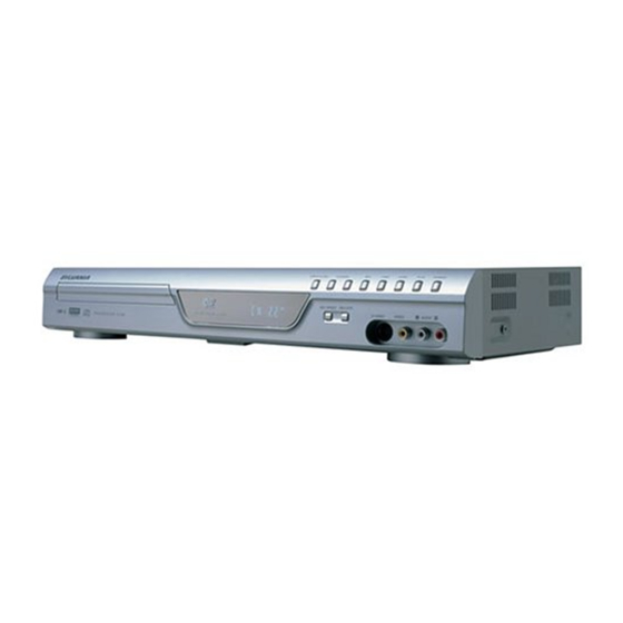
- Page 1 SERVICE MANUAL DVD RECORDER DVR90DG OPEN/CLOSE CHANNEL STOP PLAY POWER REC SPEED REC/OTR S-VIDEO VIDEO AUDIO...
-
Page 2: Table Of Contents
IMPORTANT SAFETY NOTICE Proper service and repair is important to the safe, reliable operation of all Funai Equipment. The service procedures recommended by Funai and described in this service manual are effective methods of performing service operations. Some of these service special tools should be used when and as recommended. -
Page 3: Specifications
SPECIFICATIONS Item Conditions Unit Nominal Limit 1. VIDEO 75 Ω load 1-1. Video Output Vp-p 1-2. S-Video Output 75 Ω load Y (Luminance) Vp-p 75 Ω load C (Chrominance) Vp-p 0.286 1-3. Component Output 75 Ω load Y (Luminance) Vp-p 75 Ω... -
Page 4: Laser Beam Safety Precautions
LASER BEAM SAFETY PRECAUTIONS This DVD player uses a pickup that emits a laser beam. Do not look directly at the laser beam coming from the pickup or allow it to strike against your skin. The laser beam is emitted from the location shown in the figure. When checking the laser diode, be sure to keep your eyes at least 30 cm away from the pickup lens when the diode is turned on. -
Page 5: Important Safety Precautions
IMPORTANT SAFETY PRECAUTIONS Product Safety Notice Also check areas surrounding repaired locations. J. Be careful that foreign objects (screws, solder Some electrical and mechanical parts have special droplets, etc.) do not remain inside the set. safety-related characteristics which are often not K. - Page 6 Safety Check after Servicing Examine the area surrounding the repaired location for damage or deterioration. Observe that screws, parts, and wires have been returned to their original positions. Afterwards, do the following tests and confirm the specified values to verify compliance with safety standards. 1.
-
Page 7: Standard Notes For Servicing
STANDARD NOTES FOR SERVICING Circuit Board Indications Pb (Lead) Free Solder 1. The output pin of the 3 pin Regulator ICs is When soldering, be sure to use the Pb free solder. indicated as shown. How to Remove / Install Flat Pack-IC Top View Bottom View 1. - Page 8 3. The flat pack-IC on the CBA is affixed with glue, so With Soldering Iron: be careful not to break or damage the foil of each 1. Using desoldering braid, remove the solder from pin or the solder lands under the IC when all pins of the flat pack-IC.
- Page 9 2. Installation With Iron Wire: 1. Using desoldering braid, remove the solder from 1. Using desoldering braid, remove the solder from all pins of the flat pack-IC. When you use solder the foil of each pin of the flat pack-IC on the CBA flux which is applied to all pins of the flat pack-IC, so you can install a replacement flat pack-IC more you can remove it easily.
- Page 10 Instructions for Handling Semi- conductors Electrostatic breakdown of the semi-conductors may occur due to a potential difference caused by electrostatic charge during unpacking or repair work. 1. Ground for Human Body Be sure to wear a grounding band (1 MΩ) that is properly grounded to remove any static electricity that may be charged on the body.
-
Page 11: Cabinet Disassembly Instructions
CABINET DISASSEMBLY INSTRUCTIONS 1. Disassembly Flowchart Note: (1) Identification (location) No. of parts in the figures This flowchart indicates the disassembly steps to gain (2) Name of the part access to item(s) to be serviced. When reassembling, (3) Figure Number for reference follow the steps in reverse order. - Page 12 (S-4) Desolder (L-1) [4] SW CBA [5] PCB Holder S Earth (L-1) (S-3) Plate (L-1) (L-2) [2] Front Assembly Fig. D2 Fig. D4 (S-2) (S-2) [3] DVD Mechanism & DVD Main (S-7) CBA Assembly (S-7) CN101 Heat Sink Earth Plate CN701 Main Sheet [7] AV CBA...
- Page 13 3. How to Eject Manually Note: When rotating the gear, be careful not to damage the gear. 1. Remove the Top Cover. 2. Rotate the gear in the direction of the arrow manually as shown below until the tray descends. 3.
-
Page 14: How To Initialize The Dvd Recorder
HOW TO INITIALIZE THE DVD RECORDER To put the program back at the factory-default, initialize the DVD recorder as the following procedure. 1. Turn the DVD recorder on. 2. Confirm that no disc is loaded or that the disc tray is open. -
Page 15: Firmware Renewal Mode
FIRMWARE RENEWAL MODE 1. Turn the power on and remove the disc on the tray. 4. Select the firmware version pressing arrow buttons, then press [ENTER]. 2. To put the DVD recorder into version up mode, Fig. d appears on the screen and Fig. e appears press [CM SKIP], [6], [5], and [4] buttons on the on the VFD. -
Page 16: Function Indicator Symbols
FUNCTION INDICATOR SYMBOLS Note: If an error occurs, a message with the error number appears on the screen. Recording Error Error message You cannot record on this disc as Power Calibration Area is full. Error No. Error Message Solution Error Description Priority An error occurs during data reading. - Page 17 Error Message Solution Error Description Priority This program is not recordable Set “DVD-RW Recording During the CGMS picture (possible to in Video mode. Format” to “VR mode”. record once) input. (Video Format Disc) During the CGMS picture (possible to This program is not allowed to Insert a ver.1.1 CPRM record once) input.
-
Page 18: Block Diagrams
BLOCK DIAGRAMS System Control Block Diagram 1-9-1 E7A00BLS... - Page 19 Digital Signal Process Block Diagram 1-9-2 E7A00BLD...
- Page 20 Video Block Diagram 1-9-3 E7A00BLV...
- Page 21 Audio Block Diagram 1-9-4 E7A00BLA...
- Page 22 Power Supply Block Diagram 1-9-5 E7A00BLP...
-
Page 23: Schematic Diagrams / Cba's And Test Points
SCHEMATIC DIAGRAMS / CBA’S AND TEST POINTS Standard Notes WARNING Many electrical and mechanical parts in this chassis have special characteristics. These characteristics often pass unnoticed and the protection afforded by them cannot necessarily be obtained by using replacement components rated for higher voltage, wattage, etc. - Page 24 LIST OF CAUTION, NOTES, AND SYMBOLS USED IN THE SCHEMATIC DIAGRAMS ON THE FOLLOWING PAGES: 1. CAUTION: FOR CONTINUED PROTECTION AGAINST FIRE HAZARD, REPLACE ONLY WITH THE SAME TYPE FUSE. ATTENTION: POUR UNE PROTECTION CONTINUE LES RISQES D'INCELE N'UTILISER QUE DES FUSIBLE DE MÊME TYPE. RISK OF FIRE-REPLACE FUSE AS MARKED.
- Page 25 DVD Main 1/5 Schematic Diagram NOTE: 1. The order of pins shown in this diagram is different from that of actual IC101. 2. IC101 is divided into five and shown as IC101 (1/5) ~ IC101 (5/5) in this DVD Main Schematic Diagram Section. DVD MAIN 1/5 Ref No.
- Page 26 DVD Main 2/5 Schematic Diagram NOTE: 1. The order of pins shown in this diagram is different from that of actual IC101. 2. IC101 is divided into five and shown as IC101 (1/5) ~ IC101 (5/5) in this DVD Main Schematic Diagram Section. DVD MAIN 2/5 Ref No.
- Page 27 DVD Main 3/5 Schematic Diagram NOTE: 1. The order of pins shown in this diagram is different from that of actual IC101. 2. IC101 is divided into five and shown as IC101 (1/5) ~ IC101 (5/5) in this DVD Main Schematic Diagram Section. DVD MAIN 3/5 Ref No.
- Page 28 DVD Main 4/5 Schematic Diagram NOTE: 1. The order of pins shown in this diagram is different from that of actual IC101. 2. IC101 is divided into five and shown as IC101 (1/5) ~ IC101 (5/5) in this DVD Main Schematic Diagram Section. DVD MAIN 4/5 Ref No.
- Page 29 DVD Main 5/5 Schematic Diagram NOTE: 1. The order of pins shown in this diagram is different from that of actual IC101. 2. IC101 is divided into five and shown as IC101 (1/5) ~ IC101 (5/5) in this DVD Main Schematic Diagram Section. DVD MAIN 5/5 Ref No.
- Page 30 AV 1/5 Schematic Diagram *1 NOTE These components (IC1502, C1509) can be used in any models. However, you cannot mix components under Group A with the ones under Group B. You can choose either Group. The difference between Group A and Group B is shown below. Group A Group B BU4219G-TR...
- Page 31 AV 2/5 Schematic Diagram AV 2/5 Ref No. Position IC1101 IC1102 IC1301 IC1701 TRANSISTORS Q1101 Q1102 Q1303 Q1304 CONNECTOR CN1101 1-10-9 E7A00SCAV2...
- Page 32 AV 3/5 Schematic Diagram AV 3/5 Ref No. Position IC1201 IC1401 TRANSISTORS Q1161 Q1201 Q1202 Q1203 Q1241 E7A00SCAV3 1-10-10...
- Page 33 AV 4/5 Schematic Diagram CAUTION ! For continued protection against fire hazard, CAUTION ! replace only with the same type fuse. Fixed voltage (or Auto voltage selectable) power supply circuit is used in this unit. NOTE: ATTENTION : Pour une protection continue les risqes The voltage for parts in hot circuit is measured using If Main Fuse (F1001) is blown , check to see that all components in the power supply d'Incele n'utiliser que des fusible de même type.
- Page 34 AV 5/5 Schematic Diagram FL2001 MATRIX CHART P.SCAN VCD VCR REPEAT VCD VCR XP SP LP EP REPEAT P.SCAN E7A00SCAV5 1-10-12...
- Page 35 SW Schematic Diagram E7A00SCSW 1-10-13...
- Page 36 AV CBA Top View CAUTION ! Fixed voltage (or Auto voltage selectable) power supply circuit is used in this unit. If Main Fuse (F1001) is blown , check to see that all components in the power supply circuit are not defective before you connect the AC plug to the AC power supply. Otherwise it may cause some components in the power supply circuit to fail.
- Page 37 AV CBA Bottom View CAUTION ! CAUTION ! Fixed voltage (or Auto voltage selectable) power supply circuit is used in this unit. For continued protection against fire hazard, If Main Fuse (F1001) is blown , check to see that all components in the power supply replace only with the same type fuse.
- Page 38 SW CBA Top View SW CBA Bottom View BE7A00F01021B 1-10-16...
-
Page 39: Waveforms
WAVEFORMS Pin 24 of CN1101 Pin 26 of CN1101 VIDEO-Y 0.2V 20µsec VIDEO-Cr 0.2V 20µsec Pin 22 of CN1101 Pin 14 of CN1101 VIDEO-C 0.2V 20µsec AUDIO(L)-OUT 0.5ms C1418 PLUS LEAD Pin 28 of CN1051 VIDEO-CVBS 0.5V 20µsec SPDIF 0.1µsec Pin 28 of CN1101 NOTE: Input: COLOR BAR SIGNAL... -
Page 40: Wiring Diagram
WIRING DIAGRAM E7A00WI 1-12-1... -
Page 41: System Control Timing Charts
SYSTEM CONTROL TIMING CHARTS [ Tray Open ] Power on Push Close button is pressed. Tray insertion INNER-SW Case 3 open? [ open ] button is pressed. Is Timer Case 1 Is slit S5 ET3 passed? passed? Rezero 1 Rezero 2 Is Timer Case 4 ET1 passed? - Page 42 Parameter S*: Encoder pulse ET*: Error V*: Voltage (HEX) T*: Event timer (HEX) detection timer V0: 2.0 V (00d) S1: 300 (12c) T1: 0.1 s ET1: 5.0 s V1: 4.5 V (022) S2: 3300 (ce4) T2: 3.0 s ET2: 5.0 s V2: 2.2 V (010) S3: 3935 (f5f) T3: 3.0 s...
- Page 43 Tray close Tray ejection direction SLED Tray insersion direction open INNER-SW close Timer Push close Push Close Encoder pulse SLED Tray insersion direction open INNER-SW close Timer 1-13-3 R2NTI...
- Page 44 Case 1 SLED Tray insersion direction open INNER-SW close Timer Rezero 1 Case 2 Tray ejection direction SLED Tray insersion direction open INNER-SW close Rezero 2 Case 3 (When [OPEN] button is pressed before the S5 passage.) Encoder pulse Tray ejection direction SLED Timer Case 4 (When [OPEN] button is pressed after the S5 passage.)
- Page 45 Case 5 (Retry.) Tray ejection direction SLED Tray insersion direction open INNER-SW close Start retry. Retry frequency 1st time retry 2nd time retry 3rd time retry 4th time retry 5th time retry 6th time retry 1-13-5 R2NTI...
-
Page 46: Ic Pin Function Descriptions
IC PIN FUNCTION DESCRIPTIONS IC1501 (SUB MICRO CONTROLLER) Signal Function Name Signal Function Name Serial Data IN KEY-1 Key Data Input 1 34 OUT SCL Serial Clock IN KEY-2 Key Data Input 2 Not Used IN POW-SW Abnormal Voltage Detection Not Used IN AFT Tuner Voltage Input Signal... - Page 47 IC2001 (VFD DRIVER) Signal Function Name IN CLK Serial Clock IN STB Serial Interface Strobe Not Used Not Used Power Supply Segment Output Pull Down Level 16 OUT i Segment Output Grid Output Power Supply IN OSC Oscillator Input Not Used IN DIN Serial Data Input 1-14-2...
-
Page 48: Lead Identifications
LEAD IDENTIFICATIONS KTC3203-Y-AT/P KTA1267Y-AT/P UTC4558 PQ070XF01SZH KTC3205-Y-AT/P KTA1271-Y-AT/P 2SA966(Y) KTC3199-GR-AT/P KRC103M-AT/P 1 2 3 4 E C B E C B KIA4558P/P PT6313-S-TP(L) 2SK3757(Q) MM1697AJBE G D S MN101C77AFK1 CD4052BPWR BU4219G-TR S2Y52 R3112N191A-TR-FA PST3619NR 1 2 3 E C B Note: PS2561A-1(Q) MM1637XVBE... -
Page 49: Exploded Views
EXPLODED VIEWS Cabinet 2L021 See Electrical Parts List for parts with this mark. 2L021 Some Ref. Numbers are not in sequence. 2L021 DVD Mechanism & DVD Main CBA Assembly 2L031 2L021 2L031 2L081 2L012 SW CBA 2L021 2L081 2L081 2L081 2B10 AV CBA 1-16-1... - Page 50 Packing Some Ref. Numbers are not in sequence. Unit 1-16-2 E7A00PEX...
-
Page 51: Mechanical Parts List
MECHANICAL PARTS LIST PRODUCT SAFETY NOTE: Products marked with a # have special characteristics important to safety. Before replacing any of these components, read carefully the product safety notice in this service manual. Don't degrade the safety of the product through improper servicing. -
Page 52: Electrical Parts List
ELECTRICAL PARTS LIST PRODUCT SAFETY NOTE: Products marked with a Ref. No. Description Part No. # have special characteristics important to safety. C1065 CHIP CERAMIC CAP .(1608) B K 0.033µF/ 50V CHD1JK30B333 Before replacing any of these components, read C1066 CERAMIC CAP . - Page 53 Ref. No. Description Part No. Ref. No. Description Part No. C1337 CHIP CERAMIC CAP .(1608) F Z 0.1µF/ 50V CHD1JZ30F104 C1729 ELECTROLYTIC CAP . 2.2µF/ 50V M CE1JMASDL2R2 C1338 ELECTROLYTIC CAP . 100µF/ 6.3V M NP CP0KMASNC101 C1730 CHIP CERAMIC CAP .(1608) B K 0.033µF/ 50V CHD1JK30B333 C1405 CHIP CERAMIC CAP .(1608) B K 0.01µF/ 50V...
- Page 54 Ref. No. Description Part No. Ref. No. Description Part No. CARBON RES. 1/4W J 100k Ω If IC1502is BU4219G-TR, R3112N191A-TR-FA , then C1225 is 0.015µF. R1011 RCX4JATZ0104 CARBON RES. 1/4W J 1k Ω IC1502 VOLTAGE DETECT R3112N191A-TR-FA or QSZBA0TRC021 R1012 RCX4JATZ0102 CARBON RES.
- Page 55 Ref. No. Description Part No. Ref. No. Description Part No. CHIP RES. 1/10W J 110 Ω CHIP RES. 1/10W J 470 Ω R1151 RRXAJR5Z0111 R1507 RRXAJR5Z0471 CHIP RES.(1608) 1/10W 0 Ω CHIP RES.(1608) 1/10W 0 Ω R1152 RRXAZR5Z0000 R1508 RRXAZR5Z0000 CHIP RES.
- Page 56 Ref. No. Description Part No. Ref. No. Description Part No. FL2001 VACUUM FLUORESCENT DISPLAY 7-BT-301N TVFD1C0FT048 SWITCHES FH1001 FUSE HOLDER MSF-015 LF (B110) XH01Z00LY002 SW3001 TACT SWITCH SKQSAB SST0101AL038 FH1002 FUSE HOLDER MSF-015 LF (B110) XH01Z00LY002 SW3002 TACT SWITCH SKQSAB SST0101AL038 JK2101 S TYPE JACK DIN-405...
- Page 57 DVR90DG E7A00UD 2006-1-10...
Need help?
Do you have a question about the DVR90DG and is the answer not in the manual?
Questions and answers