Table of Contents
Advertisement
Quick Links
Advertisement
Table of Contents

Related Manuals for Sylvania Durabrand DVR900E


Summary of Contents for Sylvania Durabrand DVR900E
- Page 1 SERVICE MANUAL DVD RECORDER DVR900E...
-
Page 2: Table Of Contents
IMPORTANT SAFETY NOTICE Proper service and repair is important to the safe, reliable operation of all Funai Equipment. The service procedures recommended by Funai and described in this service manual are effective methods of performing service operations. Some of these service special tools should be used when and as recommended. -
Page 3: Specifications
SPECIFICATIONS ITEM CONDITIONS UNIT NOMINAL LIMIT 1. VIDEO 1-1. Video Output 75 ohm load Vp-p 1-2. S-Video Output Y (Luminance) 75 ohm load Vp-p C (Chrominance) 75 ohm load Vp-p 0.286 1-3. Component Output Y (Luminance) 75 ohm load Vp-p Cb (Chrominance) 75 ohm load Vp-p... -
Page 4: Laser Beam Safety Precautions
LASER BEAM SAFETY PRECAUTIONS This DVD player uses a pickup that emits a laser beam. Do not look directly at the laser beam coming from the pickup or allow it to strike against your skin. The laser beam is emitted from the location shown in the figure. When checking the laser diode, be sure to keep your eyes at least 30cm away from the pickup lens when the diode is turned on. -
Page 5: Important Safety Precautions
IMPORTANT SAFETY PRECAUTIONS Product Safety Notice I. Also check areas surrounding repaired locations. J. Be careful that foreign objects (screws, solder Some electrical and mechanical parts have special droplets, etc.) do not remain inside the set. safety-related characteristics which are often not evi- K. - Page 6 Safety Check after Servicing Examine the area surrounding the repaired location for damage or deterioration. Observe that screws, parts, Chassis or Secondary Conductor and wires have been returned to their original posi- tions. Afterwards, do the following tests and confirm the specified values to verify compliance with safety Primary Circuit Terminals standards.
-
Page 7: Standard Notes For Servicing
STANDARD NOTES FOR SERVICING Circuit Board Indications Pb (Lead) Free Solder When soldering, be sure to use the Pb free solder. 1. The output pin of the 3 pin Regulator ICs is indi- cated as shown. How to Remove / Install Flat Pack-IC Top View Bottom View 1. - Page 8 3. The flat pack-IC on the CBA is affixed with glue, so With Soldering Iron: be careful not to break or damage the foil of each (1) Using desoldering braid, remove the solder from all pin or the solder lands under the IC when removing pins of the flat pack-IC.
- Page 9 2. Installation With Iron Wire: (1) Using desoldering braid, remove the solder from all (1) Using desoldering braid, remove the solder from pins of the flat pack-IC. When you use solder flux the foil of each pin of the flat pack-IC on the CBA so which is applied to all pins of the flat pack-IC, you you can install a replacement flat pack-IC more can remove it easily.
- Page 10 Instructions for Handling Semi-conductors Electrostatic breakdown of the semi-conductors may occur due to a potential difference caused by electro- static charge during unpacking or repair work. 1. Ground for Human Body Be sure to wear a grounding band (1MΩ) that is prop- erly grounded to remove any static electricity that may be charged on the body.
-
Page 11: Operating Controls And Functions
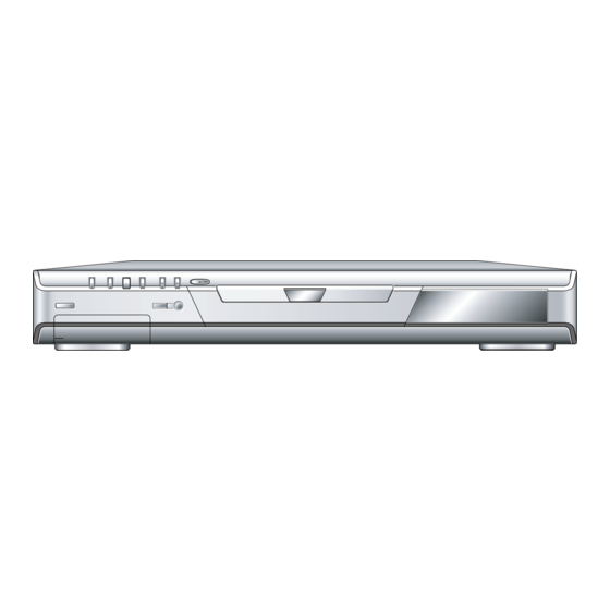
OPERATING CONTROLS AND FUNCTIONS 1-5-1 E6502IB... - Page 12 1-5-2 E6502IB...
-
Page 13: Cabinet Disassembly Instructions
CABINET DISASSEMBLY INSTRUCTIONS 1. Disassembly Flowchart (1): Identification (location) No. of parts in the figures (2): Name of the part This flowchart indicates the disassembly steps to gain (3): Figure Number for reference access to item(s) to be serviced. When reassembling, (4): Identification of parts to be removed, unhooked, follow the steps in reverse order. - Page 14 [5] DVD BE Main CBA Unit CN4203 (S-5) (S-5) [3] SW CBA BE Earth Spring (S-2) [7] DC Fan Motor (S-6) (S-6) (L-1) Fan Holder (S-2) [6] Holder D (L-1) (S-7) (L-2) (L-1) CN2203 [2] Front Assembly Fig. D2 Fig. D4 (S-3) Fan Sheet (S-4)
- Page 15 (S-7) (S-7) (W-1) (S-7) [10] Jack CBA (S-9) (S-10) [8] AV CBA Lead with Lead with red stripe red stripe [9] FL CBA (S-8) Desolder Desolder Fig. D5 HOW TO EJECT MANUALLY 1. Remove the Top Cover. 2. Remove the Front Assembly. 3.
-
Page 16: How To Initialize The Dvd Recorder
HOW TO INITIALIZE THE DVD RECORDER To put the program back at the factory-default, initialize the DVD recorder as the following procedure. 1. Turn the DVD recorder on. 2. Confirm that no disc is loaded or that the disc tray is open. -
Page 17: Block Diagrams
BLOCK DIAGRAMS System Control Block Diagram 1-7-1 E6502BLS... - Page 18 Digital Signal Process Block Diagram 1-7-2 E6502BLD...
- Page 19 Video Block Diagram 1-7-3 E6502BLV...
- Page 20 Audio Block Diagram E6502BLA 1-7-4...
- Page 21 Power Supply Block Diagram 1-7-5 E6502BLP...
-
Page 22: Function Indicator Symbols
FUNCTION INDICATOR SYMBOLS Note: If an error occurs, a message with the error number appears on the screen. Recording Error Error message You cannot record on the disc as Power Calibration Area is full. Error No. Error Message Solution Error Description Priority An error occurs during data reading. - Page 23 Error Message Solution Error Description Priority This program is not recordable Set "DVD-RW Recording During the CGMS picture (possible a in Video mode. Format" to "VR mode". record once) input. (Video Format Disc) During the CGMS picture (possible a This program is not allowed to Insert a ver.1.1 CPRM record once) input.
-
Page 24: Schematic Diagrams / Cba's And Test Points
SCHEMATIC DIAGRAMS / CBA’S AND TEST POINTS Standard Notes WARNING Many electrical and mechanical parts in this chassis have special characteristics. These characteristics often pass unnoticed and the protection afforded by them cannot necessarily be obtained by using replace- ment components rated for higher voltage, wattage, etc. - Page 25 LIST OF CAUTION, NOTES, AND SYMBOLS USED IN THE SCHEMATIC DIAGRAMS ON THE FOLLOWING PAGES: 1. CAUTION: FOR CONTINUED PROTECTION AGAINST FIRE HAZARD, REPLACE ONLY WITH THE SAME TYPE FUSE. ATTENTION: POUR UNE PROTECTION CONTINUE LES RISQES D'INCELE N'UTILISER QUE DES FUSIBLE DE MÊME TYPE.
- Page 26 DVD FE Main 1/4 Schematic Diagram REC Video+Audio Signal (Digital) PB Video+Audio Signal (Digital) DVD FE MAIN 1/4 Ref No. Position IC5101 IC5103 IC5202 TRANSISTORS Q5101 Q5201 CONNECTOR CN5101 E6502SCFM1 1-8-3 1-8-4...
- Page 27 DVD FE Main 2/4 Schematic Diagram REC Video+Audio Signal (Digital) PB Video+Audio Signal (Digital) DVD FE MAIN 2/4 Ref No. Position IC5301 IC5804 TRANSISTORS Q5301 Q5302 Q5802 CONNECTOR CN5301 1-8-5 1-8-6 E6502SCFM2...
- Page 28 DVD FE Main 3/4 Schematic Diagram DVD FE MAIN 3/4 Ref No. Position IC5401 IC5501 IC5503 IC5601 IC5805 IC5806 CONNECTORS CN5501 CN5502B CN5603 CN5603B CN5801 1-8-7 1-8-8 E6502SCFM3...
- Page 29 DVD FE Main 4/4 Schematic Diagram DVD FE MAIN 4/4 Ref No. Position IC5701 IC5703 IC5704 IC5705 IC5706 IC5707 CONNECTORS CN5701 CN5602B E6502SCFM4 1-8-9 1-8-10...
- Page 30 DVD BE Main 1/4 Schematic Diagram REC Video+Audio Signal (Digital) PB Video+Audio Signal (Digital) *1 Note: REC Video Signal (Digital) REC Audio Signal (Analog) PB Video Signal (Digital) PB Audio Signal 1. The order of pins shown are different from that of IC3 itself. REC Audio Signal (Digital) PB Audio Signal (Digital) 2.
- Page 31 DVD BE Main 2/4 Schematic Diagram *1 Note: 1. The order of pins shown are different from that of IC3 itself. 2. IC3 is shown as IC3(1/6) through IC3(6/6) in DVD BE Main Schematic Diagram section. DVD BE MAIN 2/4 Ref No.
- Page 32 DVD BE Main 3/4 Schematic Diagram *1 Note: 1. The order of pins shown are different from that of IC3 itself. 2. IC3 is shown as IC3(1/6) through IC3(6/6) in DVD BE Main Schematic Diagram section. DVD BE MAIN 3/4 Ref No.
- Page 33 DVD BE Main 4/4 Schematic Diagram *1 Note: REC Video+Audio Signal (Digital) PB Video+Audio Signal (Digital) 1. The order of pins shown are different from that of IC3 itself. 2. IC3 is shown as IC3(1/6) through IC3(6/6) in DVD BE Main Schematic Diagram section. DVD BE MAIN 4/4 Ref No.
- Page 34 AV 1/4 Schematic Diagram AV 1/4 Ref No. Position IC4201 IC4202 TRANSISTORS Q4261 Q4262 CONNECTORS CN2204 CN4202 CN4203 E6502SCAV1 1-8-19 1-8-20...
- Page 35 AV 2/4 Schematic Diagram REC Video Signal (Analog) PB Video Signal REC Audio Signal (Analog) PB Audio Signal AV 2/4 Ref No. Position IC4041 IC4163 IC4164 IC4165 IC4166 TRANSISTORS Q4161 Q4162 Q4502 Q4505 CONNECTOR CN4101 CN4401 E6502SCAV2 1-8-21 1-8-22...
- Page 36 AV 3/4 Schematic Diagram REC Video Signal (Analog) PB Video Signal REC Audio Signal (Analog) PB Audio Signal REC Audio Signal (Digital) PB Audio Signal (Digital) AV 3/4 Ref No. Position IC4401 IC4421 TRANSISTORS Q4301 Q4424 Q4425 Q4426 Q4451 E6502SCAV3 1-8-23 1-8-24...
- Page 37 AV 4/4 Schematic Diagram CAUTION ! CAUTION Fixed voltage ( or Auto voltage selectable ) power supply circuit is used in this unit. FOR CONTINUED PROTECTION AGAINST FIRE HAZARD, If Main Fuse (F2101) is blown, check to see that all components in the power supply REPLACE ONLY WITH THE SAME TYPE FUSE.
- Page 38 FL Schematic Diagram FL2301 MATRIX CHART P.SCAN VCD VCR REPEAT VCD VCR XP SP LP EP REPEAT P.SCAN Ref No. Position IC2301 CONNECTOR CN2301 1-8-27 1-8-28 E6502SCFL...
- Page 39 Jack Schematic Diagram SW Schematic Diagram REC Video Signal (Analog) REC Audio Signal (Analog) E6502SCSW E6502SCJK 1-8-29 1-8-30...
- Page 40 AV CBA Top View CAUTION ! NOTE : Fixed voltage ( or Auto voltage selectable ) power supply circuit is used in this unit. The voltage for parts in hot circuit is measured If Main Fuse (F2101) is blown, check to see that all components in the power supply using hot GND as a common terminal.
- Page 41 AV CBA Bottom View CAUTION ! NOTE : Fixed voltage ( or Auto voltage selectable ) power supply circuit is used in this unit. The voltage for parts in hot circuit is measured If Main Fuse (F2101) is blown, check to see that all components in the power supply using hot GND as a common terminal.
- Page 42 FL CBA Top View Jack CBA Top View FL CBA Bottom View Jack CBA Bottom View BE6500F01023D BE6500F01023B 1-8-35 1-8-36...
- Page 43 SW CBA Top View SW CBA Bottom View BE6500F01023C 1-8-37 1-8-38...
-
Page 44: Waveforms
WAVEFORMS Pin 12 of CN4401 Pin 8 of CN4401 VIDEO-Y 0.2V 20µsec VIDEO-Cr 0.2V 20µsec Pin 14 of CN4401 Pin 25 of CN4401 VIDEO-C 0.2V 20µsec A-OUT(L) 0.1µsec C4411 PLUS LEAD Pin 18 of CN4502 VIDEO-CVBS 0.5V 20µsec SPDIF 0.1µsec Pin 10 of CN4401 NOTE: Input: COLOR BAR SIGNAL... -
Page 45: Wiring Diagram
WIRING DIAGRAM E6502WI 1-10-1... -
Page 46: Firmware Renewal Mode
FIRMWARE RENEWAL MODE 1. Turn the power on and remove the disc on the tray. 4. Select the firmware version using arrow buttons, 2. To put the DVD recorder into version up mode, then press [ENTER]. press [CM SKIP], [6], [5], and [4] buttons on the Fig. -
Page 47: System Control Timing Charts
SYSTEM CONTROL TIMING CHARTS Tray in 5.0V Tray in 5.0V Tray out 1.35V Sled Drive 1.35V Disc Drive 1.35V Focus Drive 1.35V Tracking Drive Tray out 5.0V Tray in 5.0V Tray out Sled Drive 1.35V Disc Drive 1.35V 1.35V Focus Drive 1.35V Tracking Drive 1-12-1... - Page 48 Spin up 5.0V Tray in 5.0V Tray out Sled Drive 1.35V Disc Drive 1.35V 1.35V Focus Drive 1.35V Tracking Drive Playing 5.0V Tray in 5.0V Tray out Sled Drive 1.35V Disc Drive 1.35V 1.35V Focus Drive 1.35V Tracking Drive 1-12-2 E6TI...
-
Page 49: Ic Pin Function Descriptions
IC PIN FUNCTION DESCRIPTIONS IC4201 [ SUB MICRO CONTROLLER ] Signal Name Function Name Signal Name Function N.U. Not Used Name KEY-1 Key Data Input 1 N.U. Not Used KEY-2 Key Data Input 2 N.U. Not Used N.U. Not Used N.U. - Page 50 IC2301 [ PT6313-S-TP ] Signal Name Function Name Signal Name Function AVSS Ground Name Serial Clock N.U. Not Used REG- Serial Interface Strobe Power Regurator Control CONT Signal N.U. Not Used Tuner Voltage Input Signal N.U. Not Used Aspect Ratio Detector SDET-1 Signal Power Supply...
-
Page 51: Lead Identifications
LEAD IDENTIFICATIONS PQ070XF01SZ 2SC2785(H) 2SC2120-Y(TPE2) KTA1267(Y) KTC3203(Y) KTC3199(GR,BL) 1 2 3 4 E C B E C B 2SK3757(Q) NJM4558D PT6313-S-TP MM1657XJBE NJM2100D SC16313 G D S M38039MC-177HP CD4052BPWR S2Y52 MM1637XVBE E C B Note: AN5832SA-E1 A: Anode PS2561A-1(W) PST597INR K: Cathode PS2561A-1(Q) E: Emitter... -
Page 52: Exploded Views
EXPLODED VIEWS Cabinet See Electrical Parts List 2L021 for parts with this mark. 2L021 Some Ref. Numbers are not in sequence. 2L011 SW CBA 2L021 2L063 AC2101 2L081 2L081 2L081 DVD BE Main 2L071 CBA Unit 2L071 2L031 2L031 F2101 2L042 AV CBA 2B10... - Page 53 Packing Some Ref. Numbers are not in sequence. 2B12 Unit 1-15-2 E6502EX...
-
Page 54: Mechanical Parts List
MECHANICAL PARTS LIST PRODUCT SAFETY NOTE: Products marked with a # Ref. No. Description Part No. have special characteristics important to safety. Before RF CABLE 2.5C-2V or WPZ0901TM002 replacing any of these components, read carefully the RF CABLE DC95M95M001 WPZ0901CAB01 product safety notice in this service manual. -
Page 55: Electrical Parts List
ELECTRICAL PARTS LIST PRODUCT SAFETY NOTE: Products marked with a # Ref. No. Description Part No. have special characteristics important to safety. Before ELECTROLYTIC CAP . 1000µF/6.3V M CE0KMASTL102 replacing any of these components, read carefully the C2205 CERAMIC CAP . B K 220pF/500V CCD2JKP0B221 product safety notice in this service manual. - Page 56 Ref. No. Description Part No. Ref. No. Description Part No. C4058 CHIP CERAMIC CAP .(1608) B K 0.033µF/50V CHD1JK30B333 C4207 CHIP CERAMIC CAP .(1608) CH J 22pF/50V CHD1JJ3CH220 C4059 ELECTROLYTIC CAP . 2.2µF/50V M or CE1JMASDL2R2 C4208 CHIP CERAMIC CAP .(1608) CH J 22pF/50V CHD1JJ3CH220 ELECTROLYTIC CAP .
- Page 57 Ref. No. Description Part No. Ref. No. Description Part No. C4505 ELECTROLYTIC CAP . 100µF/6.3V M or CE0KMASDL101 D2217 SWITCHING DIODE 1SS133(T-77) or QDTZ001SS133 ELECTROLYTIC CAP . 100µF/6.3V M CE0KMASTL101 SWITCHING DIODE 1N4148M NDTZ01N4148M C4506 CHIP CERAMIC CAP .(1608) F Z 0.1µF/50V or CHD1JZ30F104 D2218 ZENER DIODE DZ-6.8BSBT265 or...
- Page 58 Ref. No. Description Part No. Ref. No. Description Part No. METAL OXIDE FILM RES. 1W J 12k Ω L4501 CHOKE COIL 22µH-K LLBD00PKV006 RN01123KE010 CARBON RES. 1/4W J 470k Ω L4502 CHOKE COIL 22µH-K LLBD00PKV006 R2107 RCX4JATZ0474 CARBON RES. 1/4W J 15k Ω TRANSISTORS R2108 RCX4JATZ0153...
- Page 59 Ref. No. Description Part No. Ref. No. Description Part No. CHIP RES.(1608) 1/10W 0 Ω CHIP RES.(1608) 1/10W J 4.7k Ω R4131 RRXAZR5Z0000 R4222 RRXAJR5Z0472 CHIP RES.(1608) 1/10W 0 Ω CHIP RES.(1608) 1/10W J 47k Ω R4134 RRXAZR5Z0000 R4223 RRXAJR5Z0473 CHIP RES.(1608) 1/10W 0 Ω...
- Page 60 Ref. No. Description Part No. Ref. No. Description Part No. CHIP RES.(1608) 1/10W J 75 Ω CHIP RES. 1/10W F 120 Ω R4327 RRXAJR5Z0750 RRXAFR5J1200 CHIP RES.(1608) 1/10W J 75 Ω MISCELLANEOUS R4328 RRXAJR5Z0750 R4330 PCB JUMPER D0.6-P5.0 JW5.0T AC2101# AC CORD PB8K9F9110A-057 or WAC0172LW008 R4331 PCB JUMPER D0.6-P5.0...
- Page 61 Ref. No. Description Part No. Ref. No. Description Part No. CHIP RES.(1608) 1/10W J 360 Ω R3009 RRXAJR5Z0361 RE2301 REMOTE RECEIVER MIM-93M6DKF or USESJRSUNT01 CHIP RES.(1608) 1/10W J 300 Ω R3010 RRXAJR5Z0301 REMOTE RECEIVER PIC-37042LU USESJRSKK033 CHIP RES.(1608) 1/10W J 620 Ω R3011 RRXAJR5Z0621 CHIP RES.(1608) 1/10W J 1k Ω...
- Page 62 DVR900E E6502CD 2004-07-05...
Need help?
Do you have a question about the Durabrand DVR900E and is the answer not in the manual?
Questions and answers