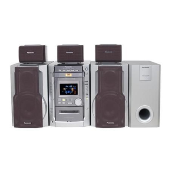
Panasonic SA-DK20 Service Manual
Hide thumbs
Also See for SA-DK20:
- Operating instructions manual (64 pages) ,
- Quick manual (2 pages) ,
- Operating instructions manual (64 pages)
Table of Contents
Advertisement
Specifications
AMPLIFIER SECTION
Power Output
THD 10%, both channels driven
75 Hz
Subwoofer
1 kHz
Front
Center
Surround
Total power in stereo mode
(Front and Subwoofer)
Total power in Home Theater mode
Power output
THD 10%, both channels driven
50 Hz - 120 Hz
Subwoofer
60 Hz - 16 kHz
Front
100 Hz - 16 kHz
Center
Surround
Total power in stereo mode (10% THD)
(Front and Subwoofer)
Total power in Home Theater mode
SA-DK20
Colour
(S)... Silver Type
Area
(P)... U.S.A.
(PC)... Canada
TAPE SECTION :
AR2 MECHANISM SERIES
CD SECTION :
RAE1181Z-S TRAVERSE DECK SERIES
(10% THD)
Input sensitivity
AUX
Input Impedance
150 W (4 Ω)
AUX
FM TUNER SECTION
35 W per ch (6 Ω)
Frequency range
60 W (8 Ω)
30 W per ch (8 Ω)
Sensitivity
S/N 26 dB
220 W
Antenna terminal(s)
AM TUNER SECTION
340 W
Frequency range
Sensitivity
S/N 20 dB (at 1000 kHz)
CASSETTE DECK SECTION
130 W (4 Ω)
Track system
Heads
28 W per ch (6 Ω)
Record/playback
Erasure
44 W (8 Ω)
Motor
25 W per ch (8 Ω)
Recording system
Erasing system
186 W
Tape speed
ORDER NO. MD0203054C1
DVD Stereo System
87.9 - 107.9 MHz (200 kHz steps)
87.5 - 108.0 MHz (100 kHz steps)
520 - 1710 kHz (10 kHz steps)
Double gap ferrite head
© 2002 Matsushita Electronics (S) Pte. Ltd. All rights
reserved. Unauthorized copying and distribution is a
violation of law.
A6
280 W
250 mV
10 kΩ
1.8 µV (IHF)
1.5 µV
75 Ω (unbalanced)
500 µV/m
4 track, 2 channel
Solid permalloy head
DC servo motor
AC bias 100 kHz
AC erase 100 kHz
4.8 cm/s (1 7/8 ips)
Advertisement
Table of Contents

Related Manuals for Panasonic SA-DK20


Summary of Contents for Panasonic SA-DK20
- Page 1 ORDER NO. MD0203054C1 DVD Stereo System SA-DK20 Colour (S)... Silver Type Area (P)... U.S.A. (PC)... Canada TAPE SECTION : AR2 MECHANISM SERIES CD SECTION : RAE1181Z-S TRAVERSE DECK SERIES Specifications AMPLIFIER SECTION (10% THD) 280 W Power Output Input sensitivity...
-
Page 2: Table Of Contents
Mass (7.8 kg) 17.2 lb (One layer per side) Video CD/CD 8 cm/12 cm SYSTEM Video SC-DK20(P) Music Center: SA-DK20(P) Signal system NTSC Front Speaker: SB-DK20(P) Output level Surround Speaker: SB-PT93(P1) 1 Vp-p (75 Ω) Composite video Sub woofer: SB-W20(P) 1 Vp-p (75 Ω) -
Page 3: Safety Precaution
SA-DK20 1 Safety Precaution (This “Safety Precaution” is applied only in U.S.A.) 1. Before servicing, unplug the power cord to prevent an electric shock. 2. When replacing parts, use only manufacturer’s recommended components for safety. 3. Check the condition of the power cord. Replace if wear or damage is evident. -
Page 4: Accessories
SA-DK20 4 Accessories Remote Control Transmitter FM indoor antenna AC mains lead AM Loop antenna Video cable... -
Page 5: Handling Precaution For Traverse Deck (Optical Pickup)
SA-DK20 5 Handling Precaution for Traverse Deck (Optical Pickup) The laser diode in the traverse unit (optical pickup) may break down due to static electricity of clothes or human body. Use due caution to electrostatic breakdown when servicing and handling the laser diode. -
Page 6: Operation Procedures
SA-DK20 6 Operation Procedures... - Page 7 SA-DK20...
-
Page 8: Precaution Of Laser Diode
SA-DK20 7 Precaution of Laser Diode CAUTION : This unit utilizes a class 1 laser. Invisible laser radiation is emitted from the optical pickup lens. When the unit is turned on : 1. Do not look directly into the pick up lens. -
Page 9: Self-Diagnostic Function
SA-DK20 8 Self-Diagnostic Function 8.1. Outline • Self-Diagnosis of error conditions on user equipment according to conditions set by the head office. • Occurance of an error condition and results of operations that occured after entering self-diagnostic mode are displayed via the front (FL) display panel. - Page 10 SA-DK20 Step Operating Procedure Micro-controller operation, processing, etc. Clear recorded error content by pressing the [STOP] Recorded error content is cleared and the following is shown on the button for 5 seconds or more while stopped in the self- front display panel:[CLEAR] is displayed for one second followed by diagnostic mode.
- Page 11 SA-DK20 Error Display Error Explanation Cause (IC number, etc.) Disk → IC7001 F010 Specified value is larger than the specified parental value. Disk → IC7001 F020 No TT_SRPT (RLBN is 0) Disk → IC7001 F021 TT_SRP number is 0 Specified value is larger than the TT_SRP number Disk → IC7001 F022 Disk →...
- Page 12 SA-DK20 Error Display Error Explanation Cause (IC number, etc.) System component bug → IC6201 F702 Message Command Changed System component bug → IC6201 F880 Task number not relevant System component bug → IC6201 F890 Attempted to send message while sending to an AV task (mailbox overflow, etc.)
- Page 13 SA-DK20 8.3.2. Special Commands for the DVD Module • When the SELECTOR is set to DVD/CD the commands for the operations below will be sent to the mechanism component micro-controller. • The mechanism component micro-controller relays these commands without alteration to the DVD module.
- Page 14 SA-DK20 Special Operation Command Operation/Display Release/Remarks All Reset While [INITIALIZED] is being displayed from the user (for design service) Model Table initialization operation press [STOP] on the main unit and If NO DISC or ---READ can be confirmed + 0 x 3C [ENTER] on the remote control.
- Page 15 SA-DK20 as [KC 20 0002]. • The DVD Module has functions that support buttons other than [2] [0] [PLAY], so when K objects are being displayed key codes are as below. [0] [1] [2] [3] [4] [5] [6] [7] [8] [9] [>=10] [PLAY] 8.4.
- Page 16 SA-DK20 8.4.4. Insertion Points for ROM Correction Processing • Processing read-outs from EEPROM − RCaccE2PrSUB: Insert after port or control register setting (AC check). It is also necessary for the EEPROM’s power supply to be in power-off (AC positive). • Processing Modifying Program Calls −...
-
Page 17: Disassembly And Main Component Replacement Procedures
SA-DK20 9 Disassembly and Main Component Replacement Procedures “ATTENTION SERVICER” Some chassis components may have sharp edges. Be careful when disassembling and servicing. 1. This section describes procedures for checking the operation of the major printed circuit boards and replacing the main components. - Page 18 SA-DK20 9.1. Checking for the Main and DVD F/E Module (1/2) and (2/2) P.C.B. Step 3 Remove 4 screws. Step 4 Remove 4 connectors. Step 5 Pull out 4 FFCs. • Checking the DVD F/E Module (2/2) P.C.B. as shown Step 1 Remove 3 screws each both side and 5 screws at rear below.
- Page 19 SA-DK20 9.2. Disassembly for DVD/CD changer unit 9.2.1. Disassembly for the disc tray ornament • Follow the (Step 1) - (Step 3) of item 8.1 When opening the disc tray automatically Step 8 Push the open/close button1, so the disc tray will be close.
- Page 20 SA-DK20 Step 3 Release 2 claws, and then remove the disc tray ornament. Step 4 Push the disc tray.
- Page 21 SA-DK20 9.2.2. Disassembly for the DVD/CD changer unit. • Follow the (Step 1) - (Step 3) of item 8.1 • Follow the disassembly instruction for the disc tray ornament . Step 1 Remove 4 screws. Step 2 Pull out 4 FFCs.
- Page 22 SA-DK20 9.3. Disassembly Procedure for each major P.C.B. Checking • Follow the (Step 1) - (Step 7) of item 8.1 • Follow the (Step 1) - (Step 6) of item 8.2 Step 5 Remove the wires at FP2001, FP3202, FP3203, and FP4202.
- Page 23 SA-DK20 • Checking for Power P.C.B. • Replacement of the Power Amplifier IC and Regulator Transistor. Step 1 Follow the procedures in “Checking procedure for each major P.C.B. Step 2 Remove the wires at CN302, CN303 and H603A/W603 and pull out the Main P.C.B..
- Page 24 SA-DK20 9.5. Terminal P.C.B. Step 1 Unscrew the screw. 9.7. Optical Pickup Unit Step 2 Remove the solders. Step 3 Remove the connector. Step 1 Unscrew the screws. Step 2 Remove the spring holders and the springs. Step 3 Pull out the drive shaft and guide shaft.
- Page 25 SA-DK20 1. Do not touch laser diode, actuator and their peripheries. Caution • When using the soldering iron without anti-static feature, 2. Do not use tester to check laser diode. (Laser diode can be damaged easily.) short circuit the flexible cable terminal with a clip before short-circuiting the land.
- Page 26 SA-DK20 9.9. Disassembly and assembly of the Traverse Unit Step 1 Push the lever from position A to B. Step 2 Pull the stopper (black) in the direction of arrow 1 and push the lever in the direction of arrow 2.
- Page 27 SA-DK20 9.10. Disassembly and assembly of the Disc Tray Step 5 Rotate the hexagonal wrench in the direction of arrow (clockwise), and then open the disc tray fully. Step 2 With lifting the claw in the direction of arrow 1, draw the clamp SW P.C.B.
- Page 28 SA-DK20 Step 1 Slide the drive rack fully in the direction of arrow. Step 4 Holding the disc tray manually, rotate the pulley gear in the direction of arrow. Step 5 Rotate the gear 5 or 6 times manually, and then push the disc tray.
-
Page 29: Measurements And Adjustments
SA-DK20 10 Measurements and Adjustments − EVM (Electronic Volmeter) 10.1. Cassette Deck Section − Digital quency counter • Measurement Condition • Test Tape − Reverse-mode selector switch: − Head azimuth adjustment (8 kHz, -20 dB); QZZCFM − Tape edit: NORMAL −... - Page 30 SA-DK20 2. Insert the Normal blank tape (QZZCRA) into DECK 2 and set the unit to “REC” mode ( use “REC/PAUSE” key). 3. Check so that the output frequency is within the standard value. Standard Value: 86 ±8 kHz 10.1.4. Bias Frequency check 1.
-
Page 31: Illustration Of Ics, Transistors And Diodes
SA-DK20 11 Illustration of ICs, Transistors and Diodes C0JBAR000292 (14P) M62444FPE1 LM2940T5M AN8708FHK C1BB00000574 (16P) C2BBFD000307 (42P) C0FBBK000021 (48P) M62457AFPE1 (16P) C2BBFD000308 (42P) MN677533MP (208P) M62456FPE1 (24P) NJU7313AMT2 (30P) No.1 M5218AFPE3 (8P) M5228FPE1 (14P) No.1 KTC2026 C0JBAA000001 AN7326K C0DBAJG00002 M5218AP... -
Page 32: Terminal Function Of Ic's
SA-DK20 12 Terminal Function of IC’s 12.1. IC601 (C2BBGF000359 ) Pin No. Mark Function VREF Reference for A-D System Microprocessor SER7 Searal 7 output (PLL CE) SER6 Searal 6 output (PLL/DSP CK) Pin No. Mark Function SER5 Searal 5 output (PLL/DSP DA) -
Page 33: Block Diagram
SA-DK20 13 Block Diagram IC5201 AN8708FHK FRONT END PROCESSOR OPTICAL PICKUP UNIT Q5215 HIGH FREQUENCY LED DRIVE LPCD2 MODULATOR Q5211 LED DRIVE LD-IN LPCD1 LD-OUT DVD MODULATOR 26,27 FLTOP, FLTON VIN2 TRACKING BALANCE VIN1 TBAL LPC1 VIN8 VIN7 FOCUS BALANCE... - Page 34 SA-DK20 IC2001 MN677203NP1 OPTICAL DISC CONTROLLER LDIN IC2501 SPPOL_GIO3_SPOPC C0GBG0000033 MOTOR DRIVE 47,49 ARF,NARF STEPPING MOTOR UNIT STEPPING MOTOR VO3- CASH UCAS IC2061 M2501 TBAL C3ABKG000057 DRAMWE VO3+ 4M DRAM VO4- M2502 VO4+ 2~5, 18~21, 7~10, 24~28 FBAL 35~38, 40~43...
- Page 35 SA-DK20 IC3001 MN677533MP AV DECORDER JK701 VIDEO OUT IC3061 C3ABMG000103 IC3301 C1AB00001393 VIDEO BUFFER SDRAM C-IN QR3301 WIDE1 SWITCH C-OUT 19~24 2~12 27~32 39~49 CR/R CV-OUT 2~4,6~8,10,201 203,204,206,207 JK701 MA0~11 CV-SAG VIDEO OUT 158~181 MDQ0~15 Y-IN Y-SAG Y-OUT IC4211 C0FBBK000021...
- Page 36 SA-DK20 IC201 NJU7313AMT2 SELECTOR 3(28) IC202 M5218AFPE3 4(27) 6(25) TUNER 5(26) FROM IC601 MODULE 2(30) JK201 AUX1 7(24) DATA Level shift Latch circuit Shift register C0GAM0000005 MOTOR DRIVE OUT1 OUT2 TO DVD BLOCK POWER SUPPLY CONTROL Q451 SWITCH GP1S94 Q452...
- Page 37 SA-DK20 PB HEAD (Lch) FILTER IC1001 FILTER AN7326K P/B REC AMP 21(2) 20(3) 15(8) 22(1) 19(4) 16(7) RIPPLE REJECTION LOGIC SWITCH MUTE REC AMP (L) IC1000 C1AA00000612 ANALOG SWITCH Q1304 SWITCH (REC:H) Q1309, Q1310, L1301 R/P HEAD Q1312 Q1308 BIAS...
- Page 38 SA-DK20 IC206 C0JBAR000292 ANALOG SWITCH 13(1) 14(15) X1(Y1) SL(SR) 12(2) X0(Y0) IC706 M5228FPE1 QUAD OP-AMP Q719 7(1) 5(3) MUTING SWITCH IC705 Q716 M5228FPE1 MUTING QUAD OP-AMP SWITCH 12(10) 14(8) 7(1) 6(2) (70) (30) (69) (72) Q718 Q201, MUTING SWITCH Q204...
- Page 39 SA-DK20 IC301 M5228FPE1 QUAD OP AMP Q301 MUTING SWITCH 13(9) 14(8) 12(10) Q302 MUTING SWITCH (32) (31) (30) (29) (28) (27) (26) OUTPUT PORT IC205 M62444FPE1 Q202 4CH ELECTRONIC VOLUME CONTROL MUTING CONTROL Q805 Q205 SWITCH MUTING CONTROL Q203 MUTING...
- Page 40 SA-DK20 Q715 D708 MUTING CONTROL D707 Q714 MUTING SWITCH Q706 IC203 SWITCH (PLUNGER M5218AP SUPPLY) Q385 Q381~Q384 D381,D383 OP AMP OVERLOAD REGULATOR/ PROTECTION STABILIZER D705 Q703,Q704 SWITCH REGULATOR (PLUNGER SUPPLY) Q701,Q702 LEVEL1 LRNF IC204 M62456FPE1 D709 LEVEL2 2(23) HPF1-2(2) INVLPF...
- Page 41 SA-DK20 SIGNAL LINES : PLAYBACK SIGNAL LINE : MAIN SIGNAL LINE : CD/DVD AUDIO SIGNAL LINE : DVD AUDIO/VIDEO SIGNAL LINE : DVD VIDEO SIGNAL LINE : RECORD SIGNAL LINE ( ) Indicates the Pin No. of Right channel. IC501...
-
Page 42: Schematic Diagram
SA-DK20 14 Schematic Diagram (All schematic diagrams may be modified at any time with the S973 : Switch CR02 development of the new technology) S974 : Switch RECINH_R S975 : Switch RECINH_F Note: : Switch Push S601 : DPL Switch... - Page 43 SA-DK20 SCHEMATIC DIAGRAM-1 : +B SIGNAL LINE OPTICAL PICKUP UNIT : CD-DA SIGNAL LINE FOCUS TRACKING COIL COIL C002 C001 C003 0.22 3.3VHFM LDGND LDGND C4 L1 LD+(DVD) LDIN LDOUT MODULE 3.3V LDGND F1(DVD) F2(DVD) GAIN(H/L) VR001 DVD MODULE(1) PIN(DVD) CIRCUIT VREF2.2V(DVD)
- Page 44 SA-DK20 SCHEMATIC DIAGRAM-2 : +B SIGNAL LINE DVD MODULE(1) CIRCUIT : CD-DA SIGNAL LINE IC2501 C0GBG0000033 MOTOR DRIVE BIAS1 LDCNT R2502 VIN1 MUTE3 C2507 VIN2 TRIN OPIN+ BIAS2 IC2501 OPIN- LDIN GND(PRE) VIN3 R2503 C2506 0.1 PREVCC C2508 0.1 VCC(CH1-2)
- Page 45 SA-DK20 SCHEMATIC DIAGRAM-3 : +B SIGNAL LINE DVD MODULE(1) CIRCUIT : CD-DA SIGNAL LINE FP5202 TC5201 DGND DGND C2513 R2507 C2503 16V22 TC5202 D+5V C2502 C2509 D+5V 16V10P 16V100 TC5203 M+9V M+9V M+9V TC5204 MGND TC2522 MGND RA2501 (47K X 4)
- Page 46 SA-DK20 SCHEMATIC DIAGRAM-4 DVD MODULE (2) CIRCUIT : +B SIGNAL LINE : CD-DA SIGNAL LINE DGND TC2048 DGND TC2047 D+5V D+5V LB2043 D+5V J0JHC0000045 M+9V TC2046 M+9V M+9V M+9V LB2042 MGND TC2045 J0JHC0000045 MGND MGND MGND AGND MGND TC2044 MUTE12...
- Page 47 SA-DK20 SCHEMATIC DIAGRAM-5 DVD MODULE (2) CIRCUIT : +B SIGNAL LINE : CD-DA SIGNAL LINE RA2061 (33 x 2) IC2061 C2061 C2062 C2064 C3ABKG000057 10V10 4M DRAM 2 3 4 7 8 9 10 13 14 17 18 19 20...
- Page 48 SA-DK20 SCHEMATIC DIAGRAM-6 DVD MODULE (2) CIRCUIT : +B SIGNAL LINE C6301 RA6206 R6301 R6303 <0V>((0V)) <3.3V>((3.3V)) (10K x 2) 4.7K 4.7K CP6301 IC6301 IC6301 PST596JNR QR6301 <3.3V> <0V>((0V)) <0V> RESET UN5212TX ((3.3V)) ((0V)) RESET SWITCH C6302 VOUT <0V>((0V)) <3.3V>((3.3V)) <0V>...
- Page 49 SA-DK20 SCHEMATIC DIAGRAM-7 DVD MODULE (2) CIRCUIT : +B SIGNAL LINE TL6201 TP6201 DGND TL6202 TP6202 SBT1 TL6203 TP6203 SBO1 TL6204 TP6204 SBI1 TL6205 TP6205 196BSY TP6206 TL6206 25BSY TP6207 SCSIEN TL6207 TC6201 TL6208 TP6208 KMODE RESERVED TL6209 TP6209 D+3.3V...
- Page 50 SA-DK20 SCHEMATIC DIAGRAM-8 DVD MODULE (2) CIRCUIT : +B SIGNAL LINE C3061 <0V>((0V)) <3.3V>((3.3V)) DQ15 DQ15 <3V>((2.6V)) <3.1V>((2.5V)) DQ14 DQ14 <2.9V>((2.6V)) <2.9V>((2.7V)) VSSQ VSSQ <0V>((0V)) <0V>((0V)) DQ13 DQ13 <2.9V>((2.6V)) <2.9V>((2.7V)) LB3001-LB3002 DQ12 DQ12 J0JHC0000045 <3V>((2.5V)) <3.1V>((2.6V)) C3066 0.1 C3062 0.1...
- Page 51 SA-DK20 SCHEMATIC DIAGRAM-9 : DVD(AUDIO) SIGNAL LINE DVD MODULE (2) CIRCUIT : +B SIGNAL LINE : CD-DA SIGNAL LINE R3001 L3092 G1C100K00020 198 197 196 195 <3.3V>((3.3V)) <3.3V>((3.3V)) <0V>((0.5V)) <0V>((0.1V)) <0V>((2.1V)) <1.1V>((1.5V)) <0.1V>((1.2V)) <0V>((0.1V)) <3.2V>((2.1V)) <0V>((0V)) <1.1V>((1.5V)) <0.5V>((1.2V)) <0V>((0.2V)) <0.5V>((1.2V)) <1V>((1.3V))
- Page 52 SA-DK20 SCHEMATIC DIAGRAM-10 DVD MODULE (2) CIRCUIT : +B SIGNAL LINE : DVD(VIDEO) SIGNAL LINE L3091 G1C100K00020 C3210 C3209 C3080 6.3V330 C3042 C3035 VGND VCLK C3034 LB3011 VLP0157-T VOUTA5V RA3011 (47K x 2) K3101 R3101 CB/B-VDAC CR/R-VDAC C3083 R3080 7.5K...
- Page 53 SA-DK20 SCHEMATIC DIAGRAM-11 : DVD(AUDIO) SIGNAL LINE DVD MODULE (2) CIRCUIT : +B SIGNAL LINE : MAIN SIGNAL LINE L4211 G1C220KA0038 C4209 R4213 C4215 R4211 ZFLG1 ZFLG2 C4208 ZFLG3 ZFLG4 ZFLG5 RSV(DATA) CP4201 IC4211 ZFLG6 C0FBBK000021 CP4202 AGND 6CH AUDIO D/A CONVERTER...
- Page 54 SA-DK20 SCHEMATIC DIAGRAM-12 DVD MODULE (2) CIRCUIT : +B SIGNAL LINE : DVD(VIDEO) SIGNAL LINE IC6251 C0DBCGE00002 LB3202-LB3204 D3.3V REGULATOR D0GB101JA002 CMD-MINI STATUS-MINI IC6251 DSPCLK-MINI CB/B <5.1V>((5.1V)) <3.3V>((3.3V)) DSPCLK LB3202 <5.1V>((5.1V)) STATUS LB3203 C6253 C6251 10V10 LB3204 <0V>((0V)) M+12/9V-CTL D+3.3V...
- Page 55 SA-DK20 SCHEMATIC DIAGRAM - 13 : -B SIGNAL LINE : MAIN SIGNAL LINE : DVD(VIDEO) SIGNAL LINE : +B SIGNAL LINE : AUX SIGNAL LINE MAIN CIRCUIT R737 4.7K R201 C205 R710 R203 C727 100P 4.7K 1.2K C729 R717 C708...
- Page 56 SA-DK20 SCHEMATIC DIAGRAM - 14 : -B SIGNAL LINE : MAIN SIGNAL LINE : FM/AM SIGNAL LINE : +B SIGNAL LINE : AUX SIGNAL LINE : PLAYBACK SIGNAL LINE MAIN CIRCUIT R741 7.5V -7.5V Q719 <0V> <0V> R748 C724 ((0V))
- Page 57 SA-DK20 SCHEMATIC DIAGRAM - 15 : -B SIGNAL LINE : MAIN SIGNAL LINE : +B SIGNAL LINE MAIN CIRCUIT 7.5V -7.5V R237 100K R241 R243 R235 C807 8.2K 50V1 R801 C801 50V1 C213 R211 R245 C211 50V4.7 R805 C805 50V1 SWO1 50V4.7...
- Page 58 SA-DK20 SCHEMATIC DIAGRAM - 16 : +B SIGNAL LINE : -B SIGNAL LINE : MAIN SIGNAL LINE PANEL CIRCUIT (CN601) ON SCHEMATIC DIAGRAM-25 MAIN CIRCUIT CN603A 30 29 28 27 26 25 24 23 22 21 20 19 18 17 16 15 14 13 12 11 10...
- Page 59 SA-DK20 SCHEMATIC DIAGRAM - 17 : MAIN SIGNAL LINE : -B SIGNAL LINE : +B SIGNAL LINE MAIN CIRCUIT Q201,Q204 IC203 B1GFGCAA0001 M5218AP R252 R251 MUTING SWITCH OP AMP FRCH R268 R270 C262 3.3K 50V4.7 R274 R272 C268 C270 C264...
- Page 60 SA-DK20 SCHEMATIC DIAGRAM - 18 : -B SIGNAL LINE : MAIN SIGNAL LINE : +B SIGNAL LINE MAIN CIRCUIT H_OUT_L H_OUT_R R403 C292 50V4.7 C290 R296 R408 C286 270K 10V33 0.15 C294 R299 R410 0.056 8.2K R409 C285 C293 0.068 0.056...
- Page 61 SA-DK20 SCHEMATIC DIAGRAM - 19 : DVD(VIDEO) SIGNAL LINE : +B SIGNAL LINE MAIN CIRCUIT TRAY/TRV TRV-SW+ TARYMUT TRAYDRV TRAYREF DGND DVD MODULE VGND (2) CIRCUIT (FP3203) ON R776 CB/B D707 SCHEMATIC 1SS355TE17 DIAGRAM-12 VGND YC-OUT/CR/R <4.78V> C779 Q706 6.3V1000P ((-0.01V))
- Page 62 SA-DK20 SCHEMATIC DIAGRAM - 20 : +B SIGNAL LINE : FM/AM SIGNAL LINE : RECORD SIGNAL LINE MAIN CIRCUIT : MAIN SIGNAL LINE : PLAYBACK SIGNAL LINE RECR RECL Q701 CNT1 R247 R248 <14.88V> 2.7K 2.7K ((14.93V)) <14.9V> 14.7V D706 ((14.95V))
- Page 63 SA-DK20 SCHEMATIC DIAGRAM - 21 : +B SIGNAL LINE : -B SIGNAL LINE : RECORD SIGNAL LINE : MAIN SIGNAL LINE MAIN CIRCUIT RECR R260 C884 R886 100K RECL R259 R881 CNT1 100K IC206 C0JBAR000292 IC206 ANALOG SWITCH C885 R878...
- Page 64 SA-DK20 SCHEMATIC DIAGRAM - 22 : -B SIGNAL LINE : MAIN SIGNAL LINE : +B SIGNAL LINE MAIN CIRCUIT C874 R874 10V33 R880 R876 R875 100K 3.9K R867 R869 C867 R871 10V33 C877 C875 R870 3.9K C871 50V0.15 R866 50V3.3...
- Page 65 SA-DK20 SCHEMATIC DIAGRAM - 23 : -B SIGNAL LINE : +B SIGNAL LINE MAIN CIRCUIT <1.21V> R292 Q205 ((1.21V)) R415 R293 <0.51V> Q805 ((0.52V)) <1.23V> <-0.01V> ((1.23V)) Q205 ((0V)) R420 Q805 100K B1ADCF000001 2SC2412KT96R <0.66V> R294 R414 MUTING CONTROL SWITCH ((0.66V))
- Page 66 SA-DK20 SCHEMATIC DIAGRAM - 24 : +B SIGNAL LINE : -B SIGNAL LINE TACT SWITCH 1 LED CIRCUIT CIRCUIT PANEL CIRCUIT R927 R926 R925 R924 R923 R922 R921 6.8K 4.7K 2.7K 2.2K 1.8K 1.2K D630 W700 D620,D630 SELS5923C D620 R631...
- Page 67 SA-DK20 SCHEMATIC DIAGRAM - 25 : -B SIGNAL LINE : MAIN SIGNAL LINE : +B SIGNAL LINE PANEL CIRCUIT FL601 A2BD00000050 53 54 57 59 61 C639 50V3.3 R661 100K MRT_L R671 100K D658 PL_L R672 100K MA8047MTX -VREF DECK...
- Page 68 SA-DK20 SCHEMATIC DIAGRAM - 26 : +B SIGNAL LINE : -B SIGNAL LINE : RECORD SIGNAL LINE : PLAYBACK SIGNAL LINE DECK CIRCUIT C1105 C1303 R1101 0.033 R1303 680P PBLOUT R1103 C1102 C1101 C1104 PB HEAD CP1301 C1108 R1307 R1306...
- Page 69 SA-DK20 SCHEMATIC DIAGRAM - 27 : +B SIGNAL LINE : -B SIGNAL LINE : RECORD SIGNAL LINE : PLAYBACK SIGNAL LINE DECK CIRCUIT PBLOUT R1105 2.2K <0V> ((0V)) R1106 100K Q1101,Q1201 Q1101 B1ABGC000001 <0.7V> R1107 ((0.7V)) <0V> MUTING SWITCH ((0V)) <0V>...
- Page 70 SA-DK20 SCHEMATIC DIAGRAM - 28 : -B SIGNAL LINE : MAIN SIGNAL LINE : +B SIGNAL LINE POWER CIRCUIT IC501 C531 FRONT 0.047 SPEAKER HI <0V> IC501 (6 Ohm) ((0V)) C532 RSN311W64B-P 0.047 SUB WOOFER C536 (8 Ohm) 0.047 JK501...
- Page 71 SA-DK20 SCHEMATIC DIAGRAM - 29 : -B SIGNAL LINE : +B SIGNAL LINE TRANSFORMER CIRCUIT R592 R599 D594 B0EAKM000085 D592 <5.74V> C593 Q592 B0EAKM000085 ((5.75V)) 16V1000P <10.88V> C596 ((10.81V)) R597 0.01 4.7K C592 <6.36V> 0.01 ((6.36V)) C594 D591 R596 16V1000P...
-
Page 72: Printed Circuit Board
SA-DK20 15 Printed Circuit Board DVD F/E MODULE (1/2) P.C.B FP5201 (REP3091A-N) LB5206 C5251 C5223 QR5251 C5201 L5251 Q5215 L5202 LB5205 R5213 R5214 R5217 Q5211 R5211 SW2501 C2507 R2503 R2502 M2502 C2505 M2501 C2508 R2506 DVD F/E MODULE (2/2) P.C.B... - Page 73 SA-DK20 DVD B/E MODULE (1/2) P.C.B. (REP3303L) IC6221 IC6201 IC6303 IC6222 IC3001 IC6301 QR6301 IC2061 IC3301 IC6251...
- Page 74 SA-DK20 DVD B/E MODULE (2/2) P.C.B. (REP3303L) IC6302 IC2001 QR3301 IC4211...
- Page 75 SA-DK20 MAIN / TUNER P.C.B. (REPX0315A) CN302 CN301 J333 J222 CN1A C767 J427 D714 J854 J221 D713 J820 C706 C733 J815 R762 R788 J853 J223 R768 R745 C451 C785 R786 J816 R767 C786 C790 C789 Q711 J817 J422 C774 J878...
- Page 76 SA-DK20 CN501 R731 C732 R733 C731 R762 R788 C723 C785 R786 R728 C786 C713 C790 C789 C769 R716 R707 C703 R734 C760 C726 R709 R738 J253 JK701 C886 C704 C728 IC706 Q716 R785 C792 J877 R750 J866 C716 IC705 C793...
- Page 77 SA-DK20 PANEL P.C.B. (REPX0316A) D637 S601 D634 D633 S602 J902 D628 R912 J605 C633 S603 R609 J695 R915 J696 R685 R683 X602 R682 C623 J697 J698 J694 C635 X601 IC602 S604 C674 3DAI PRESET-EQ J691 IC601 R903 J679 R907 R911...
- Page 78 SA-DK20 S623 POWER H603A/W603 1 2 3 4 5 6 7 8 9 S612 R609 R632 DEMO C614 R631 J600 W700 J606 X602 J601 J607 J694 J602 J608 X601 J613 J603 S613 J614 J604 J615 R646 J616 R645 R647 J617...
- Page 79 SA-DK20 DECK P.C.B. (REP3079A) R1375 C1101 C1201 C1323 J1021 C1321 L1301 C1103 J1061 J1019 C1202 R1101 R1201 C1322 C1104 J1017 C1204 C1318 C1325 R1302 C1303 C1207 C1302 C1108 C1106 J1057 C1306 IC1000 R1330 C1109 C1301 R1303 R1306 C1319 R1334 R1336...
- Page 80 SA-DK20 POWER P.C.B. (REP3077A) J561 J563 CP503 CP504 J576 J520 J535 J562 J537 J560 J504 J538 J523 J565 J502 R576 D503 C565 R522 R574 R521 D596 R512 C527 R575 C501 J548 C511 C506 R517 J516 J571 C568 C509 R518 C516...
- Page 81 SA-DK20 SPEAKER P.C.B. (REPX0317A) R538 C540 R539 C522 C523 JK501 R537 C525 J505 C535 C521 J535 R541 C526 J526 LED P.C.B. (REPX0316A) CN700 D620 D630 HEADPHONE P.C.B. (REPX0316A) HEADPHONE H605B/W605 1 2 3 4 5 6 JK603 S611 REQ/STOP S610...
- Page 82 SA-DK20 CD LOADING P.C.B (REP2578A-N) 1 2 3 4 5 6 7 8 9 10 2 3 4 CD DETECT P.C.B SPINDLE POSITION P.C.B (REP2578A-N) (REP2578A-N) 1 2 3 4 MECHANISM DECK P.C.B (REPX0108) S973 CR02 Z971 CS971 1 2 3 4 5 6 7 8 9...
- Page 83 SA-DK20 AC TRANSFORMER P.C.B. (REPX0317A) CAUTION RISK OF ELECTRIC SHOCK AC VOLTAGE LINE. PLEASE DO NOT TOUCH THIS P.C.B RLY502 W500 C592 T501 (POWER TRANSFORMER) D591 R594 C595 D595 R593 D592 C594 Q594 C597 BLUE R596 C596 C593 R599 R592...
- Page 84 SA-DK20 TACT SWITCH (1) P.C.B. TACT SWITCH (2) P.C.B. (REPX0316A) (REPX0316A) J906 J905 R944 D635 D622 R972 J904 R943 R963 D624 D623 R960 R973 D632 R942 D631 R962 R961 R971 R947 C945...
-
Page 85: Wiring Connection Diagram
SA-DK20 16 Wiring Connection Diagram... - Page 86 SA-DK20...
-
Page 87: Parts Location And Replacement Parts List
SA-DK20 17 Parts Location and Replacement Parts List Notes: • Important safety notice: Components identified by mark have special characteristics important for safety. Furthermore, special parts which have purposes of fire-retardent (resistors), high-quality sound (capacitors), low noise (resistors), etc are used. - Page 88 SA-DK20 17.1. Deck Mechanism (RAA4110-S) 17.1.1. Deck Mechanism Parts Location...
- Page 89 SA-DK20 17.1.2. Deck Mechanism Parts List Ref. No. Part No. Part Name & Description Remarks CASSETTE DECK RED0071 R/P HEAD BLOCK UNIT RDG0300 REEL BASE GEAR RDG0301 WINDING RELAY GEAR RDK0026 MAIN GEAR RDV0033-4 WINDING BELT RDV0034-1 CAPSTAN BELT A...
- Page 90 SA-DK20 17.2. CD Loading Mechanism (RD-DAC036-S) 17.2.1. CD Loading Mechanism Parts Location...
- Page 91 SA-DK20...
- Page 92 SA-DK20...
- Page 93 SA-DK20 17.2.2. CD Loading Mechanism Parts List Ref. No. Part No. Part Name & Description Remarks Ref. No. Part No. Part Name & Description Remarks TRAVERSE DECK RHD17036 DRIVE RACK SCREW RMC0415 ADJUST SPRING HOLDER RML0517 TIMING LEVER RMC0416 ADJUST SPRING HOLDER...
- Page 94 SA-DK20 17.3. Cabinet 17.3.1. Cabinet Parts Location...
- Page 95 SA-DK20...
- Page 96 SA-DK20...
- Page 97 SA-DK20 17.3.2. Cabinet Parts List Ref. No. Part No. Part Name & Description Remarks Ref. No. Part No. Part Name & Description Remarks CABINET AND CHASSIS RGU1977A-Q EQ BUTTON RGU1977A-S EQ BUTTON REE1074-1 15P FFC WIRE RGW0361-S MAIN VOLUME KNOB...
- Page 98 SA-DK20 17.4. Electrical Parts List Ref. No. Part No. Part Name & Description Remarks Ref. No. Part No. Part Name & Description Remarks PRINTED CIRCUIT BOARD Q205 B1ADCF000001 TRANSISTOR Q301 B1GFGCAA0001 TRANSISTOR REP3091A-N DVD F/E MODULE (1/2) P.C.B. [M](RTL) Q302...
- Page 99 SA-DK20 Ref. No. Part No. Part Name & Description Remarks Ref. No. Part No. Part Name & Description Remarks QR6301 UN5212TX CHIP TRANSISTOR D637 SLR325MCT31W DIODE D640 MA729TX DIODE DIODES D652 1SS380TE-17 DIODE D653 1SS380TE-17 DIODE B0BA4R600003 DIODE D654 1SS355TE17...
- Page 100 SA-DK20 Ref. No. Part No. Part Name & Description Remarks Ref. No. Part No. Part Name & Description Remarks LB3204 D0GB101JA002 100 1/16W S975 RSH1A019-2U SW RECINH_F LB3206 VLP0155-T CHIP BEAD LB3207 VLP0155-T CHIP BEAD SWITCHES LB3303 VLP0155-T CHIP BEAD...
- Page 101 SA-DK20 Ref. No. Part No. Part Name & Description Remarks Ref. No. Part No. Part Name & Description Remarks L3301 G1C220KA0038 CHIP CAPACITOR L4211 G1C220KA0038 CHIP CAPACITOR JACKS L5201 ELJEA100KF CHIP INDUCTOR L5202 ELJEA100KF CHIP INDUCTOR JK201 RJH2213N JK 2P RCA PIN...
- Page 102 SA-DK20 Ref. No. Part No. Part Name & Description Remarks Ref. No. Part No. Part Name & Description Remarks R239 ERJ3GEYJ473V 47K 1/16W R351 ERJ3GEYJ103V 10K 1/16W R240 ERJ3GEYJ473V 47K 1/16W R352 D0GB563JA002 56K 1/16W R241 D0GB563JA002 56K 1/16W R353 ERJ3GEYJ472V 4.7K 1/16W...
- Page 103 SA-DK20 Ref. No. Part No. Part Name & Description Remarks Ref. No. Part No. Part Name & Description Remarks R465 ERJ3GEYJ472V 4.7K 1/16W R578 ERDS2TJ152T 1.5K 1/4W R471 ERJ3GEYJ221V 220 1/16W R579 ERDS2TJ332T 3.3K 1/4W R472 ERJ3GEYJ221V 220 1/16W R580...
- Page 104 SA-DK20 Ref. No. Part No. Part Name & Description Remarks Ref. No. Part No. Part Name & Description Remarks R680 ERJ3GEYJ223V 22K 1/16W R766 D0GB154JA002 150K 1/16W R682 ERJ3GEYJ103V 10K 1/16W R767 ERJ3GEYJ681V 680 1/16W R683 ERJ3GEYJ103V 10K 1/16W R768 ERJ3GEYJ472V 4.7K 1/16W...
- Page 105 SA-DK20 Ref. No. Part No. Part Name & Description Remarks Ref. No. Part No. Part Name & Description Remarks R876 D0GB1R8JA008 1.8 1/16W R1105 ERJ3GEYJ222V 2.2K 1/16W R877 ERJ3GEYJ102V 1K 1/16W R1106 ERJ3GEYJ104V 100K 1/16W R878 ERJ3GEYJ104V 100K 1/16W R1107...
- Page 106 SA-DK20 Ref. No. Part No. Part Name & Description Remarks Ref. No. Part No. Part Name & Description Remarks R2028 ERJ3GEYJ472V 4.7K 1/16W R6515 D0GB100JA002 10 1/16W R2029 ERJ3GEYJ472V 4.7K 1/16W R2030 ERJ3GEYJ103V 10K 1/16W K2001 ERJ3GEY0R00V 0 1/16W R2031 ERJ3GEYJ682V 6.8K 1/16W...
- Page 107 SA-DK20 Ref. No. Part No. Part Name & Description Remarks Ref. No. Part No. Part Name & Description Remarks C264 ECJ2VC1H101K 100P 50V C504 ECBT1H681KB5 680P 50V C265 ECJ2VC1H101K 100P 50V C505 ECBT1H681KB5 680P 50V C266 ECJ2VC1H101K 100P 50V C506...
- Page 108 SA-DK20 Ref. No. Part No. Part Name & Description Remarks Ref. No. Part No. Part Name & Description Remarks C614 ECEA1HKA2R2B 2.2 50V C767 ECEA1CKA100B 10 16V C615 F1H1H150A797 15P 50V C768 ECA1AM222B 2200 10V C616 ECJ1VC1H180J 18P 50V C769...
- Page 109 SA-DK20 Ref. No. Part No. Part Name & Description Remarks Ref. No. Part No. Part Name & Description Remarks C855 ECEA1HKA010B 1 50V C2001 ECEV0JA331P 330 6.3V C856 ECEA1CKA100B 10 16V C2002 EEVHB0J101P 100P 6.3V C857 ECEA1CKA100B 10 16V C2003 ECUVNC104ZFV 0.1 16V...
- Page 110 SA-DK20 Ref. No. Part No. Part Name & Description Remarks Ref. No. Part No. Part Name & Description Remarks C3019 ECJ1VF1A105Z 1 10V C4216 EEVHB0J101P 100P 6.3V C3020 ECJ1VF1A105Z 1 10V C4218 ECUVNC104ZFV 0.1 16V C3021 ECUVNC104ZFV 0.1 16V C4222 ECEV0JA331P 330 6.3V...
- Page 111 SA-DK20 17.5. Packing Materials & Accessories Parts List Ref. No. Part No. Part Name & Description Remarks Ref. No. Part No. Part Name & Description Remarks PACKING MATERIALS N2QAJB000053 REMOTE CONTROLLER A1-1 RKK-SA958WK R/C BATTERY COVER RPGX0874-1 PACKING CASE [M]P...
Need help?
Do you have a question about the SA-DK20 and is the answer not in the manual?
Questions and answers
How to connect speakers
To connect speakers to the Panasonic SA-DK20:
1. Match the wire colors to the terminal colors:
- Positive wires (red or gray) go to positive (+) terminals.
- Negative wires (black, blue, or gray with blue line) go to negative (–) terminals.
2. Twist and strip the vinyl tip of each wire before inserting into the terminals.
3. Connect each speaker:
- Subwoofer, center, and surround speakers should be connected to their labeled terminals on the unit.
- Follow the color-coded guide to ensure correct connections.
4. Do not short-circuit the positive and negative wires.
5. Do not connect the unit through a video cassette recorder; connect directly to your TV if needed.
This answer is automatically generated