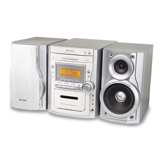
Panasonic SA-PM11 Service Manual
Hide thumbs
Also See for SA-PM11:
- Operating instructions manual (32 pages) ,
- Operating instructions manual (29 pages) ,
- Operating instructions manual (28 pages)

Related Manuals for Panasonic SA-PM11


Summary of Contents for Panasonic SA-PM11
- Page 1 ORDER NO. MD0104084C1 CD Stereo System SA-PM11 Colour (W)... White Type Area (P)... U.S.A. TAPE SECTION : AR2 MECHANISM SERIES CD SECTION : RAE0152Z-3 TRAVERSE DECK SERIES SPECIFICATIONS Specifications...
- Page 2 AMPLIFIER SECTION Power output 10% Total harmonic distortion 1 kHz, both channels driven 45 W per channel (6 70 Hz - 16 kHz, both channels driven 40 W per channel (6 Input sensitivity 250 mV Input Impedance 13 k FM TUNER SECTION Frequency range 87.9 - 107.9 MHz (200 kHz steps) 87.5 - 108.0 MHz (100 kHz steps)
- Page 3 (5 29/32” x 10 1/4” x 10 1/2”) Weight 5.6 kg (12.3 lb) SYSTEM SC-PM11(P) Music Center: SA-PM11(P) Speaker: SB-PM11(P) Notes: 1. Specifications are subject to change without notice. Weight and dimensions are aproximate. 2. Total harmonic distortion is measured by the digital spectrum analyzer.
- Page 4 jumper wire. 2. Turn on the power switch. 3. Measure the resistance value with ohmmeter between the jumper AC plug and each exposed metal cabinet part, such as screwheads, antenna, control shafts, handle brackets, etc. Equipment with antenna terminals should read between 3 M 5.2 M to all exposed parts*.(Fig.1) Equipment without antenna terminals should read approximately...
- Page 5 2. Before Repair and Adjustment Disconnect AC power, discharge Power Supply Capacitors C506, C507 and C508 through a 10 5W resistor to ground. DO NOT SHORT-CIRCUIT DIRECTLY (with a screwdriver blade, for instance), as this may destroy solid state devices. After repairs are completed, restore power gradually using a variac, to avoid overcurrent.
- Page 6 off and then on again. 4. Accessories Remote Control Transmitter FM indoor antenna AC mains lead...
- Page 7 AM Loop antenna 5. Handling Precautions For Traverse Deck The laser diode in the traverse deck (optical pickup) may break down due to potential difference caused by static electricity of clothes or human body. So, be careful of electrostatic breakdown during repair of the traverse deck (optical pickup). - Handling of traverse deck (optical pickup) 1.
- Page 8 - Grounding for electrostatic breakdown prevention 1. Human body grounding Use the anti-static wrist strap to discharge the static electricity from your body. 2. Work table grounding Put a conductive material (sheet) or steel sheet on the area where the traverse deck (optical pickup) is placed, and ground the sheet. Caution : The static electricity of your clothes will not be grounded through the wrist strap.
- Page 9 6. Precaution of Laser Diode CAUTION: This unit utilizes a class 1 laser. Invisible laser radiation is emitted from the optical pickup lens. When the unit is turned on: 1. Do not look directly into the pick up lens. 2. Do not use optical instruments to look at the pick up lens. 3.
- Page 10 8. Disassembly and Main Component Replacement Procedures...
-
Page 11: Table Of Contents
“ATTENTION SERVICER” Some chassis components may have sharp edges. Be careful when disassembling and servicing. 1. This section describes procedures for checking the operation of the major printed circuit boards and replacing the main components. 2. For reassembly after operation checks or replacement, reverse the respective procedures. - Page 12 8.1. Disassembly Procedure for each major P.C.B. checking Step 1 Remove 3 screws each side and 5 screws at rear panel. Step 2 Remove the Top Cabinet Step 3 Push catches each side. Remove 2 screws on top to release CD lid.
- Page 13 Step 4 Remove the CD changer base together with the CD changer. Step 5 Release 10 screws at rear panel. - Checking for Main P.C.B, Panel P.C.B. and Transformer P.C.B Step 1 Remove 2 screws each side.
-
Page 14: Main Component Replacement Procedures
- Checking for Power P.C.B. 8.2. Main Component Replacement Procedures 1. Replacement of the Traverse Deck Step 1 Follow the procedures in ‘Disassembly of the Traverse Unit’ ( Step 1 - Step 4 ) - Page 15 Step 3 Desolder the 4 legs of the 2 motors and pull out the Servo P.C.B. Step 4 Widen the 3 bosses with a flat screwdriver and pull out the 3 pins. Then remove the Traverse Deck.
- Page 16 Step 5 Remove the flexible cable CN 701. - Removal of the flexible cable. Push the top of the connector in the direction of the arrow 1, and then pull out the flexible cable in the direction of the arrow 2. Note: Insert a short pin into the flexible cable for traverse unit.
-
Page 17: Replacement Of The Power Amplifier Ic
Before installing the CD servo P.C.B., move the optical pickup towards the outer edge from the marking (black triangle). [Otherwise, the reset detect switch (S701) mounted on the CD servo P.C.B. may be damaged.] 2. Replacement of the Power Amplifier IC Step 1 Follow the procedures in ‘Checking Procedure for each major P.C.B.’... -
Page 18: Disassembly And Assembly Of The Traverse Unit
Step 3 Remove 4 screws fixed to the Power Amplifier IC. Step 4 Unsolder the terminals of Power Amp IC and replace the respective component. 8.3. Disassembly and assembly of the Traverse Unit Step 1 Push the lever from position A to B. Step 2 Pull the stopper (black) in the direction of arrow 1 and push the lever in the direction of arrow 2. - Page 19 Step 4 Lift up the traverse unit and slide out the unit as shown. - Replacement of Traverse Unit Step 1 Place the traverse unit as shown. Step 2 Press in the lever shaft in the direction of arrow 1 as shown and push the traverse unit into the position in the direction of arrow 2.
-
Page 20: Disassembly And Assembly Of The Disc Tray
as shown. Step 4 Pull out the tray half way and push it back fully. Step 5 Push the lever to the initial position indicated ‘I---I’. 8.4. Disassembly and assembly of the Disc Tray Step 2 With lifting the claw in the direction of arrow 1, draw the clamp SW P.C.B. in the direction of arrow 2. - Page 21 Step 4 Insert the gear with hexagonal wrench into the hole. Step 5 Rotate the hexagonal wrench in the direction of arrow (clockwise), and then open the disc tray fully. Step 6 Upset the CD changer unit again. Step 7 Release both the claws, and then draw the disc tray.
- Page 22 Step 8 With forcing the left guide bar manually because the left guide bar interfers with claw, draw the disc tray. - Installation of the disc tray after replacement Step 1 Slide the drive rack fully in the direction of arrow.
- Page 23 Step 2 Holding the drive rack not to move, install the disc tray. Step 3 Align the drive rack with the driver gear.
- Page 24 Step 4 Holding the disc tray manually, rotate the pulley gear in the direction of arrow. Step 5 Rotate the gear 5 or 6 times manually, and then push the disc tray. 9. Self-Diagnostic Function 9.1. Self-diagnostic display This unit is equipped with a self-diagnostic display function which, if a problems occur, they shall be memorised as errors and there shall be no error display at the time of such occurrence.
- Page 25 Press “STOP ” to indicate error code. - If several problem exist, error code will change each time when “STOP ” is pressed. 9.3. Cassette Mechanism Test (For error code H01, H02, H03, F01, F02)
- Page 26 1. Load a cassette tape with the erasure prevention tab, remove from left side only and close the cassette holder. 2. Press “FAST FORWARD” (Tape will be stop after 2 seconds) 3. Load a cassette tape with the erasure prevention tab, remove from right side only and close the cassette holder.
- Page 27 Error Error Problem condition Display MODE SW Faulty operation of cassette mechanism. detection error Faulty contact or short-circuit of mechanism mode switch (S951, S971). REC INH SW Recording not possible. detection error Faulty contact or short-circuit of REC INH switch S975).
- Page 28 Error Error Problem condition Display POWER AMP When POWER is switched on, power become off automatically. output abnormal During normal operation, if DC DET become L, PCNT shall become L and the error display on the left shall be displayed. (IC501) 11.
- Page 29 right channels does not exceed 5dB. 4. Perform the same adjustment in reverse playback mode. Check of the level difference forward and reverse directions 5. Playback the playback gain adjustment portion(315Hz, 0dB) of test tape(QZZCFM). Check if level difference between forward and reverse direction is within 1.5dB.
- Page 30 the middle portion of it. 3. Adjust Motor VR for the output value shown below. Adjustment target: 2940 ~ 3060 Hz (NORMAL speed) 4. After alignment, assure that the output frequency of the DECK REV is within ±60 Hz respectively of the value of the output frequency of DECK FWD.
- Page 31 2. Insert the Normal blank tape (QZZCRA) into DECK 2 and set the unit to “REC” mode ( use “REC/PAUSE” key). 3. Adjust L1301 so that the output frequency is within the standard value. Standard Value: 97 ±8 kHz 11.2. Tuner Section 11.2.1.
- Page 32 SIGNAL GENERATOR OR RADIO DIAL REMARKS INDICATOR ADJUSTMENT(Shown SWEEP GENERATOR SETTING (ELECTRONIC in Fig.1) CONNECTIONS FREQUENCY VOLTMETER OSCILLOSCOPE) Fashion a 520 kHz Tuning capacitor Headphone Jack (32 Z101 (AM OSC Coil) Adjust loop of fully closed. ) Fabricate the maximum several turns plug as shown in output.
- Page 33 Tuner Section 12. Illustration of IC’s, Transistors and Diodes 13. Terminal Function of IC’s 13.1. IC701 (AN8885SBE1) Servo Amplifier...
- Page 34 Mark Function Tracking signal input 1 Tracking signal input 2 Power supply Focus signal input terminal 1 Focus signal input terminal 2 APC amp input O APC amp output O RFsumming output RFIN Detector’s input CSBRT Capacitor for OFTR connection Capacitor for HPF amp connection O BDO output (“H”...
- Page 35 Mark Function BCLK N.C. LRCK N.C. SRDATA O N.C. DVDD1 Power supply input (for digital circuit) DVSS1 GND (for digital circuit) Digital audio interface signal output (Latches data at first transition) MCLK Microprocessor command clock signal input MDATA Microprocessor command data signal input Microprocessor command load signal input...
- Page 36 Mark Function 24 ECM Spindle motor drive signal output(forced mode output) 25 ECS Spindle motor drive signal output (servo error signal output) 26 KICK N.C. 27 TRD Tracking drive output 28 FOD Focus drive output 29 VREF D/A (drive) output (TVD, ECS, TRD, FOD, FBAL, TBAL) Reference voltage input 30 FBAL...
- Page 37 52 EFM EFM signal output Mark Function 53 PCK PLL extraction clock output (fPCK = 4.321 MHz during normal playback) 54 VCOF2 I/O VCO Loop filter for 33.8688 MHz conversation terminal for 16.9344 MHz crystal mode, must use other circuit 55 SUBC Sub-code serial data output 56 SBCK...
- Page 38 Mark Function 76 RSEL RF signal polarity assignment input (at "H" level, RSEL="H", at "L" level, RESL="L") 77 IOVOD 5V supply input 78 PSEL Test terminal (connected to Gnd) 79 MSEL SMCK oscillating frequency designation input (“L”:4.2336 MHz, “H”:8.4672 MHz) 80 SSEL SUBQ output mode select (“H”: Q-code buffer mode)
- Page 39 Mark Function PGND2 - Ground connection (2) for driver PVCC2 I Power supply (2) for driver N.C. Power supply terminal VREF Reference voltage input Motor driver (4) input Motor driver (3) input RSTIN Reset terminal N.C. 13.4. IC600 (M38258MCM084) System Microprocessor Mark Function N.C.
- Page 40 Mark Function MCLK/PLLCLK O CD command data output/Tuner PLL chip output BLKCK CD Block clock input (Inverted) STATUS CD Signal Processor status input (INV) SQCK/ST/DO Subcode clock output / Tuner IF data / Stereo Input Tuner Signal detect input SUBQ CD Subcode data input (INV) Remote control input...
- Page 41 Mark Function CHG_CCW Changer motor CCW output CHG_CW Changer motor CW output VJOG_B Main volume jog input VJOG_A Main volume jog input N.C. No connection SEG34-SEG0 Segment drive output Power supply (+5V) VREF Reference for A-D AVSS Analog ground (0V) COM3 LCD common 3 output COM2...
- Page 42 : Disc 3 switch S607 : Disc 4 switch S608 : Disc 5 switch S610 : Tuner / Band switch S611 : Tape Play select switch S612 : CD Pause switch S613 : Selector switch S614 : Stop switch S615 : Tuner/ FF switch S616 : Tune mode switch...
- Page 43 : Rev Mode switch S624 : Rec/Stop switch S701 : Reset switch S971 : Mode detect switch S972 : Leaf switch S973 : Leaf switch S974 : Leaf switch S975 : Leaf switch SW1, SW2 : Slide switch : Switch : Switch : Lower switch VR600...
- Page 44 - Importance safety notice : Components identified by mark have special characteristics important for safety. Furthermore, special parts which have purposes of fire-retardant (resistors), high-quality sound (capacitors), low-noise (resistors), etc. are used. When replacing any of components, be sure to use only manufacturer's specified parts shown in the parts list.
- Page 45 18. Troubleshooting Guide...
- Page 46 19. Parts Location and Replacement Parts List Notes:...
- Page 47 - Important safety notice: Components identified by mark have special characteristics important for safety. Furthermore, special parts which have purposes of fire-retardent (resistors), high-quality sound (capacitors), low noise (resistors), etc are used. When replacing any of these components, be sure to use only manufacturer’s specified parts shown in the parts list.
- Page 48 19.1. Deck Mechanism (RAA4109) 19.1.1. Deck Mechanism Parts Location 19.1.2. Deck Mechanism Parts List...
- Page 49 Ref. No. Part No. Part Name & Description Remarks CASSETTE DECK RED0059 R/P HEAD BLOCK UNIT RDG0300 REEL BASE GEAR RDG0301 WINDING RELAY GEAR RDK0026 MAIN GEAR RDV0033-4 WINDING BELT RDV0034-1 CAPSTAN BELT ‘A’ RMB0312 TRIGGER LEVER SPRING RMB0400 REEL SPRING RMB0403 HEAD PANEL SPRING RMB0404...
- Page 51 19.2.2. CD Loading Mechanism Parts List...
- Page 52 Ref. No. Part No. Part Name & Description Remarks TRAVERSE DECK RML0517 TIMING LEVER RML0516 PLUNGER LEVER RMB0551 UPPER SPINDLE SPRING RMQ0744 LOWER HOOK RDV0056 BELT RML0525 FRONT LOCK LEVER RML0526 DISC LEVER RDG0424 DRIVE GEAR RDG0425 CHANGE GEAR RDG0427 TRAVERSE CAM GEAR RDG0428 TRAVERSE RELAY GEAR...
- Page 53 Ref. No. Part No. Part Name & Description Remarks RDG0431 RELAY GEAR ‘B’ RME0262 DISK LEVER SP. RMA1105 SUPPORT PLATE RAE0152Z-3 TRAVERSE 358-1 SHGD113-1 FLOATING CUSHION 358-2 SNSD38 TRV MOTOR ASSY SCREW 358-3 RAF0150A-4S 50A OPTICAL PICKUP 358-4 RDG0247 DRIVE GEAR 358-5 RDG0248 RELAY GEAR...
- Page 55 19.3.2. Cabinet Parts List...
- Page 56 Ref. No. Part No. Part Name & Description Remarks CABINET AND CHASSIS RDG0357 DUMPER GEAR REEX0105 14P FFC (CD-TO-MAIN) REEX0106 19P FFC(CD-TO-PANEL) REEX0107 20P FFC REEX0108 24P FFC RGKX0073-W FRONT ORNAMENT (BTM) RGKX0074-W FRONT ORNAMENT (TOP) RGKX0072-W CD LID RGKX0080-S VOL RING ORNAMENT RGLX0031-Q PWR LIGHTING CHIP...
- Page 57 19.4. Electrical Parts List Ref. No. Part No. Part Name & Description Remarks PRINTED CIRCUITS BOARD REPX0192D CD SERVO P.C.B. [M](RTL) REPX0236A MAIN/TUNER P.C.B. [M](RTL) REPX0236A PANEL P.C.B. [M](RTL) REPX0236A TACT SWITCH (1) P.C.B. [M](RTL) REPX0236A TACT SWITCH (2) P.C.B. [M](RTL) REPX0236A HEADPHONE P.C.B.
- Page 58 Ref. No. Part No. Part Name & Description Remarks Q350 2SB621ARSTA TRANSISTOR Q351 KRC102STA TRANSISTOR Q400 KTD1304TA TRANSISTOR Q450 KTD1304TA TRANSISTOR Q501 KTC2026 TRANSISTOR Q502 KTA1046 TRANSISTOR Q503 KTA12710YTA TRANSISTOR Q504 KTA1046 TRANSISTOR Q505 KTC3199GRTA TRANSISTOR Q506 2SA933SSTA TRANSISTOR Q507 KTC3199GRTA TRANSISTOR Q508...
- Page 59 Ref. No. Part No. Part Name & Description Remarks GP1S94 DIODE SVC211SPA-AL DIODE MTZJ4R7BTA DIODE SVC211SPA-AL DIODE SVC211SPA-AL DIODE D101 UDZSTE175R1B DIODE D306 DAP202KT146 DIODE D307 DAP202KT146 DIODE D308 1SS355TE17 DIODE D309 1SS355TE17 DIODE D312 RL1N4003S-P DIODE D316 RL1N4003S-P DIODE D317 RL1N4003S-P DIODE...
- Page 60 D627 1SS380TE-17 DIODE...
- Page 61 Ref. No. Part No. Part Name & Description Remarks D628 1SS380TE-17 DIODE D630 RB751V-40 DIODE D638 1SS355TE17 DIODE D640 RB501V-40 DIODE D641 RB501V-40 DIODE D642 RB501V-40 DIODE D643 1SS355TE17 DIODE D644 1SS355TE17 DIODE D645 1SS355TE17 DIODE D646 RB501V-40 DIODE D647 RB501V-40 DIODE D648...
- Page 62 Ref. No. Part No. Part Name & Description Remarks RSH1A032-U SW, SLIDE RSH1A032-U SW, SLIDE RSH1A005-1U RSH1A91ZA-A RSP1A017-A SW, LOWER CONNECTORS RJS1A9414 14P CONNECTOR CN300 RJU100W09 9P CONNECTOR CN301 RJU100W09 9P CONNECTOR CN302 RJS2A5624 FFC CONNECTOR CN303 RJS1A9420 20P FFC TO MAIN CN304 RJS1A5209 TO MAIN MOLEX...
- Page 63 Ref. No. Part No. Part Name & Description Remarks Z501 ERZV10V511CS ZENER Z600 RSL5268-L Z602 RCDGP1U28MD REMOTE SENSOR Z971 EXBF7L355SYV RADA RESISTOR CERAMIC FILTERS CF201 RLFFETWND01M CERAMIC FILTER CF202 RLFFETWND01M CERAMIC FILTER RELAY RL502 RSY0056M-C RELAY OSCILLATORS X102 RLFDFT22DD CRYSTAL OSCILLATOR X103 RSXC7M20S05T CRYSTAL OSCILLATOR X600...
- Page 64 Ref. No. Part No. Part Name & Description Remarks WIRES REZ1023-1 4P WIRE REZ1024 3P WIRE W500 REXX0241 5P POWER TO TRANS W600 RWJ0103100SS 3P PANEL TO PANEL W601 REXX0240 4P PANEL TO TRANS W602 RWJ1110140XX 10P PANEL TO DECK W605 RWJ0206130XX 6P PANEL TO HEADP...
- Page 65 Ref. No. Part No. Part Name & Description Remarks R133 ERJ3GEYJ102V 1K 1/16W R134 ERJ3GEYJ471V 470 1/16W R135 ERJ3GEYJ102V 1K 1/16W R136 ERJ3GEYJ102V 1K 1/16W R137 ERJ3GEYJ102V 1K 1/16W R138 ERJ3GEYJ332V 3.3K 1/16W R141 ERJ3GEYJ682V 6.8K 1/16W R142 ERJ3GEYJ682V 6.8K 1/16W R143 ERJ3GEYJ223V 22K 1/16W...
- Page 66 Ref. No. Part No. Part Name & Description Remarks R346 ERJ3GEYJ223V 22K 1/16W R347 ERJ3GEYJ123V 12K 1/16W R349 ERJ3GEYJ103V 10K 1/16W R350 ERJ3GEYJ102V 1K 1/16W R351 ERJ3GEYJ103V 10K 1/16W R353 ERJ3GEYJ103V 10K 1/16W R354 ERJ3GEYJ123V 12K 1/16W R355 ERJ3GEYJ223V 22K 1/16W R358 ERJ3GEYJ473V 47K 1/16W...
- Page 67 Ref. No. Part No. Part Name & Description Remarks R509 ERDS2TJ472T 4.7K 1/4W R510 ERDS2TJ122T 1.2K 1/4W R511 ERDS2TJ182T 1.8K 1/4W R512 ERDS2TJ151T 150 1/4W R513 ERDS2TJ331T 330 1/4W R516 ERDS2TJ222T 2.2K 1/4W R517 ERDS2TJ331T 330 1/4W R518 ERDS2TJ122T 1.2K 1/4W R519 ERDS2TJ2R2T 2.2 1/4W...
- Page 68 Ref. No. Part No. Part Name & Description Remarks R584 ERDS2TJ151T 150 1/4W R586 ERDS2TJ150T 15 1/4W R587 ERC12UGK335D 3.3M 1/2W R600 ERJ3GEYJ102V 1K 1/16W R601 ERJ3GEYJ102V 1K 1/16W R602 ERJ3GEYJ122V 1.2K 1/16W R603 ERJ3GEYJ182V 1.8K 1/16W R604 ERJ3GEYJ222V 2.2K 1/16W R605 ERJ3GEYJ272V 2.7K 1/16W...
- Page 69 R705 ERJ3GEYJ154V 150K 1/16W...
- Page 70 Ref. No. Part No. Part Name & Description Remarks R706 ERJ3GEYJ102V 1K 1/16W R707 ERJ3GEYJ393V 39K 1/16W R708 ERJ3GEYJ223V 22K 1/16W R709 ERJ3GEYJ473V 47K 1/16W R711 ERJ3GEYJ823V 82K 1/16W R712 ERJ3GEYJ221V 220 1/16W R714 ERJ3GEY0R00V 0 1/16W R715 ERJ3GEYJ102V 1K 1/16W R717 ERJ3GEYJ102V 1K 1/16W...
- Page 71 Ref. No. Part No. Part Name & Description Remarks R945 ERJ3GEYJ101V 100 1/16W R946 ERJ3GEYJ101V 100 1/16W R947 ERJ3GEYJ101V 100 1/16W R948 ERJ3GEYJ472V 4.7K 1/16W R950 ERJ3GEYJ223V 22K 1/16W R951 ERJ3GEYJ102V 1K 1/16W R952 ERJ3GEYJ101V 100 1/16W R954 ERJ3GEYJ103V 10K 1/16W R955 ERJ3GEYJ562V 5.6K 1/16W...
- Page 72 Ref. No. Part No. Part Name & Description Remarks R1310 ERDS2TJ472T 4.7K 1/4W R1313 ERDS2TJ103T 10K 1/4W R1314 ERDS2TJ102T 1K 1/4W R1317 ERDS2TJ223T 22K 1/4W R1318 ERDS2TJ103T 10K 1/4W R1319 ERDS2TJ123T 12K 1/4W R1320 ERDS2TJ104T 100K 1/4W R1321 ERDS2TJ470T 47 1/4W R1322 ERDS2TJ823T 82K 1/4W...
- Page 73 Ref. No. Part No. Part Name & Description Remarks C112 ECUV1E103KBV 0.01 25V C113 ECUV1H102KBV 1000P 50V C114 ECA1HAK3R3XB 3.3 50V C115 ECA1HAK4R7XB 4.7 50V C116 ECUV1E333KBV 0.033 25V C117 ECUV1E103KBV 0.01 25V C118 ECUV1E103KBV 0.01 25V C119 ECQP2A681JZT 680P 100V C120 ECA1CAK100XB 10 16V C121...
- Page 74 Ref. No. Part No. Part Name & Description Remarks C303 ECUV1C104KBV 0.1 16V C317 ECA1HAK2R2XB 2.2 50V C318 ECUV1E103KBV 0.01 25V C319 ECA1HAK100XB 10 50V C320 ECUV1E103KBV 0.01 25V C322 ECQV1H474JZ3 0.47 50V C331 ECA1HAK4R7XB 4.7 50V C363 ECUV1H101KCV 100P 50V C364 ECUV1H101KCV 100P 50V C365...
- Page 75 Ref. No. Part No. Part Name & Description Remarks C416 ECUV1H472KBV 4700P 50V C417 ECA1HAKR33XB 0.33 50V C418 ECA1CAK100XB 10 16V C419 ECA1HAK2R2XB 2.2 50V C420 ECA1HAK2R2XB 2.2 50V C421 ECA1HAK2R2XB 2.2 50V C422 ECA1HAK4R7XB 4.7 50V C425 ECA1HAKR15XB 0.15 50V C426 ECUV1C563KBV 0.056 16V C427...
- Page 76 Ref. No. Part No. Part Name & Description Remarks C575 ECA1HAK4R7XB 4.7 50V C576 RCEA1C102B-S 1000P 16V C577 RCEA1C102B-S 1000P 16V C578 ECKR1H103ZF5 0.01 50V C580 ECKR1H103ZF5 0.01 50V C581 ECA1HM470B 47 50V C582 ECKR2H103ZF5 0.01 500V C583 ECKR1H103ZF5 0.01 50V C585 ECA1EM101B 100 25V...
- Page 77 Ref. No. Part No. Part Name & Description Remarks C707 ECUV1E273KBV 0.027 25V C710 ECUV1H121KCV 120P 50V C711 ECUV1C104ZFV 0.1 16V C712 ECUV1C104ZFV 0.1 16V C713 ECUV1C104KBV 0.1 16V C714 ECEA0JKA101I 100 6.3V C715 ECUV1H272KBV 2700P 50V C716 ECUV1H821KBN 820P 50V C717 ECUV1C104ZFV 0.1 16V C718...
- Page 78 Ref. No. Part No. Part Name & Description Remarks C1201 ECA1HAK010XB 1 50V C1202 ECBT1H102KB5 1000P 50V C1203 ECA1CAK101XB 100 16V C1204 ECFR1C273KR 0.027 16V C1205 ECBT1H471KB5 470P 50V C1206 ECA1HAK2R2XB 2.2 50V C1207 ECBT1H152KB5 1500P 50V C1208 ECA1CAK100XB 10 16V C1209 ECA1HAK3R3XB 3.3 50V C1221...
- Page 79 Ref. No. Part No. Part Name & Description Remarks RJ728 ERJ3GEY0R00V 0 1/16W RJ729 ERJ3GEY0R00V 0 1/16W RJ730 ERJ3GEY0R00V 0 1/16W RJ731 ERJ3GEY0R00V 0 1/16W RJ732 ERJ3GEY0R00V 0 1/16W RJ733 ERJ3GEY0R00V 0 1/16W RJ734 ERJ3GEY0R00V 0 1/16W RJ735 ERJ3GEY0R00V 0 1/16W RJ736 ERJ3GEY0R00V 0 1/16W RJ737...
- Page 80 Printed in Singapore / P010400001 E/H/K/J/L/PRT...
- Page 81 SCHEMATIC DIAGRAM-8 : Record signal line CASSETTE DECK CIRCUIT : +B signal line : Playback signal line C1105 470P R1103 C1122 0.01 C1102 1000P R1101 R1104 C1104 0.027 C1303 CP1301 0.033 C1302 0.033 C1307 C1106 C1108 REC/PLAY 10V220 C1101 R1302 50V2.2 16V10 50V1...
- Page 82 SCHEMATIC DIAGRAM-9 : Record signal line : +B signal line : Playback signal line Q1103, 1203 2SD1450STA R1105 MUTING SWITCH 2.2K ((0.01V)) R1107 R1109 ((0.70V)) R1106 3.9K 100K H1304 Q1101 ((0.01V)) REC_R Q1103 REC_L AFGND R1205 2.2K PB_ROUT MAIN CIRCUIT (CN304) ON ((0.01V)) PB_LOUT...
- Page 83 SCHEMATIC DIAGRAM -4 : +B Line : +B Line : Main Signal line Q250, 450 KTD1304TA HP_R SWITCH (MUTING FOR HP) HP_L Q200, 250 R249 Q250 R252 C232 C432 R449 R452 KTD1304TA R228 3300P 3300P SWITCH (MUTING) CN301 ((-2.64V)) R451 PGND R251 R248...
- Page 84 SCHEMATIC DIAGRAM -3 : Rec Signal line : AM/FM Signal line : Main Signal line MAIN CIRCUIT : +B Line : Playback Signal line : CD Signal line JK305 R401 C401 C402 R402 100P 100P 2.2K C201 C202 R202 100P 100P 2.2K R201...
- Page 85 SCHEMATIC DIAGRAM-12 MOTOR CIRCUIT : +B Signal Line TA7291P MOTOR DRIVE 50V5.6P 0.01 R1 1K MTZJ4R7BTA RVTDTC143EST POWER SUPPLY CD DETACT CONTROL PLUNGER CIRCUIT BOTTOMSW POSITION PSLED D_GND MAIN CIRCUIT P_GND (CN309) ON SCHEMATIC DIAGRAM-4 OPEN CLAMP GP1S94 DRIVEPOWER HALF SPINDLE POSITION CIRCUIT...
- Page 86 SCHEMATIC DIAGRAM-5 : +B Line : Main Signal Line PANEL CIRCUIT Z600 RSL5268-L 9 10 11 12 13 14 15 16 17 18 19 20 21 22 23 24 25 26 27 28 29 30 31 32 33 34 35 36 37 38 39 TACT SWITCH (1) IC601 BU2090AF-E2...
- Page 87 SCHEMATIC DIAGRAM-6 : +B Line : CD Signal Line 64 63 SEG10 ((2.31V)) ((5.17V)) SEG9 V_JOGA ((2.30V)) ((5.15V)) C624 SEG8 V_JOGB 6.3V100 ((2.30V)) ((5.13V)) SEG7 CHG_CW C623 ((5.11V)) ((2.30V)) CHG_CCW SEG6 ((2.28V)) ((0V)) SEG5 CHG_HALF C625 R922 R678 ((2.30V)) ((0V)) L603 CHG_PLGR 6.3V1000P...
- Page 88 SCHEMATIC DIAGRAM-7 : +B Line : Main Signal Line : CD Signal Line H600 LED15V MOTOR MOTOR SYS6V2 R966 R964 R965 PLGR PLGR SYS6V D649 R968 DVREF+ DVREF+ R642 D648 5.6K 3.9K DECK_AD1 CASSETTE DECK_AD1 DECK CIRCUIT DECK_AD2 DECK_AD2 (CN1303) on DVREF+ D601 D605...
- Page 89 SCHEMATIC DIAGRAM-13 : -B Signal line POWER CIRCUIT : Main Signal line : +B Signal line IC501 IC501 RSN35H1A-P POWER IC +INL -INL -INR +INR GND LATCHC LCH SPK MAIN CIRCUIT R554 330K (CN500A) on RCH SPK SCHEMATIC R532 R534 DIAGRAM-4 R540 C543...
- Page 90 SCHEMATIC DIAGRAM-14 : +B signal line TRANSFORMER CIRCUIT R581 R580 D581 D578 Q577 2SC3940AQSTA SYS 6V SWITCH (REG) C585 C576 25V100 D579 16V1000 Q577 ((5.97V)) ((9.21V)) C578 0.01 ((6.63V)) C580 R583 0.01 R584 C577 D580 16V1000 C581 D582 50V47 C582 0.01 R586 D577...
- Page 91 SCHEMATIC DIAGRAM-10 : +B signal line : AM signal line TUNER CIRCUIT(MAIN) : FM OSC Signal line : AM OSC Signal line : FM signal line TUNER PACK CIRCUIT 2SK544 2SC2786M C103 5.6P 0.01 R107 RF AMP FM MIXER CF201 2.2P RLFFETWND01M 0.47u...
- Page 92 SCHEMATIC DIAGRAM-11 : AM signal line : +B signal line : FM signal line : FM/AM signal line R104 CF202 R101 RLFFETWNDO1M R121 Q106 C120 16V10 Q106 ((0.6V)) ((14.56V)) KRA102MTA TUNER SUPPLY R143 C138 SWITCH 0.01 ((14.52V)) C117 C139 C118 C142 R142 0.01...
- Page 93 OPTICAL PICKUP IC701 AN8885SBE1 SERVO AMP SEMICONDUCTOR LASER OFTR TENV DET. Q701 LASER POWER DRIVE OFTR OFTR DET. LDON /RFDET /RFDET DET. PHOTO DETECTOR FEOUT Subtracter VCBA VREF Subtracter VCBA N.C. TRACKING FOCUS COIL COIL TX 6 SYNDROME DIGITAL AUDIO CALCULATION INTERFACE PHASE...
- Page 94 FM ANT AM ANT Z101 (FM) CF201 CF202 Z120 Q101 COIL COIL MIXER IF AMP RF AMP IC101 LA1833NMNTLM BUFFER FM/AM IF AMP, DET/AM OSC, MIX/FM MPX (FM) DECODER RF AMP PILOT BUFFER PHASE CANCEL LEVEL STEREO S-CURVE SWITCH AM/FM COMP BUFFER TUNING...
- Page 95 TA7291P MOTOR DRIVE OUT1 OUT2 POWER SUPPLY CONTROL Q350 MOTOR Q902 SUPPLY SWITCH STATUS SWITCH Q901 SUBQ SWITCH Q351 SWITCH SQCLKST/DO Q903 BLKCK SWITCH /CDRST RESTSW D644 CE/MLD MLD/PLLCE DI/MDATA MDATA/PLLDA MICROPROCESSOR IC600 M38258MCM084 CL/MCLK MCLK/PLLCK...
- Page 96 FILTER Q1103(Q1203) R/P HEAD Q1101 (L ch) MUTING (Q1201) SWITCH MUTING SWITCH IC1001 AN7326K FILTER P/B REC AMP 22(1) 21(2) 20(3) 19(4) RIPPLE REJECTION LOGIC REC AMP (L) MUTE SWITCHING IC1000 BA7755A ANALOG SWITCH Q1302 DECK MUTING CONTROL Q1304 REC_H SWITCH Q1308 SWITCH...
- Page 97 HP_L(R) FILTER Q250(Q450) (10) (13) (14) (16) (20) (21) (22) (59) SWITCH 45(46) INLC(R) IC302 43(44) M5218AP Q400(Q200) INLB(R) 32(31) 51(52) OP AMP OUTL(R) SWITCH RECL(R) IC301 BH3874AKS2 41(42) FROM CD SIGNAL INLA(R) CD UNIT 47(48) INLD(R) Q202 JK305 (Q201) Q306 AGC CONTROL SWITCH...
- Page 98 SIGNAL LINES MAIN SIGNAL LINE CD SIGNAL LINE AM SIGNAL LINE PLAYBACK SIGNAL LINE FM OSC SIGNAL LINE AM OSC SIGNAL LINE FM & AM SIGNALS LINE RECORDING SIGNAL LINE AUX SIGNAL LINE FM SIGNAL LINE IC501 RSN35H1A-P POWER IC 11(13) 10(14) 4(1)
- Page 99 BU2090AF-E2 (16P) AN8739SBE2 MN662790RSC (80P) TA7291P RSN35H1A-P BA7755A LA1833NMNTLM (24P) AN7326K M38258MCM084 (100P) LC72131MDTRM (20P) BH3874AKS2 (64P) AN8885SBE1 (28P) 0N2180RLC KTC2026 2SB1238QRTV2 M5218AP AN7326K 2SC2058SPTA KTA1046 2SD1859QRTV2 2SB1417PQTA KRA102MTA KTA12710YTA 2SC1845FTA 2SA933SSTA KRA110MTA KTA1504GRTA 2SC2001LTA 2SC2787FL1TA KRC102MTA KTC32030YTA 2SD965RTA 2SC2786MTA KRC103MTA KRC101MTA 2SD1450STA...
- Page 100 MOTOR P.C.B (REP2578A-N) 1 2 3 4 5 6 7 8 9 10 2 3 4 CD DETACT P.C.B SPINDLE POSITION P.C.B (REP2578A-N) (REP2578A-N) 1 2 3 4 TUNER PACK P.C.B (REP1999B)
- Page 101 DECK P.C.B. (REPX0240A) C1303 C1106 J1020 R1321 C1109 R1322 J1021 C1105 C1304 R1320 R1303 R1318 C1306 C1122 R1344 R1307 IC1001 C1307 R1343 R1317 J1004 C1221 C1308 C1203 R1308 J1005 C1201 J1023 J1018 R1201 J1024 R1345 W1903 J1006 C1202 J1101 C1206 J1102 R1202 C1209...
- Page 102 MAIN / TUNER P.C.B. (REPX0236A) AM LOOP FM LOOP ANTENNA ANTENNA SPEAKERS C438 JK101 J130 J131 C107 C238 R112 Z120 (TUNER PACK) J100 Z101 J248 J247 J127 J126 J125 J124 J123 R106 R103 R104 C300 J243 J135 Q106 J241 J242 C102 J240 J121...
- Page 103 PANEL P.C.B. (REPX0236A) J299 Z600 R684 S620 J294 R658 J446 R660 J427 R659 R922 R618 J434 J368 J288 L603 S621 C632 C624 IC601 C633 IC600 J277 R984 C629 SOUND EQ J281 R904 J366 C615 R902 J364 C623 J275 J409 C616 J274 J363 C625...
- Page 104 J298 R967 D607 R968 J296 J372 J371 R687 R952 Q609 C664 C656 R642 C662 R931 R917 J292 C663 R925 C657 X601 R919 J289 Q607 J287 R960 C655 J286 R948 J285 C652 R926 R964 R965 J283 CLK/TMR R915 R966 DEMO R696 R923 R601 J365...
- Page 105 POWER P.C.B. (REPX0237A) CP500 CP501 JK501 J529 J590 J530 J507 J587 R536 C511 R549 R512 C512 Q517 C514 D515 J577 J565 R513 J570 D516 C513 R518 D520 J580 J581 C521 R507 J582 D541 D517 C533 C553 C554 R542 C523 R544 R553 C540 C507...
- Page 106 CD SERVO P.C.B (REPX0192D) (RF) TP20 X701 TJ701 TP23 C717 R714 TP19 TP21 TP29 C716 C721 R709 C744 TP24 C722 R712 TP18 C723 C724 R742 C725 TP25 IC701 TP26 TP27 C731 C753 TP22 C754 C711 J702 C718 C712 IC702 C713 J712 R705 C747...
- Page 107 TACT SWITCH (1) P.C.B. (REPX0236A) R616 S619 S618 W600B TACT SWITCH (2) P.C.B. (REPX0236A) S607 S606 S605 S608 S604 R610 R602 R609 R608 CP600 R607 S613 S611 S610 R611 R613 S614 HEAD PHONE P.C.B. (REPX0236A) L601 J301 L602 H605B/W605B C612 JK600 R621 R622...
- Page 108 AC TRANSFORMER P.C.B. (REPX0237A) R578 JK500 D577 J517 J518 CN502 C575 J519 J520 AC IN RL502 120V 60HZ R587 D588 J552 J551 D584 J576 PRIMARY SECONDARY R583 C582 R579 C585 D581 J532 R580 R581 C576 J600 C580 C578 C577 D580 C581 R584 R586...
- Page 109 SCHEMATIC DIAGRAM -1 : +B SIGNAL LINE : +B SIGNAL LINE : CD SIGNAL LINE CD SERVO CIRCUIT R701 OPTICAL PICKUP CIRCUIT Q701 C701 2SA1037AKSTX 6.3V33 3.2V C703 LASER POWER DRIVE LASER DIODE 6.3V100 Q701 CN701 2.7V ((2.3V)) 0.9V ((2V)) C704 R750 LD GND...
- Page 110 SCHEMATIC DIAGRAM - 2 : +B SIGNAL LINE : +B SIGNAL LINE : CD SIGNAL LINE R717 C727 50V1 C725 1000P R721 C726 1000P R718 C728 50V1 C731 6.3V220 CN702 Lch OUT C730 C733 C732 A.GND 6.3V220 C754 Rch OUT 470P +3.3V C753...
Need help?
Do you have a question about the SA-PM11 and is the answer not in the manual?
Questions and answers
Por que no abre la tapa donde va los tapa? why doesn`t the cover where the panasonic SA-PM11 equipment tapes go open?