Table of Contents
Advertisement
Quick Links
Jan. 2014
Table of Contents
Cautionary Notes ..............................................................2
Specifications .....................................................................3
Location of Controls .........................................................4
Location of Controls Parts List........................................5
Exploded View (All) .........................................................6
Exploded View (All) Parts List........................................7
Disassembly Procedure ....................................................7
Important Notes on Assembly ........................................7
Plane View (1)....................................................................8
Plane View (1) Parts List ..................................................8
Plane View (2)....................................................................9
Plane View (2) Parts List ..................................................9
Exploded View (Fig. A)..................................................10
Exploded View (Fig. A) Parts List ................................10
Exploded View (Fig. B)...................................................11
Exploded View (Fig. B) Parts List .................................11
Copyright © 2014 Roland Corporation
All rights reserved. No part of this publication may be reproduced in any form without the written permission
of Roland Corporation.
Parts List ...........................................................................12
Verifying the Version......................................................14
Virus Check ......................................................................14
Data Backup and Restore Operations ..........................14
Performing a Factory Reset............................................14
Updating the System ......................................................14
Test Mode .........................................................................14
Block Diagram .................................................................24
Circuit Board (Main Board) ...........................................26
Circuit Diagram (Main Board: 1/4) ..............................28
Circuit Diagram (Main Board: 2/4) ..............................30
Circuit Diagram (Main Board: 3/4) ..............................32
Circuit Diagram (Main Board: 4/4) ..............................34
Circuit Board (Panel, Jack, EXP Board) ........................36
Circuit Diagram (Panel Board)......................................38
Circuit Diagram (Jack, EXP Board)...............................40
Revise Information
May 22, 2014
17058912E0
SERVICE NOTES
Issued by RJA
p. 22, p. 23
Corrected errors.
ME-80
CC-OKN
Advertisement
Table of Contents

Related Manuals for Roland ME-80


Summary of Contents for Roland ME-80
-
Page 1: Table Of Contents
Circuit Diagram (Jack, EXP Board).......40 Revise Information May 22, 2014 p. 22, p. 23 Corrected errors. Copyright © 2014 Roland Corporation All rights reserved. No part of this publication may be reproduced in any form without the written permission of Roland Corporation. 17058912E0 CC-OKN... -
Page 2: Cautionary Notes
• Because reissuance is restricted. • Because the part is made to order (at current market price). • Because it is carried in electronic data on the Roland web site. • Because it is a package or an accessory irrelevant to the function maintenance of the main body. -
Page 3: Specifications
24 bits + AF method Alkaline battery (AA, LR6) x 6 * AF method (Adaptive Focus method) This is a proprietary method from Roland Carbon-zinc battery (AA, R6) x 6 & BOSS that vastly improves the signal-to-noise (SN) ratio of the AD and DA converters. -
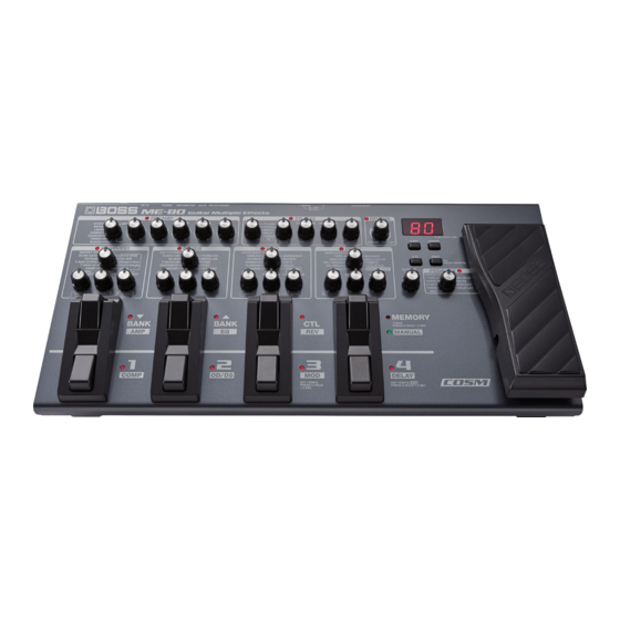
Page 4: Location Of Controls
Jan. 2014 ME-80 Location of Controls fig.panel.eps... -
Page 5: Location Of Controls Parts List
Jan. 2014 ME-80 Location of Controls Parts List Part Code Part Name Description Q’ty 5100037540 TOP COVER 03344934 R-KNOB (75D522N0R0) 5100037572 ROTARY POTENTIOMETER RD901F-40-125F-B50K-09D 03344934 R-KNOB (75D522N0R0) 5100001449 POTENTIOMETER (F3279804R0) RD901F-40-125F-B50K-06D 03344934 R-KNOB (75D522N0R0) 5100001455 ROTARY POTENTIOMETER RD901F-40-125F-B50K-0DD 03344934 R-KNOB... -
Page 6: Exploded View (All)
Jan. 2014 ME-80 Exploded View (All) fig.bunkai-all.eps Refer to Fig. B Refer to Fig. A... -
Page 7: Exploded View (All) Parts List
Remove screws d (11) in View 2 (Plane View (1) (p. 8)). Lift the Bottom Cover slightly and detach the wiring (1) connecting the On the ME-80, not all potentiometers use potentiometer nuts. Main Board and the Battery Case Set. -
Page 8: Plane View (1)
Jan. 2014 ME-80 Plane View (1) fig.heimen1.eps View 1 View 2 Plane View (1) Parts List View 1 Part Code Part Name Description Q’ty 40019123 SCREW 3X8 BINDING TAPTITE S BZC 40342712 SCREW M3X6 PAN MACHINE W/SW+SMALL PW BZC View 2... -
Page 9: Plane View (2)
Jan. 2014 ME-80 Plane View (2) fig.heimen2.eps View 3 View 4 Plane View (2) Parts List View 3 Part Code Part Name Description Q’ty 40011278 SCREW 3X8 BINDING TAPTITE P FE ZC 40017934 SCREW M3X6 PAN MACHINE W/SW+PW(L) FE ZC... -
Page 10: Exploded View (Fig. A)
Jan. 2014 ME-80 Exploded View (Fig. A) fig.bunkai-A.eps Exploded View (Fig. A) Parts List Part Code Part Name Description Q’ty 5100037546 SW PEDAL REAR 5100037545 SW PEDAL FRONT 04560712 SUPPORT SPRING (G2177103R0) 5100037544 SW PEDAL ESCUTCHEON 5100003910 PEDAL FOOT H=7.6... -
Page 11: Exploded View (Fig. B)
Jan. 2014 ME-80 Exploded View (Fig. B) fig.bunkai-B.eps Exploded View (Fig. B) Parts List Part Code Part Name Description Q’ty 5100011395 PEDAL PLATE 5100011392 VR PEDAL 04560589 WASHER M6 T1 (H5039122) 5100012929 HEX BOLT M6X50 HALF THREAD BZC 04560601 CUSHION... -
Page 12: Parts List
Jan. 2014 ME-80 Parts List fig.-part1-e.eps Due to one or more of the following reasons, Safety Precautions: parts with parts code ******** cannot be supplied as service parts. The parts marked have safety-related characteristics. Use only listed parts for replacement. - Page 13 Jan. 2014 ME-80 SCREWS 40342712 SCREW M3X6 PAN MACHINE W/SW+SMALL PW BZC 40017934 SCREW M3X6 PAN MACHINE W/SW+PW(L) FE ZC 40019123 SCREW 3X8 BINDING TAPTITE S BZC 40011278 SCREW 3X8 BINDING TAPTITE P FE ZC 40011312 SCREW 3X8 BINDING TAPTITE P FE BZC...
-
Page 14: Verifying The Version
Before connecting your computer to the ME-80, carry out a virus check Verify that the reading on the 7-segment LED display changes to U.P and on the ME-80. If it has been infected by a virus, format it after obtaining the dot is flashing. - Page 15 Jan. 2014 ME-80 Connection Diagram fig.connection-e.eps Entering the Test Mode Refer to the connection diagram, connect the respective pieces of equipment. Adjust the PEDAL FX control to FREEZE. Turn down all controls other than the PEDAL FX control all the way counterclockwise (minimum).
- Page 16 Jan. 2014 ME-80 1. Version Check and Device Check 2. Current-consumption Check, Voltage Detection Check and SW/LED Check When entering the Test Mode, the device check begins automatically. * When no USB cable is connected, an error is displayed. Verify that all LEDs are lighted.
- Page 17 Jan. 2014 ME-80 3. VR Test Verify that 11 is shown on the 7-segment LED display. fig.test3-1.eps * If 11 is not shown on, turn down all controls all the way counterclockwise (minimum) and verify that the reading changes to 11.
- Page 18 Jan. 2014 ME-80 Verify that 71 is shown on the 7-segment LED display. fig.test3-9.eps VR knob VR position and reading on the 7-segment LED display EQ/FX2 TYPE fig.test3-10-e.eps EQ/FX2 BASS fig.test3-11-e.eps EQ/FX2 MIDDLE fig.test3-12-e.eps EQ/FX2 TREBLE fig.test3-13-e.eps EQ/FX2 LEVEL fig.test3-14-e.eps REVERB fig.test3-15-e.eps...
- Page 19 Jan. 2014 ME-80 Verify that 31 is shown on the 7-segment LED display. fig.test3-16.eps VR knob VR position and reading on the 7-segment LED display DELAY TYPE fig.test3-17-e.eps MOD TYPE fig.test3-18-e.eps OD/DS TYPE fig.test3-19-e.eps COMP/FX1 TYPE fig.test3-20-e.eps COMP/FX1/SUSTAIN/ fig.test3-21-e.eps SENS/-1OCT COMP/FX1/ATTACK/ fig.test3-22-e.eps...
- Page 20 Jan. 2014 ME-80 Verify that 1 is shown on the 7-segment LED display. fig.test3-25.eps VR knob VR position and reading on the 7-segment LED display OD/DS TONE fig.test3-26-e.eps OD/DS LEVEL fig.test3-27-e.eps MOD/RATE/KEY fig.test3-28-e.eps MOD/DEPTH/HARMONY fig.test3-29-e.eps MOD/E.LEVEL/RESONANCE fig.test3-30-e.eps DELAY TIME fig.test3-31-e.eps DELAY FEEDBACK fig.test3-32-e.eps...
- Page 21 Jan. 2014 ME-80 Verify that 9 is shown on the 7-segment LED display. fig.test3-34.eps VR knob VR position and reading on the 7-segment LED display OUTPUT LEVEL fig.test3-35-e.eps PEDAL FX TYPE fig.test3-36-e.eps 4. EXP VR Check 5. AUDIO Check The 7-segment LED display shows Pd, then UP appears.
- Page 22 Jan. 2014 ME-80 Verify that the output value is between 4.9 and 5.2 Vp-p. A/D Check fig.test5-3.eps Make the settings shown below on the oscillator and connect it for input to the GUITAR INPUT jack. 200-Hz sine wave at 2.0 Vp-p Make the settings shown below on the oscilloscope and connect it to the Gt.
- Page 23 Jan. 2014 ME-80 MUTE Check OUTPUT MONO Check Make the settings shown below on the oscilloscope and connect it to the Set the signal generator as shown below, and perform input only to the R Gt. AMP OUTPUT L/MONO and R jacks.
-
Page 24: Block Diagram
Jan. 2014 ME-80 Block Diagram fig.block.eps@L... - Page 25 Jan. 2014 ME-80 fig.block.eps@R...
-
Page 26: Circuit Board (Main Board)
Jan. 2014 ME-80 Circuit Board (Main Board) fig.b-main1.eps... - Page 27 Jan. 2014 ME-80 fig.b-main2.eps...
-
Page 28: Circuit Diagram (Main Board: 1/4)
Jan. 2014 ME-80 Circuit Diagram (Main Board: 1/4) fig.d-main1.eps@L D+3.3 1SS362FV(TPL3) TP77 TP11 TP13 1SS387(TPH3.F) XSWD-PWR UnPop TP14 DTA114TUAT106 SPUP192000 From CPU 1SS361FV(TPL3.Z) TP10 H->POWER ON SPUP192000 XPWR-OFF L->POWER OFF C117 UnPop PVCC MCH6341-TL-E SR24 DC IN KM02018ABM1P 1608 220uF 0.1uF... - Page 29 Jan. 2014 ME-80 fig.d-main1.eps@R AVCC AVCC PVCC D+1.2 2SC4738-GR(TE85L.F) C257 C258 C259 C260 C261 C262 C255 C256 2.2k 0.1uF 0.1uF 0.1uF 0.1uF 0.1uF 0.1uF 0.1uF 0.1uF 1608 TP34 47uF 47uF D+1.2 TP32 TP30 ELL6SH820M 2012 82uH QS5U27TR(PB FREE) 0.1uF 47uF 0.1uF...
-
Page 30: Circuit Diagram (Main Board: 2/4)
Jan. 2014 ME-80 Circuit Diagram (Main Board: 2/4) fig.d-main2.eps@L D+3.3 JTAG for ESC 2 R117 D+3.3 XPWR-OFF M1 8 M1 9 XOUTPUT-MUT E M2 0 MA(0:15 ) M2 1 XCODEC-PDN MA(15) XICE-RS T AA15 MA(14) W1 6 MA(10) CN 3 D+1.2... - Page 31 Jan. 2014 ME-80 fig.d-main2.eps@R MD(0:15 ) MD(15) DQ1 5 MA(14) MD(14) DQ1 4 MA(15) MD(13) DQ1 3 MD(12) DQ1 2 MA(11) MD(11) DQ1 1 MA(10) MD(10) A10/AP DQ1 0 MA(9) MD(9) DQ 9 MA(8) MD(8) DQ 8 MA(7) MD(7) DQ 7...
-
Page 32: Circuit Diagram (Main Board: 3/4)
Jan. 2014 ME-80 Circuit Diagram (Main Board: 3/4) fig.d-main3.eps@L AVCC A2001WV2-6P TO JACK BOARD CN400 AVCC UnPop AUX Lch AUX Rch 10uF AUX IN 10uF 1000pF 1000pF HTJ-035-10ABZ CODEC-BCK CODEC-MCK CODEC-LRCK XCODEC-PDN f1=8.67kHz f2=1.287kHz A+3.3 Gain=-16.57dB Gain=-6.72dB R243 C204 47pF C254 6.8k... - Page 33 Jan. 2014 ME-80 fig.d-main3.eps@R UnPop Gain=+6.72dB f1=8.67kHz R130 C113 6.8k f2=1.287kHz 2700pF D (0.5%) Gain=-16.57dB C108 47pF R116 C155 R102 10uF C102 D (0.5%) R132 10uF 10uF D (0.5%) NJM4556AM(TE2) D (0.5%) 100k DTC614TU T106 AVREF1 R128 C112 6.8k 1500pF D (0.5%)
-
Page 34: Circuit Diagram (Main Board: 4/4)
Jan. 2014 ME-80 Circuit Diagram (Main Board: 4/4) fig.d-main4.eps D+3.3 28FMN-STK-A (LF)(SN) EXP-VR VR1-COM VR2-COM VR3-COM VR4-COM MUX-A MUX-B MUX-C LED-CLK LED-DATA1 LED-DATA2 TO PANEL BOARD CN2 LED-DATA3 SW-1 SW-2 SW-3 SW-4 SW-5 SW-6 SW-7 SW-8 SW-9 SW-10 SW-11 SW-12... - Page 35 Jan. 2014 ME-80...
-
Page 36: Circuit Board (Panel, Jack, Exp Board)
Jan. 2014 ME-80 Circuit Board (Panel, Jack, EXP Board) fig.b-panel1.eps... - Page 37 Jan. 2014 ME-80 fig.b-panel2.eps...
-
Page 38: Circuit Diagram (Panel Board)
Jan. 2014 ME-80 Circuit Diagram (Panel Board) fig.d-panel1.eps@L VR10 VR10 VR11 VR11 VR12 VR12 VR13 VR13 VR14 VR14 VR15 VR15 VR16 VR16 VR17 VR17 VR18 VR18 VR19 VR19 VR20 VR20 VR21 VR21 VR22 VR22 VR29 VR29 VR30 VR30 VR23 VR23... - Page 39 Jan. 2014 ME-80 fig.d-panel1.eps@R D+3.3 TO EXP BOARD CN30 0 CN 1 A2001WR2-3P 10uF 0.1u F D+3.3 100uF GN D GN D 0.1u F D+3.3 D+3.3 7Seg:typ 3.2mA, min 2.3m CN 2 28FMN-STK-A (LF)(SN GN D 100uF Q1 1 LED20...
-
Page 40: Circuit Diagram (Jack, Exp Board)
GUITAR INPUT C401 R400 HTJ-064-12IMP 6Y1H105J-T2 C400 MK400 10pF C403 10uF R404 TO MAIN BHOARD CN5 CN400 GT-3 JACK SHIELD COVER ME-80 WIRING W2(INPUT) AVCC IN-AVREF R403 C402 R406 10uF JACK BOARD VR300 VR300 RK11K1140AFG RK11K1140AFG VR300 TO PANEL BOARD CN1...
Need help?
Do you have a question about the ME-80 and is the answer not in the manual?
Questions and answers