
Related Manuals for Technics SL-DZ1200PP


Summary of Contents for Technics SL-DZ1200PP
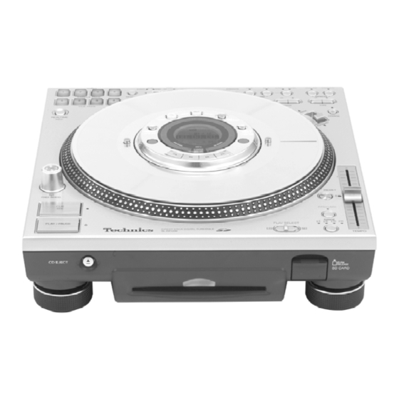
- Page 1 ORDER No.AD0404041C0 Direct Drive Digital Turntable SL-DZ1200PP / SL-DZ1200EB / SL-DZ1200EG / SL-DZ1200EP / SL-DZ1200GN Colours (S)....Silver Type SPECIFICATIONS Specification...
- Page 2 Playable media CD (12 cm) (5”): CD-Audio (CD-DA) / CD-R/CD- RW (CD-DA, MP3) SD Memory Card CD-MP3 player format Compatible compression rate: between 32 kbps and 192 kbps / (Recommended: 128 kbps) Compatible sampling rate: 48 kHz/44.1 kHz/32 kHz SD Audio play format Audio extension format: MPEG2-AAC/MP3 Compatible sampling rate:...
-
Page 3: Safety Precaution
1. Safety Precaution (This “Safety Precaution” is applied only in U.S.A.) 1. Before servicing, unplug the power cord to prevent an electric shock. 2. When replacing parts, use only manufacturer’s recommended components for safety. 3. Check the condition of the power cord. Replace if wear or damage is evident. - Page 4 (Fig. B)
-
Page 5: Caution For Ac Mains Lead
4. If the measurement is outside the specified limits, there is a possibility of a shock hazard. The equipment should be repaired and rechecked before it is returned to the customer. 2. Caution for AC Mains Lead 3. Handling Precautions for Optical pick-up The laser diode in the optical pick-up may break down due to potential difference caused by static electricity of clothes or human body. -
Page 6: Handling Of Traverse Deck Optical Pick-Up
3.1. Handling of traverse deck optical pick-up 1. Do not subject the optical pick-up to static electricity as it is extremely sensitive to electrical shock. 2. To protect the laser diode against electrostatic breakdown, short the flexible board (FFC board) with a clip or similar object. Refer Fig. -
Page 7: Precaution Of Laser Diode
Caution: The static electricity of your clothes will not be grounded through the wrist strap. So take care not to let your clothes touch the optical pick-up. 4. Precaution of Laser Diode 5. Accessories - AC power supply cord for (PP) area / (REZ1619)....1 pc. - Page 8 - AC mains lead for (EB) area / (REZ1496)....1 pc. - AC mains lead for (EG),(EP) areas / (REZ1495)....1 pc. - AC mains lead for (GN) areas / (REZ1620)....1 pc. - Stereo connection cable for all areas / (SFDHBD2N01)....1 - Slip surface for all areas / (RGK1704-S2)....1 pc.
- Page 9 6. Main features 7. Component part names 8. Operation Checks and Component Replacement Procedures - This section describes procedures for checking the operation of the major printed circuit boards and replacing the main components. - For reassembly after operation checks or replacement, reverse the respective procedures.
- Page 10 8.2. Checking for the main P.C.B. - Follow the (Step 1) - (Step 3) of item 8.1. - Check the main P.C.B. (A side) as shown below. - Check the main P.C.B. (B side) as shown below. 8.3. Checking for the jack P.C.B. - Follow the (Step 1) - (Step 3) of item 8.1.
- Page 11 - Check the jack P.C.B. as shown below. 8.4. Checking for the power supply P.C.B. - Follow the (Step 1) - (Step 3) of item 8.1. - Check the power supply P.C.B. as shown below.
- Page 12 8.5. Checking for the CD servo P.C.B. - Follow the (Step 1) - (Step 3) of item 8.1. - Follow the (Step 1) of item 8.2.
- Page 13 8.6. Replacement for the LED P.C.B., loading motor P.C.B., CD mouse ass’y and motor - Follow the (Step 1) - (Step 3) of item 8.1. - Follow the (Step 1) of item 8.2. - Follow the (Step 1) - (Step 9) of item 8.5.
-
Page 15: Replacement For The Center Panel Ass'y And Lcd
8.7. Replacement for the center panel ass’y and LCD... - Page 16 8.8. Replacement for the connection P.C.B. and sensor P.C.b. - Follow the (Step 1) - (Step 6) of item 8.7.
-
Page 17: Replacement For The Turntable Ass'y And Slip Plate Ass'y
8.9. Replacement for the turntable ass’y and slip plate ass’y - Follow the (Step 1) - (Step 6) of item 8.7. - Follow the (Step 1) - (Step 5) of item 8.8. - Page 19 8.10. Replacement for the control panel (2) P.C.B., button base B and button base C. - Follow the (Step 1) - (Step 3) of item 8.1.
- Page 20 8.11. Replacement for the control panel (1) P.C.B., reverse switch P.C.B., button base A and button base D - Follow the (Step 1) - (Step 3) of item 8.1.
- Page 21 8.12. Replacement for the CD servo P.C.B.
- Page 22 - Follow the (Step 1) - (Step 3) of item 8.1. - Follow the (Step 1) of item 8.2. - Follow the (Step 1) - (Step 9) of item 8.5. - Follow the (Step 1) - (Step 4) of item 8.6.
- Page 23 8.13. Replacement for the optical pick-up - Follow the (Step 1) - (Step 3) of item 8.1. - Follow the (Step 1) of item 8.2. - Follow the (Step 1) - (Step 9) of item 8.5. - Follow the (Step 1) - (Step 4) of item 8.6. - Follow the (Step 1) - (Step 5) of item 8.12.
- Page 25 - Grease PART NO.: RFKXPG641...
-
Page 26: Device Test
9. Technological Explanation of the Circuit and Signal 10. Self-diagnosis function - Start by switching on the power while pressing EXECUTE, SAMPLE PAD3 for the finished product. / Select the following pages with the buttons (||<< and >>||) at the lower part of the LCD. 10.1. -
Page 27: Tt Brake Test
by real-time REC button operation or escape to page 1. 10.2. TT BRAKE TEST - Set the brake to the maximum for FAST and press the start button with a CD inserted. (Please Wait is displayed for some time.) / Press the [FAST] button when steady rotation has been reached. -
Page 28: Tt Speed (Phase) Test
10.3. TT SPEED (Phase) TEST - Press the start button with a CD inserted, move the tempo slider sequentially to 0, +50%, and -50%, and press [TEST]. / (Perform this operation manually. This also serves for inspection of the slider itself).At this time, automatic counting is performed on the inside (a measuring time of TT 1.5 revolutions each is required), and when the upper and lower limit range set in advance is not exceeded, OK is displayed on the LCD, while NG is displayed... -
Page 29: Sw&Led Test
[TEST] is pressed. In case of NG, a defect of the shaft in case of a mechanical fault, a defective servo constant in case of an electrical defect, or defective parts can be assumed. 10.4. SW&LED TEST - Press [TEST] to start the inspection. - Each time a switch on the control panel is pressed, the LED near the switch lights, so that the operation can be confirmed. - Page 30 are not inspection objects. 10.5. LED TEST - Press [TEST] to start the inspection. - The LCD display is changed with the two switches at the lower part of the LCD. (<< >>) / (||<<. >>||) on both sides are switches for page switching in the sameway as for the other pages, and this should be noted.
- Page 31 abnormality. 10.7. INITIAL - When [INIT] is pressed, initialization to the factory preset values is performed, and the settings for 50 media CUEPAD, LOOP, and AUTOCUE and the LCD display angle are initialized. (The LCD contrast is changed to no change.)
-
Page 32: Cd Unit Test
10.8. CD UNIT TEST 1 - When a CD is inserted and start is performed, the first five seconds of the first title are played, the first five seconds of the last title are played, and then the CD is ejected. / If the unit is left in this condition, automatic reloadingis performed after 10 seconds, and then the operation from playing of the first five seconds of the first title on is repeated endlessly. -
Page 33: Cautions After Exchange Of The Flash Rom (Ic23)
11. Cautions after Exchange of the Flash ROM (IC23) This unit uses a flash ROM (IC23) for the program ROM. The program in the flash ROM (IC23) can be written and rewritten electrically. With this unit, an SD card with a written program is inserted in advance into the main unit, and thenthe program is written to the flash ROM (IC23). - Page 34 3. Use the USB Reader/Writer to copy DZ12SC.DAT and DZ12MD.DAT from the personal computer to the root of the SD card. 11.1.1. Method of Program Download 1. The “Program” can be downloaded from TSN SYSTEM. A. Access to TSN SYSTEM (URL---http:// tsndb.css.panasonic.co.jp).
- Page 35 3. The lamps of the CUE PADS {1} and {2} light and writing to the flash ROM (IC23) starts. 4. Afterwards, the CUE PADS {3} and {4} automatically light in sequence, and finally the lamps of all CUE PADS/SAMPLE PADS light and writing is completed.
-
Page 37: Program Confirmation
11.3. Program Confirmation The program of the flash ROM (IC23) can be confirmed according to the following procedure. 1. Press button {1} of the SAMPLE PADS and the EXECUTE button at the same time for at least 5 seconds. 2. The CD version is displayed on the LCD as Version (Example: V 1.7). - Page 38 11.4. Adjusting the Display Contrast Adjust the contrast of the LCD after replacement of IC23 if the contrast is very strong or very weak. 1. Press and hold [~DISPLAY ANGLE —FUNCTION] for about 2 or more seconds until the display changes - “CONTRAST”...
- Page 39 Track skip, setting button ( S2112: Track search, setting button ( S2115: Track skip, setting button ( S2116: Track search, setting button ( S2119: Remaining time display, auto cue setting button (~REMAIN -AUTO CUE) S2120: End of loop play point setting, erase button (LOOP OUT) S2125: Play or cancel loop play button (LOOP, EXIT/RELOOP) S2126:...
- Page 40 S3104: Fixed pitch play button (PITCH LOCK) S3105: Tempo variation range button (RANGE) S3139: Platter free wheel setting button (FREE WHEEL) S3306: Sample pad play mode, edit memory button (MEMORY) S3307: Cue point, pad memory button (REALTIME REC) S3309: Cue memory, play and erase button (CUE PADS1) S3310: Cue memory, play and erase button (CUE PADS2) S3313:...
- Page 41 S3328: Cue bank, file number select button (BANK -) S3329: Cue memory, play and erase button (CUE PADS3) S3330: Cue memory, play and erase button (CUE PADS4) S3331: Simulation, effect type select button (TYPE +) S3332: Simulation, effect type select button (TYPE -) S3333: Sampling data record, play, and erase button (SAMPLE PADS3) S3334:...
- Page 42 with the chassis taken as standard. Therefore, there may exist some errors in the voltage values, depending on theinternalimpedanceof the DC circuit tester. No mark: CD STOP ( ): CD play [1kHz, L+R, 0dB] Important safety notice: Components identified by mark have special characteristics important for safety.
-
Page 43: Printed Circuit Board
: Negative voltage signal line 13.2. Schematic Diagram 14. Printed Circuit Board 14.1. CD SERVO P.C.B. test point table Test point IC Pin No. etc. TPS 2 Q1 : E TPS35 IC4 : Pin No.22 TPS44 IC3 : Pin No.36 TPS45 IC3 : Pin No.39 TPS48... - Page 44 14.2. Printed Circuit Board 15. Block Diagram 16. Wiring Connection Diagram 17. Terminal Function of ICs 17.1. IC2(C2CBHH000043): / SYSTEM CONTROL / (UI Microcomputer) Pin No. Terminal Function Name O Transmitting data for SC DSC25 (reserve) Communication clock for SC DSC25 (reserve) Platter pulse A (for time measurement) SC DSC25 communication...
- Page 45 Pin No. Terminal Function Name O It connects with Pin No.25. It connects with Pin No.24. It connects with Pin No.27. It connects with Pin No.26. I/O The rotation pulse output for turntables Not used. (Open) O The stroboscope output for turntables Not used.
- Page 46 for external bus...
- Page 47 Pin No. Terminal Function Name P37/A15 O The address bus signal for external bus P36/A14 O The address bus signal for external bus P35/A13 O The address bus signal for external bus P34/A12 O The address bus signal for external bus P33/A11 O The address bus signal for external bus...
- Page 48 Pin No. Terminal Function Name P12/D10 I/O The data bus signal for external bus P11/D9 I/O The data bus signal for external bus P10/D8 O Servo filter (change) P07/D7 I/O The data bus signal for external bus P06/D6 I/O The data bus signal for external bus P05/D5 I/O The data bus signal for...
- Page 49 Terminal Function Name DSP_BDX0 O DSP transmitting data 2 DSP_BCLKX0 O DSP transmitting clock DSP_BFSX0 I/O Not used. (’H’) DSP_BDR0 Not used. (’H’) 5 DSP_BCLKR0 I/O Not used. (’H’) DSP_BFSR0 O DSP LR selection (LR clock input for PCM1734 and TC9271) Power supply DSP_CLKS0 O DSP clock input DGND1...
- Page 50 Terminal Function Name GIO23 I/O The PWM output for LCD contrast GIO22 I/O CD shutter motor control GIO21 I/O SD insertion signal input (for test) ('L' Insertion) GIO20 I/O SD WRITE PROTECT input (for test) (’L’ WRITE PROTECT) GIO19 EJECT SW input (’L’ SW GIO18 O FREE WHEEL control GIO17...
- Page 51 Terminal Function Name GIO3 O UI microcomputer reset ('H' : reset 'L': O.K.) GIO2 DSKDET (’H’: LOADING/ EJECT) GIO1 Player mode GIO0 O Digital audio output (prohibition) Power supply RESET Reset signal input (It is 'L' at the time not more than VCC=2.9V) PWDWN Power down signal input (’...
- Page 52 Terminal Function Name C_DATA1 Not used. (’L’) C_DATA2 Not used. (’L’) C_DATA3 Not used. (’L’) CGND3 IREF_B Not used. DAOUT_B Not used. (’Open’) Power supply BIAS_B VIDEO bias voltage (it is GND connection at 0.1 VREF_RGB Not used. IREF_G Not used. DAOUT_G Not used.
- Page 53 Terminal Function Name LCD_DO6 Not used. (Open) LCD_DO5 Not used. (Open) LCD_DO4 Not used. (Open) LCD_DO3 Not used. (Open) LCD_DO2 Not used. (Open) LCD_DO1 Not used. (Open) LCD_DO0 Not used. (Open) PLLV Power supply PLLGND2 LCD_OE Not used. (Open) BLIGHT Not used.
- Page 54 Terminal Function Name SDR_A0 SDRAM address bus DGND5 166 SDR_DQ31 I/O SDRAM data bus 167 SDR_DQ30 I/O SDRAM data bus 168 SDR_DQ29 I/O SDRAM data bus 169 SDR_DQ28 I/O SDRAM data bus 170 SDR_DQ27 I/O SDRAM data bus 171 SDR_DQ26 I/O SDRAM data bus 172 SDR_DQ25 I/O SDRAM data bus Power supply CGND5...
- Page 55 Terminal Function Name CFQE Not used. (Open) CFE1 Not used. (Open) CFE2 Not used. (Open) CFRST Not used. (Open) STSCHG Not used. (Open) CFWAIT Not used. (Open) CFD1 Not used. (Open) CFD2 Not used. (Open) CFRDY Not used. (Open) IOIS16 Not used.
- Page 56 Terminal Function Name EM_RDWR Not used. (Open) Not used. (Open) FLSH_CE O ROM#0 chip selection (CE signal for 16M FLASH ROM) 243 BUSWIDTH External bus width setup ('H' 16bit) ARM_D15 I/O External data bus (data bus signal for external bus) ARM_D14 I/O External data bus (data bus signal for external bus)
- Page 57 ARM_A20 Not used. (Open) Terminal Function Name ARM_A19 O External address bus (address bus signal for external bus) ARM_A18 O External address bus (address bus signal for external bus) ARM_A17 O External address bus (address bus signal for external bus) ARM_A16 O External address bus (address bus signal for...
- Page 58 Terminal Function Name ARM_A5 O External address bus (address bus signal for external bus) ARM_A4 O External address bus (address bus signal for external bus) ARM_A3 O External address bus (address bus signal for external bus) ARM_A2 O External address bus (address bus signal for external bus) ARM_A1...
- Page 59 Terminal Function Name SDO0 Not used. (’L’) SCLK1 Not used. (’Open’) SDI1 Not used. (’H’) SDO1 Not used. (’Open’) GIO31 I/O Not used. (’H’) GIO30 I/O Not used. (’H’) GIO29 I/O Not used. (’H’) GIO28 I/O Debugging use ('L') Power supply CGND1 GIO27 I/O Not used.
- Page 60 Terminal Function Name GIO8 O SC DSC25 communication data bus (DSP_BFSR1: receiving frame) GIO7 O SC DSC25 communication data bus (it is 'L' at the time of SD load discontinuation) GIO6 O SC DSC25 communication data bus (’L’:Reading) GIO5 O SC DSC25 communication data bus ('L' when a shutter may be shut) GIO4...
- Page 61 Terminal Function Name PLLGND1 Power supply M40XI Not used. (’H’) M40XO Not used. (’H’) DGND3 HSYNC Not used. (’Open’) VSYNC Not used. (’Open’) Power supply C_WEN Not used. (’L’) C_DATA0 Not used. (’L’) C_DATA1 Not used. (’L’) C_DATA2 Not used. (’L’) C_DATA3 Not used.
- Page 62 Terminal Function Name C_DATA10 Not used. (’L’) C_DATA11 Not used. (’L’) Power supply C_PCLK Not used. (’L’) CGND4 C_VSYNC Not used. (’H’) C_HSYNC Not used. (’H’) C_FIELD Not used. (’H’) 123 LCD_SCLK Not used. (Open) LCD_DO7 Not used. (Open) LCD_DO6 Not used.
- Page 63 SDR_A8 O SDRAM address bus Terminal Function Name SDR_A7 O SDRAM address bus SDR_A6 O SDRAM address bus SDR_A5 O SDRAM address bus Power supply SDR_A4 O SDRAM address bus SDR_A3 O SDRAM address bus SDR_A2 O SDRAM address bus SDR_A1 O SDRAM address bus SDR_A0...
- Page 64 Terminal Function Name SDR_DQ4 I/O SDRAM data bus SDR_DQ3 I/O SDRAM data bus DVDD9 Power supply SDR_DQ2 I/O SDRAM data bus SDR_DQ1 I/0 SDRAM data bus SDR_DQ0 I/O SDRAM data bus Power supply CGND6 CFQE Not used. (Open) CFE1 Not used. (Open) CFE2 Not used.
- Page 65 Terminal Function Name O 27MHz clock output (core clock 27MHz oscillator output) CGND7 O SD I/F chip selection (CE signal for SD I/F (MN5772)) O CD chip selection (CE signal for CD) EM_WE O Write enable (WE signal for external bus) EM_OE O Read enable (OE signal for external bus)
- Page 66 Terminal Function Name ARM_D4 I/O External data bus (data bus signal for external bus) ARM_D3 I/O External data bus (data bus signal for external bus) ARM_D2 I/O External data bus (data bus signal for external bus) ARM_D1 I/O External data bus (data bus signal for external bus) ARM_D0 I/O External data bus (data...
- Page 67 Terminal Function Name CGND8 ARM_A9 O External address bus (address bus signal for external bus) ARM_A8 O External address bus (address bus signal for external bus) ARM_A7 O External address bus (address bus signal for external bus) ARM_A6 O External address bus (address bus signal for external bus) ARM_A5...
- Page 68 Terminal Function Name APC Amp. input terminal O APC Amp. output terminal Power supply terminal 1 TFLT TE Amp. analog SW & VREF2 Buffer control terminal LDON APC & STANDBY control terminal RFOUT Not used, open EQCTL EQ characteristic control terminal The capacity connection terminal for the AGC...
- Page 69 GCTRL GCTL terminal Terminal Function Name FBAL FBAL control terminal TBAL TBAL control terminal Tracking signal input terminal 1 Tracking signal input terminal 2 Focus Signal input terminal 4 Focus Signal input terminal 2 Focus Signal input terminal 3 Focus Signal input terminal 1 17.5.
- Page 70 Terminal Function Name O DSP command load output signal DSP sense input signal O DSP command data output signal O DSP command clock output signal O External memory low- rank address / data bus: O External memory low- rank address / data bus: O External memory low- rank address / data bus: O External memory low-...
- Page 71 Terminal Function Name Tracking servo drawing- in signal Focus servo drawing-in signal O Signal for external memory reading operation O Signal for external memory writing operation /WAIT O Waiting signal at the time of external memory access ASTB O Address clutch signal at the time of external memory access Not used, open...
-
Page 72: Replacement Parts List
Terminal Function Name DSP sub code block clock interruption signal O Interruption signal 0 from Decoder I/F IC O Interruption signal 1 from Decoder I/F IC Sound jump detection at the time of audio playing. Not used, open Power supply Oscillator connection for a main system clock oscillation... - Page 73 - (EB): SL-DZ1200EB - (EG): SL-DZ1200EG - (EP): SL-DZ1200EP - (GN): SL-DZ1200GN - (PP): SL-DZ1200PP - Capacity values are in microfarads (uF) unless specified otherwise, P=Pico-farads (pF) F=Farads (F) - Resistance values are in ohms, unless specified otherwise, 1K= 1,000 (OHM), 1M=1,000k (OHM) - The marking <RTL>...
- Page 74 Ref. No. Part No. Part Name & Description Remarks REX1171 CONNECTOR WIRE(13P) REX1172 CONNECTOR WIRE(11P) REX1178 CONNECTOR WIRE(8P) REX1200 CONNECTOR WIRE(3P) REZ1590A RGN2544-K NAME PLATE (PP) RGN2548-K NAME PLATE (EG)(EB)(EP) RGN2547-K NAME PLATE (GN) RGQ0383-H RHD30092 SCREW RHD30117 SCREW RHN12002 RMA1677 PLATE,CENTER PANEL RMA1682...
- Page 75 Ref. No. Part No. Part Name & Description Remarks RMQ1262 CUSSION,SD LID RMV0266 COVER,POWER RMV0267 COVER,CD RMZ0750 PROTECTION SHEET L6AAEBFD0001 SMALL DC MOTORS RDG0577 SHUTTER GEAR RGL0642-Q LIGHTING BAR RMA1678 CD ATTACHMENT PLATE,FRONT RMA1679 CD ATTACHMENT PLATE,REAR RMQ1225 SHUTTER RMQ1308 SHUTTER STOPPER CUSHION RMR1562-K CD MOUSE...
- Page 76 Ref. No. Part No. Part Name & Description Remarks RGU2244-S MASTER TEMPO BUTTON RGU2247-S SAMPLE BUTTON RGU2251-X MOTOR STOP BUTTON RGV0319-S KNOB,SLIDE RGV0320-S KNOB,REVERS RYP1264-S CONTROL PANEL ASS’Y RKW0738-Q STROBO WINDOW RMA1684 BRACKET,SLIDE VR RMA1785 ANGLE RMB0771 SPRING RMB0797 SPRING RMF0348 SHEET RMQ1290...
- Page 77 Ref. No. Part No. Part Name & Description Remarks C3-C5 ECJ1VF1C104Z 16V 0.1U EEEHB1C100R 16V 10P C7,C8 ECJ1VC1H101J 50V 100P C9-11 ECJ1VF1C104Z 16V 0.1U ECJ1VB1A224K 10V 0.22U EEEHB0J101P 6.3V 100U C14,15 EEE0JA331XP 6.3V 330U ECJ1VC1H180J 50V 18P ECJ1VF1C104Z 16V 0.1U ECJ1VC1H180J 50V 18P EEEHB1A471P...
- Page 78 Ref. No. Part No. Part Name & Description Remarks C1122-24 F1BAF1020020 250V 1000P C1143 ECEC2GB121EL 400V 120U C1150 F2A1V5600013 35V 56U C1151 F1B3A151A009 10V 150P C1152 ECJ1VC1H101J 50V 100P C1153 ECJ1VB1H103K 50V 0.01U C1154 ECJ1XC1H681J 50V 680P ECJ1VC1H681J C1200 ECQV1H473JM3 50V 0.047U C1201 ECJ1XB1C473K...
- Page 79 Ref. No. Part No. Part Name & Description Remarks C2032-34 F1H1H104A783 50V 0.1U C2035 ECEA1HKA4R7 50V 4.7U C2036 ECEA1VKS470 35V 47U C2037 F1H1H104A783 50V 0.1U C2038 ECJ1VB1H562K 50V 5600P C2039 F1H1H104A783 50V 0.1U C2041 ECEA1AKS470 10V 47U C2042 ECEA1EKA330B 25V 33U C2043 ECJ1XB1C473K 16V 0.047...
- Page 80 Ref. No. Part No. Part Name & Description Remarks CN3101 K1MN17B00037 CONNECTOR(17P) CN3102 REX1179 CONNECTOR(3P)(WITH WIRE) CN3103 K1MN15B00057 CONNECTOR(15P) CN3104 VJP3331B008 CONNECTOR(8P) K1KA08B00128 CN3121 REX1181 CONNECTOR(2P)(WITH WIRE) CN3301 K1MN15B00057 CONNECTOR(15P) CN3315 REZ1598 WIRE(3P) CN3401 K1KA11B00018 CONNECTOR(11P) CN3402 K1MN20B00053 CONNECTOR(20P) CN3403 K1KA13B00012 CONNECTOR(13P) CN3408...
- Page 81 Ref. No. Part No. Part Name & Description Remarks IC10 XC61CN1802MR C0EBC0000036 IC11 C0EBE0000252 IC12 C0CBBLB00002 IC13 C0JBAA000001 IC14 C0ZBZ0000910 IC15 C0JBAA000001 IC16 C3EBJC000037 IC17 MN5772AA IC18 C0CBADD00009 IC20 C0DBZFD00015 IC21 C0JBAZ001166 IC22 C0JBAE000087 IC23 C3FBMD000179 IC24,25 C3ABPG000133 IC27 C0JBAZ001166 IC29 C0JBAZ001166 IC32...
- Page 82 Ref. No. Part No. Part Name & Description Remarks L1404 J0JKB0000003 COIL L2001 ELELN100KA COIL L2002,03 G0BYYYY00016 COIL L2006 G0BYYYY00016 COIL L3101 J0JKB0000003 COIL L3301 J0JKB0000003 COIL LB1122 J0JKB0000003 COIL RPG6709 PACKING CASE (PP) RPG6713 PACKING CASE (EG)(EB) RPG6710 PACKING CASE (EP) RPG6712 PACKING CASE...
- Page 83 Ref. No. Part No. Part Name & Description Remarks Q2014 2SB0709ARL TRANSISTOR Q2015-18 2SD602ATX TRANSISTOR 2SD0602A0L Q2019 2SB0709ARL TRANSISTOR Q2020 2SD0601A TRANSISTOR Q3101-04 2SA830SB TRANSISTOR R1,R2 ERJ3GEYJ472V 1/10W 4.7K ERJ3GEYJ222V 1/10W 2.2K ERJ3GEYJ100 1/10W 10 ERJ3GEY0R00V 1/10W 0 ERJ3GEYJ330V 1/10W 33 D0GB330JA002 ERJ3GEYJ102V 1/10W 1K...
- Page 84 Ref. No. Part No. Part Name & Description Remarks ERJ3GEYJ221V 1/10W 220 ERJ3GEY0R00V 1/10W 0 ERJ3GEYJ104 1/10W 100K R83,84 ERJ3GEYJ101 1/10W 100 D0GB101JA002 ERJ3GEYJ224V 1/10W 220K D0GB224JA002 R86,87 ERJ3GEYJ470V 1/10W 47 R88,89 ERJ3GEYJ472V 1/10W 4.7K R90,91 ERJ3GEYJ330V 1/10W 33 D0GB330JA002 ERJ3GEY0R00V 1/10W 0 ERJ3GEYJ104...
- Page 85 Ref. No. Part No. Part Name & Description Remarks R196 ERJ6GEYJ470V 1/8W 47 R197 ERJ3GEYJ330V 1/10W 33 D0GB330JA002 R198-00 ERJ6GEYJ470V 1/8W 47 R201 ERJ3GEYJ332V 1/10W 3.3K D0GB332JA002 R202 ERJ3GEYD153V 1/10W 15K D0HB153ZA002 R203 ERJ3GEYJ332V 1/10W 3.3K D0GB332JA002 R204 ERJ3GEYJ473V 1/10W 47K D0GB473JA002 R206,07 ERJ3GEYJ470V...
- Page 86 Ref. No. Part No. Part Name & Description Remarks R1210 ERJ3EKF1002 R1211 ERD2FCJ6R8 1/4W 6.8 R1400 ERJ3GEYJ334V 1/10W 330K R1401 ERJ3GEYJ105V 1/10W 1M R1402 ERJ3GEYJ103V 1/10W 10K D0GB103JA002 R1403 ERJ3EKF2201 2.2K R1404 ERJ3GEYJ470V 1/10W 47 R1405 ERJ3GEYJ151V 1/10W 150 R1406 ERJ3GEYJ103V 1/10W 10K D0GB103JA002...
- Page 87 Ref. No. Part No. Part Name & Description Remarks R2057 ERJ3GEYJ102V 1/10W 1K R2058 ERJ3GEYJ103V 1/10W 10K D0GB103JA002 R2059 ERJ3GEYJ154V 1/10W 150K R2060 ERJ3GEYJ223V 1/10W 22K D0GB223JA002 R2061 ERJ3GEYJ470V 1/10W 47 R2062 ERJ3GEYJ103V 1/10W 10K D0GB103JA002 R2063,64 ERJ3GEYJ151V 1/10W 150 R2065 ERG1SJ122 1.2K...
-
Page 88: Crystal Oscillator
Ref. No. Part No. Part Name & Description Remarks R3346 ERDS2TJ823 1/4W 82K R3801,02 ERDS2FJ102 1/4W 1K ESD170202 ESE2121BT S1101 K0ADKB000005 S1501 RST2B001-H K0E122A00019 S1901 EVQ11G05R S2001 QSSGT016AA K0D112B00112 S2108 EVQ11G05R S2111,12 EVQ11G05R S2115,16 EVQ11G05R S2119,20 EVQ11G05R S2125,26 EVQ11G05R S2301,02 K0L1BA000078 S3101-05 EVQ11G05R... -
Page 89: Cd Mechanism Parts
Z37-45 D1H81044A024 100K Ref. No. Part No. Part Name & Description Remarks D1H81034A024 D1H83304A024 D1H410320002 Z49,50 D1H410420002 100K D1H81034A024 D1H81014A024 Z53-56 D1H81044A024 100K Z57,58 D1H81034A024 D1H81014A024 Z61-63 D1H81034A024 D1H410420002 100K D1H433020001 Z66,67 D1H84704A024 Z68,69 D1H81044A024 100K D1H83304A024 Z74,75 D1H81034A024 Z92-02 D1H83304A024 Z103 D1H433020001... - Page 90 Ref. No. Part No. Part Name & Description Remarks VEP62121B VXB0129 HOLDER (PAS) VXJ0226 DRIVE SHAFT (PAS) VEM0746 SPINDLE MOTOR ASS’Y (PAS) VEM0705 DRIVE MOTOR (PAS) VXK1518 TRAVERSE CHASSIS (PAS) VXL2930 ROLLER SHAFT (PAS) VHD1313 SCREW (PAS) VMB3368 FLOATING SPRING F (PAS) VMB3369 FLOATING SPRING R...
- Page 91 Ref. No. Part No. Part Name & Description Remarks VJB62104 (PAS) VMD3709 DISC GUIDE (PAS) VML3455 SELECT LEVER (PAS) VMA0D34 RACK BASE (PAS) VMB3373 RACK SPRING (PAS) VMD3708 CONTROL ARM (PAS) VML3447 CLAMP ARM (PAS) VML3454 TRIGGER ARM (PAS) VMT1087 CUSHION (PAS) VDR0352...
- Page 92 Ref. No. Part No. Part Name & Description Remarks F1H1H472A238 50V 4700P (PAS) ECJ1VB1H102K 50V 1000P F1H1H102A009 C62,63 F1J1C3340005 16V 0.33U (PAS) ECUV1E273KB 25V 0.027U F1H1H471A190 50V 470P (PAS) ECJ1VB1H122K 50V 1200P C101 F1H1C104A009 16V 0.1U (PAS) C102,03 F2G0J1010005 6.3V 100U (PAS) C104 F1H1C104A009...
- Page 93 Ref. No. Part No. Part Name & Description Remarks ERJ3GEY0R00V 1/10W 0 ERJ3GEYJ1R8V 1/10W 1.8 R5,R6 ERJ3GEYJ101 1/10W 100 D0GB101JA002 ERJ3GEYJ4R7V 1/10W 4.7 ERJ3GEYJ103V 1/10W 10K D0GB103JA002 ERJ3GEYJ822V 1/10W 8.2K D0GB822JA002 ERJ3GEYJ393V 1/10W 39K D0GB393JA002 ERJ3GEYJ333V 1/10W 33K D0GB333JA002 ERJ3GEYJ222V 1/10W 2.2K ERJ3GEYJ333V 1/10W 33K...
-
Page 94: Cabinet Parts Location
Ref. No. Part No. Part Name & Description Remarks R121,22 ERJ3GEYJ103V 1/10W 10K D0GB103JA002 R123 ERJ3GEYJ105V 1/10W 1M R124 ERJ3GEY0R00V 1/10W 0 R125 ERJ3GEYD512V 1/10W 5.1 R126 ERJ3GEYJ201V 1/10W 200 R127 ERJ3GEYJ103V 1/10W 10K D0GB103JA002 R128,29 ERJ3GEYJ331V 1/10W 330 R130-35 ERJ3GEYJ473V 1/10W 47K D0GB473JA002... -
Page 97: Cd Mechanism Parts Location
20. CD Mechanism Parts Location... - Page 98 21. Packaging...
-
Page 99: Schematic Diagram For Printing With Letter Size
22. Schematic Diagram for Printing with Letter Size K0405YH/HM... -
Page 100: Main P.c.b.(Side:a)
MAIN P.C.B.(SIDE:A) (SIDE:B) IC15 R113 R117 C113 IC22 40 38 30 28 20 18 IC33 R240 R246 IC35 C116 R245 R199 C112 R200 R118 IC29 IC24 IC27 R106 R156 R102 R157 13 15 R158 IC21 R201 R215 IC10 IC13 R182 IC12 IC11 R192... - Page 101 LINE OUT DIGITAL CONTROL MODE BRAKE JACK P.C.B. PHONES VOLUME (R ch) (L ch) TERN TABLE PLAYER JK2003 JK2004 JK2001 S2001 R2037 C2072 L2006 C2008 STROBO P.C.B. T2001 JK2002 L2001 C2009 VR2002 L2002 CN2001 R2034 Q2016 W2009 R2063 R2040 C2053 R2081 Q2015 C2029...
- Page 102 MOTOR P.C.B. CN1301 1 2 3 4 5 6 8 9 101112 CN3103 S3139 (FREE WHEEL) CONTROL PANEL(2) P.C.B. C3103 CN3121 9 10 11 12 13 14 IC3103 S3103 (RESET) C3109 CN3102 L3101 (REP3600AF-S) S3101 Q3102 (CUE, STOP) C3107 Q3101 E C B C3106 S3104...
-
Page 103: Loading Motor P.c.b
CONTROL PANEL(1) P.C.B. D3327 D3326 D3323 D3322 (VINYLSIM) (DYNAMIC FX) (SAVE) (LOAD) S3318 S3317 S3306 S3336 S3338 S3324 S3323 S3321 D3314 D3313 D3312 D3311 (TRIM (MEMORY) (TRIM (LOAD) (EXECUTE) (VINYLSIM) (SAVE) (SAMPLE PADS3) (SAMPLE PADS1) (DYNAMIC FX) (SAMPLE PADS4) (SAMPLE PADS2) S3337 S3314 S3313... -
Page 104: Power Supply Pcb
CONNECTION P.C.B. EJECT SW P.C.B. SENSOR P.C.B. S1901 CD EJECT) CN801 1 2 3 4 IC801 CN1901 CN3402 CN3401 20 18 1 2 3 4 5 6 8 9 10 11 (REP3600AJ-S) CN3403 RAG3401 (REP3601AG-S) CN3408 C3401 (REP3600AD-S) F1101 POWER SUPPLY P.C.B. 1.6A . - Page 105 SCHEMATIC DIAGRAM-1 NOTE: The number which noted at the connectors on the schematic diagram as "SCHEMATIC DIAGRAM-1" or "SCHEMATIC DIAGRAM-2" CD SERVO CIRCUIT :POSITIVE VOLTAGE LINE :CD PLAYBACK SIGNAL LINE indicates the schematic diagram serial number located on the left corner in the schematic diagram. C0GBF0000004 MOTOR DRIVE 6.9V...
- Page 106 SCHEMATIC DIAGRAM-2 CD SERVO CIRCUIT :POSITIVE VOLTAGE LINE :CD PLAYBACK SIGNAL LINE X102 IC103 (5MHz) C3ABHG000008 16M FLASH MEMORY 5.3V 5.2V 5.2V I/O1 I/O16 5.2V 5.2V I/O2 I/O15 5.2V 5.2V I/O3 I/O14 5.2V 5.2V I/O4 I/O13 5.2V 5.2V I/O5 I/O12 5.2V 5.2V I/O6...
- Page 107 SCHEMATIC DIAGRAM-3 CD SERVO CIRCUIT :POSITIVE VOLTAGE LINE :CD PLAYBACK SIGNAL LINE To SENSOR FPC IC106 R125 C0DBZGE00002 5.1K REGULATOR 5.3V 5 NC4 L103 3.4V R142 L101 DISCDET BCLK 25 24 PGND PGND DGND LRCK 3.4V 3.4V 5.2V 5.2V L102 HRST IO14 5.2V...
- Page 108 SCHEMATIC DIAGRAM-4 MAIN CIRCUIT :POSITIVE VOLTAGE LINE :CD PLAYBACK SIGNAL LINE IC21 C0JBAZ001166 LOGIC CONTROL 5.3V 2.4V (0V)3V 5.2V R138 IC22 2V(0V) C0JBAE000087 R102 LOGIC CONTROL IC23 3.5V R197 3.5V C3FBMD000179 IC27 3.5V 16M FLASH ROM C0JBAZ001166 3.5V (0V) LOGIC CONTROL 0.1V 1 AD15 AD16...
- Page 109 SCHEMATIC DIAGRAM-5 MAIN CIRCUIT :POSITIVE VOLTAGE LINE :CD PLAYBACK SIGNAL LINE Z168 (27MHz) IC32 C0JBAZ000519 S R Q P O N M L H G F E D C B A n K J I 3.5V CLOCK GENERATOR R170 A B C D E F 1.7V 1.8V R105...
- Page 110 SCHEMATIC DIAGRAM-6 MAIN CIRCUIT :POSITIVE VOLTAGE LINE :CD PLAYBACK SIGNAL LINE IC24 C3ABPG000133 64M SDRAM TEST TERMI- A B C D E F G IC25 C3ABPG000133 64M SDRAM A B C D E F G 100K A B C D SL-DZ1200(PP,EB,EG,EP,GN) MAIN CIRCUIT DIAGRAM...
- Page 111 SCHEMATIC DIAGRAM-7 MAIN CIRCUIT :POSITIVE VOLTAGE LINE :CD PLAYBACK SIGNAL LINE C102 C103 (27MHz) R126 P Q R S T U V W X Y Z A B C D E F J M b 100K Z163 100K R101 CFIOWR DSP BDX0 100K DSP BCLKX0...
- Page 112 SCHEMATIC DIAGRAM-8 MAIN CIRCUIT :POSITIVE VOLTAGE LINE R141 R128 R129 IC38 C3FBMD000180 SD CARD 16M FLASH ROM CONNECTOR R103 R110 C108 C119 C120 C121 48 47 46 45 44 43 42 41 40 39 38 37 36 35 34 33 3.5V SD1DAT1 ACYALID...
- Page 113 SCHEMATIC DIAGRAM-9 MAIN CIRCUIT :POSITIVE VOLTAGE LINE :NEGATIVE VOLTAGE LINE C0CBADC00042 C D E F G H REGULATOR R196 R198 OUT V 1000P R199 CONNECTION R200 1000P CIRCUIT(CN3401) on SCHEMATIC 1000P DIAGRAM-14 1000P C0JBAZ000531 LOGIC CONTROL R227 2.2K 5.3V 3.5V VccB R225 2.2K...
- Page 114 SCHEMATIC DIAGRAM-10 MAIN CIRCUIT :POSITIVE VOLTAGE LINE :NEGATIVE VOLTAGE LINE :CD PLAYBACK SIGNAL LINE IC20 C0DBZFD00015 IC18 REGULATOR C0CBADD00009 REGULATOR OUT V 1.9V 1.3V MA2Q73800L 3.1V 3.1V R117 100K R113 16V10 (3.4V) 3.4V 3.4V 2.5V 2.5V IC35 (1/2) M5218AFPE3 MUTE BUFFER AMP IC35 (1/2)
- Page 115 SCHEMATIC DIAGRAM-11 JACK CIRCUIT :POSITIVE VOLTAGE LINE :NEGATIVE VOLTAGE LINE :CD PLAYBACK SIGNAL LINE CN2001 C2028 MAIN CIRCUIT(CN6) on SCHEMATIC DIAGRAM-10 R2039 100K C2060 R2033 C2030 R2080 R2044 16V10 100K 16V22 R2022 100K IC2004 C2012 (1/3) M5218AFPE3 BUFFER AMP 14.8V Q2004 2SD592ARSTA C2007...
- Page 116 SCHEMATIC DIAGRAM-12 JACK CIRCUIT :POSITIVE VOLTAGE LINE :NEGATIVE VOLTAGE LINE :CD PLAYBACK SIGNAL LINE CN2014 UNREG-15V +15V UNREG7V C2058 C2057 POWER SUPPLY CIRCUIT(P1102) C2063 on SCHEMATIC DIAGRAM-15 UNREG20V UNREG20V REG5V C2068 R2001 4.9V 3R3V 4.7K Q2003 Q2011 2SD601ATX 2SD601ATX SWITCHING SWITCHING L2002 R2007...
- Page 117 SCHEMATIC DIAGRAM-13 CONTROL PANEL(2) CIRCUIT :POSITIVE VOLTAGE LINE Q3101 5.3V 1.4V IC3101 D3101 D3105 C0JAAN000070 B3AAA0000530 B3AAA0000530 R3106 LOGIC CONTROL 4.9V (CUE,STOP) (+ 8) Q3102 3.2V 5.3V 5.3V 1.6V 3.2V 4.2V D3102 D3106 R3107 B3AAA0000530 B3AAA0000530 1.3V 4.2V 4.9V (PLAY/PAUSE) ( + 16) Q3103 4.2V...
- Page 118 SCHEMATIC DIAGRAM-14 CONTROL PANEL(1) CIRCUIT :POSITIVE VOLTAGE LINE :NEGATIVE VOLTAGE LINE LOADING MOTOR CIRCUIT LED CIRCUIT D3311 D3315 D3319 D3321 D3325 (SAMPLE PADS1) (CUE PADS1) (START) (INSTANT CHANGE) (PANEL) S2301 (CD OP. DET.) CN2301 D2201 B3AAA0000727 (POWER LAMP) CDOPN CN2303 CN2201 CDCLS D3312...
- Page 119 SCHEMATIC DIAGRAM-15 POWER SUPPLY CIRCUIT :POSITIVE VOLTAGE LINE :NEGATIVE VOLTAGE LINE D1403 L1402 MA185TA IC1410 C0DBAJG00005 POWER SUPPLY C1402 0.047 4.4V 2.4V 3.5V R1401 C1407 100P 3.5V 0.9V 4.8V D1140 R1403 B0EDKT000002 LB1122 2.2K T1150 VLP0056-T L1120 L1121 (POWER TRANSFORMER) R1404 6.7V S1101...
-
Page 120: Schematic Diagram
SCHEMATIC DIAGRAM-1 NOTE: The number which noted at the connectors on the schematic diagram as "SCHEMATIC DIA CD SERVO CIRCUIT indicates the schematic diagram serial number located on the left corner in the schematic d C0GBF0000004 MOTOR DRIVE 6.9V 1 NC1 (4.5V) 0V 5.3V 100K... - Page 121 diagram as "SCHEMATIC DIAGRAM-1" or "SCHEMATIC DIAGRAM-2" :POSITIVE VOLTAGE LINE :CD PLAYBACK SIGNAL LINE e left corner in the schematic diagram. 100K AN77L05M-E1 REGULATOR VOUT 2.7K SSEL MSEL PSEL CSEL RSEL/GIO3 0.027 KICK OUTR AVss1 OUTL VREF MN6627482WA FBAL SERVO PROCESSOR/ /TEST DIGITAL SIGNAL PROCESSOR/ TBAL...
- Page 122 SCHEMATIC DIAGRAM-2 CD SERVO CIRCUIT :POSITIVE VOLTAGE LINE :CD PLAYBACK SIGNAL LINE X102 (5MHz) Q101 B1GDCFGH0004 POWER SUPPLY 5.1V 5.3V D101~104 B3EB00000009 (PHOTO SENSOR) R130 (0V) 5.1V 5.2V RESET (5.2V) 0V P127 R144 5.2V 5.2V(0V) P126 5.2V(0V) P125 5.2V 5.2V P130 P124 5.2V...
- Page 123 NAL LINE IC103 C3ABHG000008 16M FLASH MEMORY 5.3V 5.2V 5.2V I/O1 I/O16 5.2V 5.2V I/O2 I/O15 5.2V 5.2V I/O3 I/O14 5.2V 5.2V I/O4 I/O13 5.2V 5.2V I/O5 I/O12 5.2V 5.2V I/O6 I/O11 5.2V 5.2V I/O7 I/O10 5.2V 5.2V I/O8 I/O9 R136 5.3V R139...
- Page 124 SCHEMATIC DIAGRAM-3 CD SERVO CIRCUIT :POSITIVE VOLTAGE LINE :CD PLAYBACK SIGNAL LINE 25 24 3.4V 3.4V 5.2V 5.2V HRST IO14 5.2V DASP IO15 5.2V CS3FX 5.2V CS1FX IOP0 IOP1 5.3V IOP2 IOP3 0V(4.7V) IOP4 PDIAG IOP5 5.1V(0.6V) IOP6 X101 (33.86MHz) IOP7 5.2V IOCS16...
- Page 125 NAL LINE To SENSOR FPC IC106 R125 C0DBZGE00002 5.1K REGULATOR 5.3V 5 NC4 L103 3.4V R142 L101 DISCDET BCLK PGND PGND DGND LRCK 3.4V 5.2V L102 HRST R146 RA105 DASP MASTER SRDATA 5.2V CS3FX CS3FX 5.2V CS1FX CS1FX R122 DGND 5.3V RA106 82 0V(4.7V)
-
Page 126: Main Circuit
SCHEMATIC DIAGRAM-4 MAIN CIRCUIT :POSITIVE VOLTAGE LINE :CD PLAYBACK SIGNAL LINE IC21 C0JBAZ001166 LOGIC CONTROL 5.3V 2.4V (0V)3V 5.2V R138 2V(0V) IC27 C0JBAZ001166 LOGIC CONTROL 5.3V 1.6V (5V)2.8V 2.4V R140 HRST DGND 1.8V R194 (3.2V) IC29 C0JBAZ001166 DD10 LOGIC CONTROL Z13 470 DD11 3.4V... - Page 127 IC22 C0JBAE000087 R102 LOGIC CONTROL IC23 3.5V R197 3.5V C3FBMD000179 3.5V 16M FLASH ROM 3.5V (0V) 0.1V 1 AD15 AD16 R208 (0V) 3.5V 0.1V 2 AD14 BYTE 3 AD13 (2.8V) 3.1V 4 AD12 DT15 (2.8V) 3.1V 5 AD11 (2.8V) 3.1V 6 AD10 DT14 (2.8V)
- Page 128 SCHEMATIC DIAGRAM-5 MAIN CIRCUIT :POSITIVE VOLTAGE LINE :CD PLAYBACK SIGNAL LINE IC32 C0JBAZ000519 S R Q P O N M L H G F E D C B A n K J I 3.5V CLOCK GENERATOR R170 1.7V 1.8V R105 (11.2896MHz) DSP BDX0 DSP BCLKX0...
- Page 129 Z168 (27MHz) E D C B A n K J I A B C D E F CFIOWR CFIORD I0IS16 CFRDY 213 CFD2 212 CFD1 CFWAIT STSCHG CFRST CFE2 207 CFE1 CFQE CGND6 SDR DQ0 SDR DQ1 SDR DQ2 SDR DQ3 SDR DQ4 SDR DQ5 Z93 33...
- Page 130 SCHEMATIC DIAGRAM-6 MAIN CIRCUIT :POSITIVE VOLTAGE LINE :CD PLAYBACK SIGNAL LINE IC24 C3ABPG000133 64M SDRAM TEST TERMI- IC25 C3ABPG000133 64M SDRAM...
- Page 131 A B C D E F G A B C D E F G 100K A B C D SL-DZ1200(PP,EB,EG,EP,GN) MAIN CIRCUIT DIAGRAM...
- Page 132 SCHEMATIC DIAGRAM-7 MAIN CIRCUIT :POSITIVE VOLTAGE LINE :CD PLAYBACK SIGNAL LINE P Q R S T U V W X Y Z A B C D E F J M b Z163 100K R101 DSP BDX0 100K DSP BCLKX0 DSP BFSX0 DSP BDR0 DSP BCLKR0 DSP BFSR0...
- Page 133 C102 C103 (27MHz) R126 A B C D E F J M b 100K CFIOWR CFIORD I0IS16 CFRDY 213 CFD2 212 CFD1 CFWAIT STSCHG CFRST CFE2 207 CFE1 CFQE Z121 CGND6 SDR DQ0 SDR DQ1 SDR DQ2 SDR DQ3 SDR DQ4 SDR DQ5 Z122 33 SDR DQ6...
- Page 134 SCHEMATIC DIAGRAM-8 MAIN CIRCUIT :POSITIVE VOLTAGE LINE R141 IC38 C3FBMD000180 16M FLASH ROM R139 IC36 C3ABPJ000048 64M SDRAM 1 2 3 4 5 6 7 8 9 10 11 12 13 14 15 16 17 18 19 20 21 22 23 24 25 26 27 28 29 30 31 32 33 34 35 36 37 38 39 40 41 42 43 A B C...
- Page 135 R128 R129 SD CARD CONNECTOR R103 R110 C108 C119 C120 C121 48 47 46 45 44 43 42 41 40 39 38 37 36 35 34 33 3.5V SD1DAT1 ACYALID 3.5V SD1DAT0 ACDATA 3.5V SD1CD ACCLK 3.5V SD1WP ACREQ TESTMODE CCLKEN 3.4V MINTESTY...
- Page 136 SCHEMATIC DIAGRAM-9 MAIN CIRCUIT :POSITIVE VOLTAGE LINE :NEGATIVE VOLTAGE LINE C0CBADC00042 REGULATOR R196 R198 OUT V R199 CONNECTION R200 CIRCUIT(CN3401) on SCHEMATIC DIAGRAM-14 C0JBAZ000531 LOGIC CONTROL 5.3V 3.5V VccB 3.5V 5.2V VccB (4.7V) 3.4V 5.1V (4.7V) (2.7V) 5.1V (4.6V) (2.7V) 5.1V (4.7V) (2.7V)
- Page 137 C D E F G H 1000P 1000P 1000P 1000P R227 2.2K R225 2.2K 0.7V R224 5.2V P10/ D8 3.4V 5.2V P11/ D9 5.2V 5.2V P12/D10 R226 0.1V 5.2V P13/D11 5.2V 5.2V P14/D12 1.3V 5.2V P15/D13 5.2V 5.2V Z75 10K P16/D14 5.3V 5.2V...
- Page 138 SCHEMATIC DIAGRAM-10 MAIN CIRCUIT :POSITIVE VOLTAGE LINE :NEGATIVE VOLTAGE LINE :CD PLAYBACK SIGNAL LINE R117 100K R113 16V10 (3.4V) 3.4V 3.4V 2.5V 2.5V IC35 (1/2) M5218AFPE3 IC33 BUFFER AMP PCM1734EB-E2 D/A CONVERTER 1.7V 1.7V 1.7V 2.5V 2.5V R114 (1.7V) 16V10 R118 100K B1GBCFQQ0005...
- Page 139 :CD PLAYBACK SIGNAL LINE IC20 C0DBZFD00015 IC18 REGULATOR C0CBADD00009 REGULATOR OUT V 1.9V 1.3V MA2Q73800L 3.1V 3.1V R117 100K IC35 (1/2) M5218AFPE3 MUTE BUFFER AMP IC35 (1/2) +15V 14.8V M5218AFPE3 -15V BUFFER AMP T.GAIN JACK CIRCUIT(CN2007) -17V on SCHEMATIC TT/CD DIAGRAM-11 +3.3D +3.3D...
- Page 140 SCHEMATIC DIAGRAM-11 JACK CIRCUIT :POSITIVE VOLTAGE LINE :NEGATIVE VOLTAGE LINE :CD PLAYBACK SIGNAL L CN2001 MAIN CIRCUIT(CN6) on SCHEMATIC DIAGRAM-10 C2060 16V10 R202 100K C201 C2007 R2013 16V22 IC2002 (1/3) M5218AFPE3 BUFFER AMP C2061 16V10 C2014 CN2007 C2008 16V22 R202 100K MUTE C201...
- Page 141 :CD PLAYBACK SIGNAL LINE C2028 R2039 100K R2033 C2030 R2080 R2044 100K 16V22 R2022 100K IC2004 (1/3) C2012 M5218AFPE3 BUFFER AMP 14.8V Q2004 2SD592ARSTA R2013 R2026 H.P. AMP R2082 R2056 C2029 IC2002 Q2005 (1/3) M5218AFPE3 2SB621ARSTA BUFFER AMP H.P. AMP R2040 -17V 100K...
- Page 142 SCHEMATIC DIAGRAM-12 JACK CIRCUIT :POSITIVE VOLTAGE LINE :NEGATIVE VOLTAGE LINE :CD PLAYBACK SIGNAL LINE R2001 4.9V 4.7K Q2003 Q2011 2SD601ATX 2SD601ATX SWITCHING SWITCHING R2007 0.3V 4.7K R2049 Q2019 2SB709ATX POWER SUPPLY 9.5V 9.5V 9.5V 9.5V 9.5V 9.5V R2093 8.8V IC2007 IC2008 TC7S66FTE85L TC7S66FTE85L...
-
Page 143: Motor Circuit
:CD PLAYBACK SIGNAL LINE CN2014 UNREG-15V +15V UNREG7V C2058 C2057 POWER SUPPLY CIRCUIT(P1102) C2063 on SCHEMATIC DIAGRAM-15 UNREG20V UNREG20V REG5V C2068 3R3V L2002 L ch JK2001 LINE OUT R ch L2003 JK2002 PHONES L2006 JK2004 CONTROL R2059 150K R2057 C2050 R2061 2.5V Q2009... - Page 144 SCHEMATIC DIAGRAM-13 CONTROL PANEL(2) CIRCUIT :POSITIVE VOLTAGE LINE Q3101 5.3V 1.4V IC3101 C0JAAN000070 R3106 LOGIC CONTROL 4.9V Q3102 3.2V 5.3V 5.3V 1.6V 3.2V 4.2V R3107 1.3V 4.2V 4.9V Q3103 4.2V 5.3V 1.4V 4.2V R3108 5.2V 4.9V Q3104 5.3V 1.8V R3109 4.9V CN3101 Q3101-3104...
-
Page 145: Pitch Control Circuit
Q3101 5.3V 1.4V D3101 D3105 B3AAA0000530 B3AAA0000530 R3106 ( + 8) 4.9V (CUE,STOP) Q3102 5.3V 1.6V D3102 D3106 R3107 B3AAA0000530 B3AAA0000530 ( + 16) 4.9V (PLAY/PAUSE) Q3103 PITCH CONTROL CIRCUIT 5.3V 1.4V D3103 D3107 R3108 SLR-325MG B3AAA0000530 ( + 33) 4.9V (RESET) Q3104... - Page 146 SCHEMATIC DIAGRAM-14 CONTROL PANEL(1) CIRCUIT :POSITIVE VOLTAGE LINE :NEGATIVE VOLTAGE LINE D3311 D3315 D3319 D3321 D3325 (SAMPLE PADS1) (CUE PADS1) (START) (INSTANT CHANGE) (PANEL) D3312 D3316 D3320 D3322 D3326 (SAMPLE PADS2) (CUE PADS2) (END) (LOAD) (DYNAMIC FX) D3313 D3317 D3323 D3327 (SAMPLE PADS3) (CUE PADS3)
- Page 147 VOLTAGE LINE LOADING MOTOR CIRCUIT LED CIRCUIT S2301 (CD OP. DET.) CN2301 D2201 B3AAA0000727 (POWER LAMP) CN2303 CN2201 CDOPN CDCLS MAIN CIRCUIT(CN12) MOT+ on SCHEMATIC DIAGRAM-4 S2302 MOT- (CD CL. DET.) EJECT CN2302 LOADING MOTOR EJECT SW CIRCUIT S1901 CD EJECT) CN2319 CN1901 REVERSE SW CIRCUIT...
- Page 148 SCHEMATIC DIAGRAM-15 POWER SUPPLY CIRCUIT :POSITIVE VOLTAGE LINE :NEGATIVE VOLTAGE LINE D1140 B0EDKT000002 LB1122 T1150 VLP0056-T L1120 L1121 (POWER TRANSFORMER) S1101 F1101 (POWER) T1.6AL ... [EB,EG,EP,GN] P1101 1.6A ... [PP] AC IN 120V 60Hz ... [PP] 220-240V 50Hz ... [EB,EG,EP,GN] C1124 1000P IC1150...
- Page 149 D1403 L1402 MA185TA IC1410 C0DBAJG00005 POWER SUPPLY C1402 0.047 4.4V 2.4V 3.5V R1401 C1407 100P 3.5V 0.9V 4.8V R1403 2.2K T1150 R1404 ER TRANSFORMER) 6.7V 3.5V 3.5V 3.5V 3.5V L1400 R1408 L1403 P1102 R1409 C1124 1000P 3R3V REG5V D1271 L1270 JACK B0HANM000024 UNREG20V...
- Page 150 AN8882SB-E1 36PIN C0JBAZ001166 8PIN C3FBMD000179 48PIN C1BB00000598 144PIN C0DBAJG00005 32PIN C0JBAZ001251 20PIN C3FBMD000180 48PIN C2BBGE000781 80PIN C0DBZGE00002 8PIN C0ZBZ0000378 30PIN M5218AFPE3 8PIN MN5772AA 64PIN C0EBH0000105 8PIN C0ZBZ0000667 8PIN PCM1734EB-E2 28PIN MN6627482WA 80PIN C0JBAE000098 8PIN C3ABPG000133 54PIN TC7WU04FT12L 8PIN No.1 C0JBAZ000531 24PIN C3ABPJ000048 86PIN...
- Page 151 SPINDLE MOTOR EJECT CONNECTION P.C.B. SW P.C.B. 45 ........1 LOADING MOTOR P.C.B.
- Page 152 This direct drive digital turntable is designed for DJs to play digital media (CDs and SD audio) giving an analog-like feeling. Having the feeling of an analog turntable, this unit delivers digitally robust functions and performance realizing a new style of play. Control panel VINYL SIM SAMPLE PADS...
- Page 153 Composition of the parts: (Refer to the block diagram, Fig. 1) POWER (power supply), JACK, MAIN, panel, motor (turntable), CD unit, LCD unit Outline of the parts: (Refer to the block diagram, Fig. 1) 1. POWER (power supply) (Fig. 9) SW power supply with multiple correspondence from 100 to 240 V AC inlet and fuse differ according to the destination (the constants are used in common).
- Page 154 • Others ENCA/B: Sensor encoder input LINKSD/LINKSK: For control terminals TTPWM: Turntable clock SC microcomputer • Audio output DSP.DATA/BCK/LRCK/SCK: Audio data, digital output data • LCD controls CRDT0 to 7, others • CD shutter controls CDOPN/CLS, CDSMO/C: CD shutter detection and motor control •...
- Page 155 5. LCD (refer to the block diagram, Fig. 7) Switch input UI microcomputer SC microcomputer <-- Acquisition of display data 6. Reset circuit (refer to the block diagram, Fig. 8) Reset circuits exist for +5 V, +3.3 V, and +1.8 V, and the operation is independent in regard to the circuit boards.
- Page 156 DZ1200 system block diagram Fig 1 H.PHONE DIGITAL Refer to the item "Composition of the parts". LINK LINE OUT Refer to the item "Outline of the parts". Refer to the item "Explanation of the main signals". JACK MUTE Turntable Motor BUFFER POWER Controller AN6680...
- Page 158 DZ1200 audio output circuit block diagram Refer to the item "Signal flow", CD, SD audio flow. Fig 5 MAIN JACK IC18 +7 V power supply Three-terminal +5 V for audio regulator IC14 IC33 Scratch microcomputer IC35 IC2004 DSC25 PCM1734 Operation Operation LRCK Analog...
- Page 159 DZ1200 LCD access circuit block diagram Refer to the item "Signal flow", LCD. Fig 7 LCD unit MAIN IC14 Voltage conversion Scratch microcomputer Data bus LVX4245 Data bus DSC25 Controller IC1, 19 Control bus Control bus Voltage conversion Operation power supply +5 V power supply Contrast voltage control...
- Page 160 DZ1200 POWER circuit board power supply circuit block diagram Refer to the item "Outline of the parts", POWER (power supply). Fig 9 POWER AC input 100~240V S1101 F1101 L1120 D1140 T1150 D1403 Power supply switch FUSE L1121 Rectifier Switching Diode -15V Line filter diode...
- Page 161 Fault mode analysis: (Refer to the table of fault symptoms and countermeasures.) 1. The power cannot be switched on. The power cannot be switched on. Replace the fuse. Does the fuse Blown fuse blow when the power is switched on? Defective parts around IC1150, D1140 2.
- Page 162 3. Display-related No LCD display Can CD audio Defect related to the SC etc. be heard? microcomputer There is the possibility of a defective connection in the LCD wiring. The LED does not light. Is the operation of Defect related to the UI all switches without problems? microcomputer...
- Page 163 6. Turntable-related Defective rotation Defective motor Defective motor driver Confirmation of the controller IC MAIN control signal There is rotation, but no sound. Defect related to the Can sound be Is the LCD TIME heard in CD display moving? SC/MD microcomputer mode? Defective turntable Defective audio circuit...
- Page 164 Table of fault symptoms and countermeasures (for repair) ** The following fault symptoms assume that a product which operated perfectly at the time of shipping has become defective. Symptom Individual symptom Possible causes Defect location, countermeasures The power cannot be switched on at all. Blown fuse Replace the fuse on the POWER circuit board.
- Page 165 Symptom Individual symptom Possible causes Defect location, countermeasures 3 CD-related CD loading is not possible. Defective +7 V CD motor power supply Confirmation of the +7 V power supply of the POWER circuit board Check that approx. +7 V is applied to C19 on the MAIN circuit board.
- Page 166 Symptom Individual symptom Possible causes Defect location, countermeasures 6 Output-related No audio output for LINE OUT and Defective +15 V, -15 V power supply Confirmation of +15 V and -15 V power supply on the headphone POWER circuit board Defective MUTE circuit Q2001, Q2002, Q2012, Q2013, Q2014, Q2015, Q2016, Q2017, and Q2018 on the JACK circuit board and their surroundings...
- Page 168 MN6627482WA SERVO PROCESSOR / DIGITAL SIGNAL PROCESSOR AN8882SB-E1 DIGITAL FILTER , D/A CONVERTER SERVO AMP OPTICAL PICK-UP CAGC SEMICONDUCTOR OFTR LASER SYNDROME DIGITAL AUDIO DET. CALCULATION INTERFACE PHASE Vref. FREQUENCY LASER CIRC OUTL COMPA- COMPARATOR POWER RATOR DECODER Vref. DRIVE DET.
- Page 169 21~26, 2~9, 28~35, 36~43 38,39 I/O1~I/O16 IO0~15 17~21, 24~26 10~17 CS3FX CS3FX RA0~7 RA0~7 CS1FX CS1FX 133,135,138 DA0~2 DA0~2 C3ABHG000008 IC103 RAS0 16M FLASH MEMORY CAS0 IORDY IORDY C1BB00000598 IPFLAG IC101 C2PO DIOR DIOR MICRO COMPUTER SRDATA SDATA DIOE DIOW BCLK LRCK LRCK...
- Page 170 C3EBJC000037 C0JBAZ000519 IC16 IC32 +3.3V EEPROM C0JBAA000001 +3.3V +3.3V +1.8V IC13 CLOCK +3.3V GENERATOR LOGIC CONT. 9,43,81, 7,42,78,136, 138,165, 25,59,90, 24,56,84, 159,189,199, 190,224, 119,174,204, 94,100, 117,173,203, 76,132, 77,133, 93,99, 223,254 255, 235,276, 232,275 231, 230, (11.2896MHz) SDR CS 1,14, 1~9, 16~25, 265~274, SDR CLK...
- Page 171 +3.3V +3.3V +1.8V 9,43,81, 7,42,78,136, 138,165, 25,59,90, 24,56,84, 159,189,199, 190,224, 119,174,204, 94,100, 117,173,203, 76,132, 77,133, 93,99, 223,254 255, 235,276, 232,275 231, 230, SDR CS SDR CLK SDC SO RXD0 SDR RAS SDC SI TXD0 SDR CAS 1,15, 29,43 +3.3V GIO13 SDR WE GIO13 GIO12...
- Page 172 1,20, MCLK 36,44 MCLK +3.3V XRST C0CBADD00009 XRST IC18 40~43 SDODAT0~3 DATA0~3 SRCE0 XMNCS PCM1734EB-E2 REGULATOR DIOR SDOCMD IC33 XMNRE D/A CONVERTER DIOE SD CARD XMNWE SDCLK MN5772AA 2~5, IC17 9,20 10,19 62~64 SDOWP SRAD1~7 SD I/F MNA1~7 MODE 2R/L DGND AGND2R/L AGND1...
- Page 173 : CD PLAYBACK SIGNAL LINE NOTE L1402 D1403 -15V +20V POSITION DETECTOR COIL C0DBAJG00005 L1403 AN6675 IC1410 +3.3V IC2005 POWER TURNTABLE DRIVE SUPPLY +1.8V REGULATOR L1401 C0DBZFD00015 IC20 (50kHz) 3-DIFFERENCE POWER TR. DRIVE COIL FULL-WAVE NPN DRIVE COIL FP1400 AMPLITUED CREATION T1150 L1270...
- Page 174 Note: This printed circuit board diagram may be modified at any time with the development of new technology. CD SERVO P.C.B.(SIDE:A) (SIDE : B) C104 R104 C108 IC106 RA106 L103 RA103 R120 RA107 RA102 RA104 C112 RA101 C110 RA105 IC101 TPS2 IC104 35 36...
Need help?
Do you have a question about the SL-DZ1200PP and is the answer not in the manual?
Questions and answers