
Related Manuals for ADLINK Technology miniBASE-10R


Summary of Contents for ADLINK Technology miniBASE-10R
- Page 1 User’s Manual COM Express Type 10 Reference Carrier Board in Mini-ITX Form Factor Manual Rev.: Revision Date: November 7, 2017 Part Number: 50-1V002-1010 Leading EDGE COMPUTING...
- Page 2 Preface Copyright Copyright 2017 ADLINK Technology, Inc. This document contains proprietary information protected by copyright. All rights are reserved. No part of this manual may be reproduced by any mechanical, electronic, or other means in any form without prior written permission of the manufacturer.
-
Page 3: Table Of Contents
Table of Contents Preface ..........................ii List of Figures ........................v List of Tables........................vi Introduction........................1 Features........................3 2.1. Integrated Smart Battery Management System............3 2.2. Secondary BIOS ......................3 2.3. Integrated Debug Port with Single Step Execution.............3 2.4. Onboard Audio......................3 2.5. Information LEDs ......................3 2.6. -
Page 4: Preface
Switches, POST and LEDs..................33 8.1. Switches (S1-S4) ......................33 8.2. POST ........................33 8.3. Indicator LEDs ......................34 Smart Battery Management System ..............35 9.1. Input Power.......................35 9.2. Charger Output Capability ..................35 9.3. Key Characteristics....................35 9.4. Battery Settings ......................35 9.5. Windows OS Interface ....................36 Safety Instructions......................37 Getting Service.........................38 Preface... -
Page 5: List Of Figures
List of Figures Figure 1: miniBASE-10R Component Locations ..................5 Figure 2: miniBASE-10R Functional Block Diagram ................7 Figure 3: miniBASE-10R Mechanical Drawing..................9 Figure 4: Carrier Board Signals - Type 10..................... 11 Preface... -
Page 6: List Of Tables
List of Tables Table 1: miniBASE-10R AB Pin Definitions................... 14 Preface... -
Page 7: Introduction
OEM board. The miniBASE-10R is a Mni-ITX size carrier board. Together with the COM Express Type 10 module of your choice and off-the-shelf add-on cards, you can quickly emulate the functionality of your desired end product for software development and hardware verification. - Page 8 This page intentionally left blank. Introduction...
-
Page 9: Features
Smart Batteries and COM Express module. It is ACPI compliant and provides complete battery management under a supporting operating system. Note: The selected COM Express module for miniBASE-10R must support wide voltage range input. (5.7V - 14V), even if Smart Battery power is not used. - Page 10 This page intentionally left blank. Features...
-
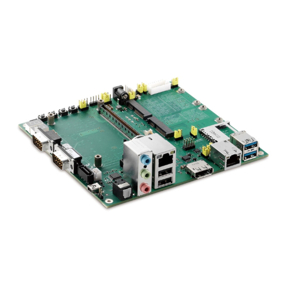
Page 11: Component Locations
3. Component Locations Figure 1: miniBASE-10R Component Locations (See section 8.3 Indicator LEDs on page 34 for detailed LED locations.) Component Locations... - Page 12 This page intentionally left blank. Component Locations...
-
Page 13: Functional Diagram
(9V-12.6V with 3 cell) (2/3 cell) Smart Battery SATA0 BAT2 (5.7-8.4V with 2 cell) SATA (2/3 cell) (9V-12.6V with 3 cell) LVDS Backlight 3.3 or 5V LVDS VDD SDIO / SDIO Fan Power SATA Power Figure 2: miniBASE-10R Functional Block Diagram Functional Diagram... - Page 14 This page intentionally left blank. Functional Diagram...
-
Page 15: Mechanical Drawing
All dimensions are shown in millimeters. Tolerances should be ± 0.25mm, unless otherwise noted.The tolerances on the PCB corner locating peg holes (dimensions [5.08, 5.08], [145.09, 5.08], [5.08, 136.99] and [145.09, 136.99]) should be ± 0.10mm. Figure 3: miniBASE-10R Mechanical Drawing Mechanical Drawing... - Page 16 This page intentionally left blank. Mechanical Drawing...
-
Page 17: Connectors, Pinouts And Jumpers
6. Connectors, Pinouts and Jumpers 6.1. Carrier Board Signals – Type 10 Figure 4: Carrier Board Signals - Type 10 Connectors, Pinouts and Jumpers... -
Page 18: Connector And Pinout Compatibility
10R design and schematics are fully verified, and we recommend that you follow them as a reference for your carrier board design. miniBASE-10R Schematics and Mechanical files as well as the CDG can be downloaded from the miniBASE-10R product webpage: http://www.adlinktech.com/PD/web/PD_detail.php?cKind=&pid=1362... -
Page 19: Com Express Board-To-Board Connectors
6.4. COM Express Board-to-Board Connectors Signals and Pinout comply with COM Express Type 10 B110 A110 COM.0 Type 10 rev. 2.1 Row A Row B GND(FIXED) GND(FIXED) GBE0_MDI3- GBE0_ACT# GBE0_MDI3+ LPC_FRAME# GBE0_LINK100# LPC_AD0 GBE0_LINK1000# LPC_AD1 GBE0_MDI2- LPC_AD2 GBE0_MDI2+ LPC_AD3... - Page 20 SER0_TX DDI0_CTRLCLK_AUX+ SER0_RX DDI0_CTRLDATA_AUX- GND(FIXED) GND(FIXED) SER1_TX / CAN_TX FAN_PWMOUT SER1_RX / CAN_RX FAN_TACHIN LID# SLEEP# VCC_12V VCC_12V VCC_12V VCC_12V VCC_12V VCC_12V VCC_12V VCC_12V VCC_12V VCC_12V VCC_12V VCC_12V GND(FIXED) GND(FIXED) Table 1: miniBASE-10R AB Pin Definitions Connectors, Pinouts and Jumpers...
-
Page 21: Display Connectors
6.5. Display Connectors 6.5.1. JX8: LVDS/eDP Connector For LVDS panel Signal Signal LVDS_A0+ Panel_PWR LVDS_A0- Panel_PWR Panel_EDID_PWR LVDS_A1+ BKLT_PWR LVDS_A1- BKLT_PWR LVDS_A2+ BKLT_CTRL LVDS_A2- BKLT_EN LVDS_A3+ LVDS_A3- LVDS_VDD_EN LVDS_A_CLK+ LVDS_I2C_DATA LVDS_A_CLK- LVDS_I2C_CLK For eDP panel Signal Signal eDP_TX2+ Panel_PWR... - Page 22 6.5.2. JY2: eDP Backlight Voltage Connector Status 5-14V 6.5.3. JX7: DisplayPort Signal Signal (From DDI0 signal on AB connector) Lane0_P Lane0_N Lane1_P Lane1_N Lane2_P Lane2_N Lane3_P Lane3_N CONFIG1 * CONFIG2 * AUX_P AUX_N Hot_Plug RTN_PWR Connectors, Pinouts and Jumpers...
-
Page 23: Lvds Jumper Settings
6.6. LVDS Jumper Settings 6.6.1. JP5: Panel Power Voltage Selects the LVDS Panel Power voltage on JX8 Jumper Status + 3.3V <<<< + 5.0V 6.6.2. JP6: Backlight Power Voltage Selects the Backlight Panel Power voltage on JX8 Jumper Status + 3.3V... -
Page 24: Audio Connectors
6.7. Audio Connectors 6.7.1. JX2: S/PDIF Output Jack (optical) 6.7.2. JX6: S/PDIF Output Header Signal Signal SPDIF - Out 6.7.3. JX1: Three-in-One Audio Phone Jack Color Signal Blue Line-In Green Line-Out Pink MIC-In Connectors, Pinouts and Jumpers... -
Page 25: Mini Pcie And Msata Connector
6.8. Mini PCIe and mSATA Connector 6.8.1. J2: Mini-PCIe Connector Supports Mini-PCIe form factor card Signal Signal Supports PCIe and USB signals WAKE# + 3.3V (from PCIe 0 and USB 4 signals on AB connector) + 1.5V CLKREQ# REFCLK-... - Page 26 6.8.2. J5: Mini-PCIe/mSATA Connector Signal Signal Support Mini-PCIe and mSATA form factor Support PCIe, USB and SATA signal WAKE# + 3.3V (from PCIe 2, USB 5 and SATA 1 signals on AB connector) For Mini-PCIe + 1.5V CLKREQ# REFCLK- REFCLK+ PERST# PERn + 3.3V...
- Page 27 For mSATA Signal Signal WAKE# + 3.3V + 1.5V CLKREQ# REFCLK- REFCLK+ PERST# SATA_RX- + 3.3V SATA_RX+ + 1.5V SMB_CLK SATA_TX- SMB_DATA SATA_TX+ USB_D- USB_D+ + 3.3V + 3.3V PCIe/mSATA_SEL RSVD RSVD + 1.5V RSVD RSVD + 3.3V Connectors, Pinouts and Jumpers...
-
Page 28: Sata
6.8.3. JPX8: Mini-PCIe/mSATA Selection Select the card type for the J5 connector Jumper Status Mini-PCIe <<<< mSATA 6.9. SATA 6.9.1. J9: SATA Drive activity is indicated by LED D3 Signal (see 8.3 Indicator LEDs on page 34) 6.9.2. JX9: Power for SATA Signal + 5.0V Note: <<<<... -
Page 29: Usb And Lan
6.10. USB and LAN 6.10.1. J10: Mini-USB Supports Mini-USB form factor Signal (from USB 7 signals on AB connector) Client_PWR_Dectect USB- USB+ N.C. 6.10.2. J13: USB 3.0 x 2 USB 2.0 compatible (from USB 0, USB_SS0, USB 1, Signal... -
Page 30: Serial Ports
6.10.4. JX3: GbE RJ-45 From GbE signals on AB connector Signal BI_DA+ BI_DA- BI_DB+ BI_DB- BI_DC+ BI_DC- BI_DD+ BI_DD- 6.11. Serial Ports J3: COM 1 J6: COM 2 Signal Signal Only TX/RX support N.C. N.C. N.C. N.C. N.C. N.C. 6.12. C, SMBus and CAN Bus 6.12.1. -
Page 31: Fan Connector
6.12.2. H1: SM Bus Signal + 3.3V SMB_DAT SMB_CLK 6.12.3. JX10: CAN Bus Signal 6.13. Fan Connector 6.13.1. JPX4: Fan Type Selection Selects 4-pin or 3-pin type fan Jumper Status 4P FAN <<<< 3P FAN 6.13.2. JPX5: Fan Control... -
Page 32: Other Connectors
6.14. Other Connectors 6.14.1. JPX6: EXT GPIO Signal Signal GPI_0 GPO_0 Note: address is 42h GPI_1 GPO_1 GPI_2 GPO_2 GPI_3 GPO_3 6.14.2. JPY1: GPIO From GPIO signal on AB connector Signal Signal Note: address is 40h GPI_0 GPO_0 GPI_1 GPO_1 GPI_2 GPO_2 GPI_3... -
Page 33: Other Jumpers
6.14.5. H5: CPLD_JTAG Signal CPLD_TCKL CPLD_TDO + 3.3V CPLD_TMS N.C. N.C. N.C. CPLD_TDI 6.15. Other Jumpers 6.15.1. JP4: Clear CMOS To clear CMOS, shut down the power Signal and short pins 2 and 3 Normal <<<< Clear CMOS 6.15.2. -
Page 34: Power Connectors
6.16. Power Connectors 6.16.1. JX5: AC Adapter For 19V AC adapter (current: 4.7A) 6.16.2. H4/H7: Smart Battery 1/2 Connectors Supports dual Smart Batteries Signal SMBus_Clk SMBus_Dat Thermistor 6.16.3. JPY2: Smart Battery Configuration Select 3-cell or 2-cell battery configuration Signal 3 Cell <<<<... -
Page 35: Power Jumper Settings
6.17. Power Jumper Settings 6.17.1. JPX2: AT/ATX Mode In AT mode, JPX2 shorts PS_ON# to ground directly Signal to force power on. <<<< 6.17.2. JPX3: 5VSB to Module Source Signal w/ 5VSB <<<< w/o 5VSB 6.17.3. JP1: PS_ON# Signal Source... - Page 36 This page intentionally left blank. Connectors, Pinouts and Jumpers...
-
Page 37: Secondary Bios
7. Secondary BIOS The miniBASE-10R supports Secondary BIOS using Serial Peripheral Interface (SPI) for COM.0 Rev. 3.0 modules. Secondary BIOS solutions can be used as an alternative to the on-module BIOS and provide support for the following: • Testing new BIOS versions •... - Page 38 This page intentionally left blank. Secondary BIOS...
-
Page 39: Switches, Post And Leds
8. Switches, POST and LEDs 8.1. Switches (S1-S4) There are four switches on the miniBASE-10R. • S1 switch is the Reset Button. • S2 switch is the Power Button. • S3 switch is the Lid Button. It supports Type 10 modules for ACPI power management behavior setting in OS. -
Page 40: Indicator Leds
8.3. Indicator LEDs There are seven indicator LEDs located on the front side of the board as follows: DZ10 D1: indicates 3.3V power for carrier board D2: indicates 5VSB power for carrier board and COM Express module D3: indicates SATA drive activity (connector J9) D4: indicates 5V power for carrier board D5: indicates 19VDC power adapter is plugged in DZ5: indicates the insertion of WWAN card on mini-PCIe 1 slot... -
Page 41: Smart Battery Management System
3 cells: 9VDC - 12.6VDC Max. Current 4.7A Dependent on battery Power N.A. *Note: The optional reference battery packs provided with miniBASE-10R have 3 cells in series or 2 cells in series. 9.2. Charger Output Capability Charger Voltage 12.6V (3cell) 8.4V (2cell) -
Page 42: Windows Os Interface
9.5. Windows OS Interface 9.5.1. Device Presence ADLINK COM Express Type 10 modules feature a BIOS that fully supports all Smart Battery communications using existing interfaces defined in the COM Express specification and are fully compatible with the integrated Smart Battery Management System. -
Page 43: Safety Instructions
Safety Instructions Read and follow all instructions marked on the product and in the documentation before you operate your system. Retain all safety and operating instructions for future use. • Please read these safety instructions carefully. • Please keep this User‘s Manual for later reference. -
Page 44: Getting Service
5215 Hellyer Avenue, #110, San Jose, CA 95138, USA Tel: +1-408-360-0200 Toll Free: +1-800-966-5200 (USA only) Fax: +1-408-360-0222 Email: info@adlinktech.com ADLINK Technology (China) Co., Ltd. Address: 300 Fang Chun Rd., Zhangjiang Hi-Tech Park, Pudong New Area Shanghai, 201203 China Tel: +86-21-5132-8988 Fax: +86-21-5132-3588 Email: market@adlinktech.com...
Need help?
Do you have a question about the miniBASE-10R and is the answer not in the manual?
Questions and answers