
Subscribe to Our Youtube Channel
Related Manuals for ADLINK Technology Q7-BASE


Summary of Contents for ADLINK Technology Q7-BASE
- Page 1 Q7-BASE Technical Reference Qseven Reference Carrier Board Revision: 3.00 Revision Date: October 03, 2017 Part Number: 50-1Z180-1020 ...
- Page 2 Audience This manual provides reference only for computer design engineers, including but not limited to hardware and software designers and applications engineers. ADLINK Technology, Inc. assumes you are qualified to design and implement prototype computer equipment. Preface...
- Page 3 Q7-BASE Environmental Responsibility ADLINK is committed to fulfill its social responsibility to global environmental preservation through compliance with the European Union's Restriction of Hazardous Substances (RoHS) directive and Waste Electrical and Electronic Equipment (WEEE) directive. Environmental protection is a top priority for ADLINK. We have enforced measures to ensure that our prod- ucts, manufacturing processes, components, and raw materials have as little impact on the environment as possible.
- Page 4 Conventions The following conventions may be used throughout this manual, denoting special levels of information. This information adds clarity or specifics to text and illustrations. This information indicates the possibility of minor physical injury, component damage, data loss, and/or program corruption. This information warns of possible serious physi- cal injury, component damage, data loss, and/or program corruption.
-
Page 5: Table Of Contents
Q7-BASE Table of Contents 1 Product Overview ......................1 Carrier Description ......................... 1 Features..........................2 Ordering Information ......................3 Block Diagram........................3 Specifications......................... 4 1.5.1 Physical ..........................4 1.5.2 Electrical ..........................4 1.5.3 Environmental........................4 1.5.4 Mechanical ........................5 2 Hardware ........................... 7 Interface Headers, Jumper Headers, Switches, LEDs, and Connectors ....... 7 Standard Hardware References .................. - Page 6 3.20 LCD Supply Voltage Select (CN62) ..................30 3.21 ATX PS_ON Selection (CN63).................... 31 3.22 USB0 Voltage Select (CN64) ....................31 3.23 LVDS Backlight (CN65)....................... 31 3.24 LVDS Interface (CN66) ....................... 32 3.25 SIO Enable (CN69) ......................33 3.26 UART Interface (CN70) ....................... 33 3.27 LPT Interface (CN71) ......................
-
Page 7: Product Overview
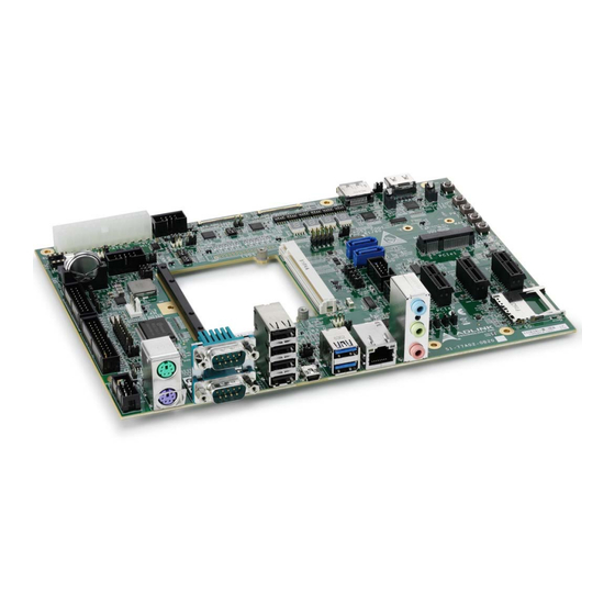
Carrier Specifications Carrier Description The ADLINK Q7-BASE is the host carrier board for ADLINK’s Qseven modules and serves as design reference for systems based on the Qseven form factor. The Qseven module plugs directly into the Q7-BASE, where the carrier board becomes a design platform for testing and developing your applications. -
Page 8: Features
Features Qseven interface MXM connector PCI Express Bus 4x PCIE x1 links 3x PCIE x1 slots 1x PCIE Mini slot Serial Port UART interfaces (2) Null Modem RS-232 on serial ports COM1 / COM2 ... -
Page 9: Ordering Information
Smart Battery RTC Battery Socket Control Buttons and Switches Ordering Information Table 1-1: Q7-BASE Models Model Number Description Qseven Reference Carrier for Qseven compliant modules, featuring Q7-BASE LVDS an MXM2 230-pin module interface with LVDS display support. (91-77A02-000E or higher) -
Page 10: Specifications
Most components on the Q7-BASE carrier are selected as extended temperature range parts (-40°C to +85°C). Some components are not available in this temperature range. In these cases, the component temperature ranges are narrower. The Q7-BASE is validated in the -40°C to +85°C range. -
Page 11: Mechanical
Figure 1-3 provides the mechanical dimensions and mounting hole sizes of the Q7-BASE. The Q7-BASE can be mounted to a chassis using M4, B-head screws. Mezzanine cards can be mounted to the carrier using female-female standoffs with M2.5 threads and M2.5, B-head screws. - Page 12 This page intentionally left blank. Product Overview...
-
Page 13: Hardware
Hardware This chapter describes the physical specifications of the interface connectors, headers, LEDs, and switches on the Q7-BASE. The third section of this chapter further describes the industry standard IO hardware on the carrier. Interface Headers, Jumper Headers, Switches, LEDs, and Connectors... - Page 14 Table 2-1: Header, Connector, Switch, and LED Descriptions (Continued) Header / Signal / Device Description Connector# CN50 " 10-pin, 0.100 (2.54mm) shrouded header for transmitting and receiving Controller Area Network signals [JIHVEI, 23N6960-10S10B-01G-G] CN51 CAN Termination " (2mm) jumper header for terminating the 2-pin, 0.079 CAN interface with 120 ohms [JIH, 21N12050-02S10B-01G-4/2.8-G]...
- Page 15 Q7-BASE Table 2-1: Header, Connector, Switch, and LED Descriptions (Continued) Header / Signal / Device Description Connector# CN75, CN76 PCIe Mini Latch Dual latches for PCIe Mini card socket [ATTEND, 119A-LATCH-80] CN77 CAN Enable 5V " (2mm) jumper header for enabling 5V on 2-pin, 0.079...
- Page 16 Table 2-1: Header, Connector, Switch, and LED Descriptions (Continued) Header / Signal / Device Description Connector# CN96 USB_VBUS Source 3-pin, 2.0mm jumper header for selecting between Select USB_VBUS and USB_CC [JIH21N12050-03S10B-01G-4/2.8-G] CN97 PWM Backlight Voltage 3-pin, 2.0mm jumper header for selecting PWM backlight Select voltage level [JIH21N12050-03S10B-01G-4/2.8-G]...
- Page 17 Q7-BASE Table 2-1: Header, Connector, Switch, and LED Descriptions (Continued) Header / Signal / Device Description Connector# CN114 USB 3.0 OC# Target 3-pin, 2.0mm jumper header for selecting the OC target Select (USB01_OC# or USB67_OC#) [JIH21N12050-03S10B-01G-4/2.8-G] HDMI1 HDMI Interface " (0.50mm) standard connector for HDMI 19-pin, 0.019...
- Page 18 Table 2-1: Header, Connector, Switch, and LED Descriptions (Continued) Header / Signal / Device Description Connector# Reset Button " (4.3mm) push-button switch for asserting 4-pin, 0.170 warm reset to the module [DIPTRONIC, DTSM-61N-V-T] Sleep Button " (4.3mm) push-button switch for asserting 4-pin, 0.170 sleep state to the module [DIPTRONIC, DTSM-61N-V-T]...
- Page 19 Q7-BASE Table 2-1: Header, Connector, Switch, and LED Descriptions (Continued) Header / Signal / Device Description Connector# USB1 USB 2.0 " (3.50mm) quadruple-stacked, standard 16-pin, 0.138 connector for USB 2.0 signals (ports 2, 3, 4, 5) [FOXCONN,UB1112C-QHDF-4F] USB2 Mini USB 2.0 0.80mm standard Mini USB connector for USB...
- Page 20 CONNECTORS: CN91 - HDA_SDI or I2S_SDI Select CN92 - EN_V3P3S Mode Select AJ1 - Audio Jack CN93 - USB3_CN_p or USB3_mPCIe_p Select BT1 - Battery Socket CN94 - USB3_CN_n or USB3_mPCIe_n Select CN1 - ATX Power CN95 - USB OTG Control Select CN2 - Manufacturing CN96 - USB_VBUS Source Select CN3 - BattMan / ATX Power Mode Select...
- Page 21 Q7-BASE Figure 2-3 illustrates the faces of the standard interface connectors mounted along one edge of the carrier. These connectors are for PS1 Keyboard and Mouse, Serial Port, USB, Ethernet, and Audio industry-standard cable connectors. Audio Mini Mouse COM1 (AJ1) 3.0/2.0...
-
Page 22: Standard Hardware References
2.2.1 Audio IO Jack The Q7-BASE provides one standard audio jack for HD audio (AJ1). One audio codec supports this interface. Figure 2-5 depicts the three lines of the audio jacks: Line In (1 - Blue), Line Out (2 - Green), and MIC In (3 - Pink). Figure 2-6 presents the functional block diagram of HDA/I2S sig- nals and hardware on the carrier. -
Page 23: Pcie Mini Card Slot
Q7-BASE 2.2.2 PCIe Mini Card Slot The Q7-BASE is equipped with one PCI Express Mini Card slot (CN74). Figure 2-7 presents the mini card slot with one of the two fastening latches. Figure 2-7: PCIe Mini Card Slot with Latch 2.2.3... -
Page 24: Battery Socket
Table 2-2: SD Card Slot (CN100) Pin # Signal Description Scheme SDIO_D3 SDIO data bit3 SDIO_CMD SDIO Command Ground 3.3V power supply +VCC_SDIO SDIO_CK SDIO clock Ground SDIO_D0 SDIO data bit0 SDIO_D1 SDIO data bit1 SDIO_D2 SDIO data bit2 SDIO_CD# SDIO card detect Ground SDIO_WP... -
Page 25: Interfaces
Q7-BASE Interfaces This chapter provides the pin signals for all the non-standard user interfaces on the Q7-BASE. Unless pinouts for industry standard interfaces have been modified, those pinout tables will not appear in this manual. Signal definitions for standard interfaces such as SATA, USB, and PCIe connectors can be found in their respective specification data sheets. -
Page 26: Manufacturing (Cn2)
Manufacturing (CN2) Table 3-2 lists the pin signals of the Manufacturing header, which provides 6 pins, 2 rows, with odd/even pin sequence (1, 2) and 0.079" (2.00mm) pitch. Table 3-2: Manufacturing (CN2) Pin # Signal Pin # Signal MFG_NC0 (Reserved for MFG_NC1 (Reserved for manufacturing manufacturing and debugging) and debugging) -
Page 27: Smart Battery (Battman) Interface (Cn5)
Q7-BASE Smart Battery (BattMan) Interface (CN5) Table 3-5 lists the pin signals of the Smart Battery header, which provides 10 pins in 2 rows, odd/even pin sequence (1, 2), and 2.54mm pitch. You must configure the jumper settings as described in Table 3-5, or system damage could occur when using a BattMan power supply to Power On the carrier. -
Page 28: Edp Display
Display The following two subsections describe the embedded DisplayPort interface available on the Q7-BASE eDP version of the board. See Figure 3-1 for a display signal map of the Q7-BASE eDP model. Q7-BASE (eDP op on) LVDS 40pin Primary... -
Page 29: Edp1 (Cn11)
Q7-BASE Table 3-7: eDP0 Video Signals (CN10) (Continued) Pin # Signal Description eDP0_LCD_VCC LCD power (3.3V / 5V / 12V) eDP0_LCD_VCC LCD power (3.3V / 5V / 12V) eDP0_HS_GND High-Speed Ground eDP0_AUX_n Auxiliary differential pair - negative eDP0_AUX_p Auxiliary differential pair - positive... -
Page 30: Ps/2 Power Source Select (Cn20)
Table 3-8: eDP1 Video Signals (CN11) (Continued) Pin # Signal Description eDP1_LCD_VCC LCD power (3.3V / 5V / 12V) eDP1_LCD_VCC LCD power (3.3V / 5V / 12V) eDP1_LCD_VCC LCD power (3.3V / 5V / 12V) eDP1_LCD_VCC LCD power (3.3V / 5V / 12V) eDP1_HS_GND High-Speed Ground eDP1_AUX_n... -
Page 31: Com1 / Com2 (Cn39)
Q7-BASE COM1 / COM2 (CN39) This section describes the signals of the dual, standard DB9 serial port connector for RS232 sig- nals. Table 3-10 and Table 3-11 list the pin signals of the 4-wire RS232 interface (COM1 and COM2), which provides a standard dual DB9 connector. -
Page 32: Pci Express X1 (Cn42, Cn44, Cn45)
3.10 PCI Express x1 (CN42, CN44, CN45) Table 3-12 lists the signals for the PCIe A x1 connector, which provides 36 pins, two rows, con- secutive pin sequence (1, 13) with 1.00mm pitch. Table 3-12: PCIe x1 (CN42, CN44, CN45) Signal Signal +V12P0_ATX... -
Page 33: 3.12 Usb Signals
3.12.1 Standard USB Interfaces All USB interfaces on Q7-BASE are supported through standard connectors, and their signal definitions can be found in their respective specification datasheets. Refer to the following block diagram for illustrations of the standard and optional USB interface mappings on the carrier. -
Page 34: Can (Controller Area Network - Cn50)
3.13 CAN (Controller Area Network - CN50) Table 3-14 lists the pin signals of the Controller Area Network interface (CAN), which provides 10 pins in 2 rows, odd/even pin sequence (1, 2), and 2.54mm pitch. Table 3-14: CAN Signals (CN50) Pin # Signal Not Connected... -
Page 35: Cpld Programming (Cn52)
Q7-BASE 3.15 CPLD Programming (CN52) Table 3-16 lists the pin signals of the CPLD Programming header, which provides 10 pins, 2 rows, " pitch. with odd/even sequence and 0.100 (2.54mm) Table 3-16: CPLD Programming Signals (CN52) Pin # Signal POST_TCK (Test Clock) -
Page 36: Backlight Voltage Select (Cn59)
3.18 Backlight Voltage Select (CN59) Table 3-19 lists the pin signals of the Backlight Voltage Select jumper header, which provides " (2mm) pitch. pins, single-row, with 0.079 Table 3-19: Backlight Voltage Select Signals (CN59) Pin # Signal Jumper Position LCD_12V •... -
Page 37: Atx Ps_On Selection (Cn63)
Q7-BASE 3.21 ATX PS_ON Selection (CN63) Table 3-22 lists the pin signals of the ATX PS_ON Selection jumper header, which provides odd/even pin sequence (1, 2) and " (2mm) pitch. pins, 2 rows, with 0.079 Table 3-22: ATX PS_ON Selection (CN63) -
Page 38: Lvds Interface (Cn66)
3.24 LVDS Interface (CN66) This section describes the LVDS interface available on the Q7-BASE LVDS version of the board. See Figure 3-3 for a display signal map of the Q7-BASE LVDS model. Q7-BASE (LVDS op on) LVDS Primary Single/Dual Channel... -
Page 39: Sio Enable (Cn69)
Q7-BASE 3.25 SIO Enable (CN69) Table 3-26 lists the pin signals of the SIO Enable jumper header, which provides 3 pins, single- " (2mm) pitch. Select 1-2 to enable SIO, 2-3 to disable SIO. row, with 0.079 Table 3-26: SIO Enable Signals (CN69) -
Page 40: Lpt Interface (Cn71)
3.27 LPT Interface (CN71) Table 3-28 lists the pin signals of the LPT Interface header, which provides 26 pins, 2 rows, with " pitch. odd/even sequence (1, 2) and 0.100 (2.54mm) Table 3-28: LPT Interface Signals (CN71) Pin # Signal Pin # Signal LPT_STB#_R... -
Page 41: Can 5-Volt Enable (Cn77)
Q7-BASE 3.29 CAN 5-Volt Enable (CN77) Table 3-30 lists the pin signals of the CAN 5-Volt Enable jumper header, which provides 2 pins " (2mm) pitch. The jumper header enables an additional 5 volts and ground for the with 0.079 CAN header at CN50, pin 9. -
Page 42: Usb1 Voltage Select (Cn80)
3.32 USB1 Voltage Select (CN80) Table 3-33 lists the pin signals of the USB1 Voltage Select jumper header, which provides 3 pins, " (2mm) pitch. single-row, with 0.079 Table 3-33: USB1 Voltage Select Signals (CN80) Pin # Signal +V5P0_SBY +VCC_USB2345PWR +V5_IN NOTE: The shaded table cells denote Ground or Power. -
Page 43: Display Mode Select (Cn85)
Q7-BASE Table 3-35: DisplayPort Signals (CN84) (Continued) Pin # Signal Description +3V3S_DP DisplayPort Power NOTE: The shaded table cells denote power or ground. 3.35 Display Mode Select (CN85) Table 3-36 lists the pin signals of the Display Mode Select jumper header, which provides 3 pins in a single row with 2.00mm pitch. -
Page 44: Hda_Rst# / I2S_Rst# Select (Cn88)
3.38 HDA_RST# / I2S_RST# Select (CN88) Table 3-39 lists the pin signals of the HDA_RST# / I2S_RST# Select jumper header, which pro- vides 3 pins in a single row with 2.00mm pitch. Table 3-39: HDA_RST# / I2S_RST# Select (CN88) Pin # Signal Jumper Position I2S_RST#... -
Page 45: V3P3S Select (Cn92)
Q7-BASE 3.42 EN_V3P3S Select (CN92) Table 3-43 lists the pin signals of the EN_V3P3S Select jumper header, which provides 3 pins in a single row with 2.00mm pitch. Table 3-43: EN_V3P3S Select (CN92) Pin # Signal Jumper Position +V5_IN • Jumper Installed 1-2 - ATX mode •... -
Page 46: Usb_Vbus Source Select (Cn96)
3.46 USB_VBUS Source Select (CN96) Table 3-47 lists the pin signals of the USB_VBUS Source Select jumper header, which provides 3 pins in a single row with 2.00mm pitch. Table 3-47: USB_VBUS Source Select (CN96) Pin # Signal Jumper Position USB_VBUS_SRC •... -
Page 47: I2C Eeprom Address Select Switch (Sw6)
Q7-BASE 3.50 I2C EEPROM Address Select Switch (SW6) Table 3-51 lists the pin signals of the I2C EEPROM address select dip switch, which provides 4 poles, 8 positions with 1.27mm pitch. Table 3-51: I2C EEPROM Address Select Switch (SW6) Pin #... -
Page 48: Dp Enable Switch (Sw12)
3.53 DP Enable Switch (SW12) Table 3-54 lists the pin signals of the DP Enable dip switch, which provides 4 poles, 8 positions with 1.27mm pitch. Table 3-54: DP Enable Switch (SW12) Pin # Signal Pin# Signal 1 (off) DP_ENABLE [Default] 8 (on) 2 (off) DP_AUTOEQ [Default]... -
Page 49: Edp0 Control Switch (Sw16)
Q7-BASE 3.56 eDP0 Control Switch (SW16) Table 3-57 lists the pin signals of the eDP0 Control dip switch, which provides 4 poles, 8 posi- tions with 1.27mm pitch. Table 3-57: eDP0 Control Switch (SW16) Pin # Signal Pin# Signal 1 (off) -
Page 50: Edp1 Control Switch (Sw19)
3.59 eDP1 Control Switch (SW19) Table 3-60 lists the pin signals of the eDP1 Control dip switch, which provides 4 poles, 8 posi- tions with 1.27mm pitch. Table 3-60: eDP1 Control Switch (SW19) Pin # Signal Pin# Signal 1 (off) eDP1_CNTRL [Default] 8 (on) +V3P3S... -
Page 51: Appendix A Technical Support
Q7-BASE Appendix A Technical Support ADLINK Technology, Inc. provides a number of methods for contacting Technical Support listed in Table A-1 below. Requests for support through Ask an Expert are given the highest priorities, and usually will be addressed within one working day. - Page 52 Table A-1: Technical Support Contact Information (Continued) Method Contact Information LiPPERT ADLINK Technology GmbH Address: Hans-Thoma-Strasse 11 D-68163 Mannheim, Germany Tel: +49-621-43214-0 Fax: +49-621 43214-30 Email: emea@adlinktech.com Please visit Contact page at www.adlinktech.com for information on how to contact the ADLINK regional office nearest you.
Need help?
Do you have a question about the Q7-BASE and is the answer not in the manual?
Questions and answers