Table of Contents
Advertisement
Quick Links
Advertisement
Table of Contents

Subscribe to Our Youtube Channel
Related Manuals for Neoway N27


Summary of Contents for Neoway N27
- Page 1 Hardware User Guide Issue 2.0 Date 2021-10-15...
- Page 2 THIS GUIDE PROVIDES INSTRUCTIONS FOR CUSTOMERS TO DESIGN THEIR APPLICATIONS. PLEASE FOLLOW THE RULES AND PARAMETERS IN THIS GUIDE TO DESIGN AND COMMISSION. NEOWAY WILL NOT TAKE ANY RESPONSIBILITY OF BODILY HURT OR ASSET LOSS CAUSED BY IMPROPER OPERATIONS. THE INFORMATION IN THIS DOCUMENT IS SUBJECT TO CHANGE WITHOUT NOTICE DUE TO PRODUCT VERSION UPDATE OR OTHER REASONS.
-
Page 3: Table Of Contents
5.2 Temperature Features ........................ 46 5.3 ESD Protection ........................... 46 6 RF Features ................... 47 6.1 Operating Bands ........................47 6.2 TX Power and RX Sensitivity ..................... 48 6.3 GNSS Feature ..........................51 Copyright © Neoway Technology Co., Ltd. All rights reserved. - Page 4 7.2 Label ............................52 7.3 Packing ............................53 7.3.1 Packaging .......................... 53 7.3.2 Moisture ..........................54 8 Mounting N27 onto Application PCB ............55 8.1 Bottom Dimensions ........................55 8.2 Application Foot Print ......................... 56 8.3 Stencil ............................56 8.4 Solder Paste ..........................56 8.5 SMT Furnace Temperature Curve ....................
- Page 5 Figure 4-21 GNSS RF structure ....................... 39 Figure 4-22 Specifications of MM9329-2700RA1 ................40 Figure 4-23 RF connections ......................40 Figure 4-24 Antenna layout ......................41 Figure 4-25 Layout around the antenna ................... 41 Copyright © Neoway Technology Co., Ltd. All rights reserved.
- Page 6 Figure 7-1 N27 dimensions (Unit: mm) .................... 52 Figure 8-1 Bottom dimensions of N27 (Unit: mm) ................55 Figure 8-2 Recommended footprint of N27 application PCB (Unit: mm) ......... 56 Figure 8-3 SMT furnace temperature curve ..................57 Copyright © Neoway Technology Co., Ltd. All rights reserved.
- Page 7 Table 6-3 RX sensitivity of N27 GSM ....................49 Table 6-4 RX sensitivity of N27 Cat M1 ................... 49 Table 6-5 RX sensitivity of N27 Cat NB1 (without retransmission) ..........50 Table 6-6 RX sensitivity of N27 Cat NB1 (with retransmission) ............50...
- Page 8 About This Document Scope This document is applicable to N27 series. It defines the features, indicators, and test standards of the N27 module and provides reference for the hardware design of each interface. Audience This document is intended for system engineers (SEs), development engineers, and test engineers.
- Page 9 If these points are not followed, the module or user device may fail. Indicates instructions or tips. This symbol provides advices or suggestions that may be useful when using the module. Related Documents Neoway_N27_Datasheet Neoway_N27_Product_Specifications Neoway_N27_AT_Command_Mannual Neoway_N27_EVK_User_Guide Copyright © Neoway Technology Co., Ltd. All rights reserved.
-
Page 10: Safety Recommendations
Follow the requirements below during the application design and use of this product: Do not disassemble this product without permission from Neoway. Otherwise, we are entitled to refuse to provide further warranty. Design your application correctly based on the hardware user guide. Connect this product to a stable power supply and route traces following fire safety standards. -
Page 11: About N27
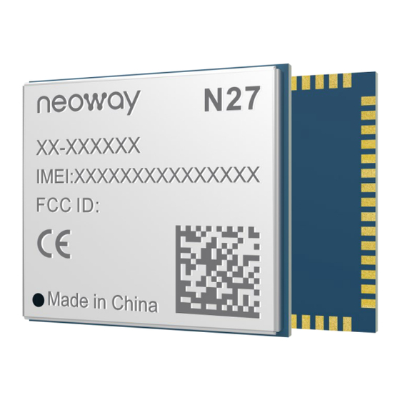
B20, B25, B26, B28, B66, B71, B85 GPRS: 850/900/1800/1900 MHz N27 adopts a 76-pin package with a square GND pad at each corner. Its dimensions are only 24.0 mm × 18.0 mm × 2.3 mm. With industrial-grade performance, it is well applicable to electrical terminals, tracker, POS, and other IoT terminals. -
Page 12: Basic Features
* indicates that the function is in the development phase. 2.3 Basic Features Parameter Description Dimensions: (24.0± 0.15) mm × (18.0± 0.15) mm × (2.3± 0.2) mm Physical features Package: LGA Weight: 2.4g Copyright © Neoway Technology Co., Ltd. All rights reserved. - Page 13 PDU, TXT Protocol TCP, UDP, HTTP, FTP, MQTT, LWM2M, COAP Certification approval European Union: CE/RoHS/POPs Some RF indicators might not meet 3GPP/3GPP2 standards in extended temperature but it does not affect functioning. Copyright © Neoway Technology Co., Ltd. All rights reserved.
- Page 14 N27 Hardware User Guide Chapter 2 About N27 U.S.: FCC/PTCRB/AT&T Japan: JATE Australia: RCM Europe: GCF Deutsche Telekom Copyright © Neoway Technology Co., Ltd. All rights reserved.
-
Page 15: Module Pins
N27 Hardware User Guide Chapter 3 Module Pins 3 Module Pins There are 76 pins on N27 and their pads are introduced in the LGA package. 3.1 Pad Layout Figure 3-1 shows the pad layout of the N27. The superscript indicates that the pin is defined to be supported by the open version. -
Page 16: Pin Description
1, 4, 10, 22, 32, 46, 58, 60, 67, 70, 72, 73, 74, Ensure that all GND pins are 75, 76 connected to the ground plane Control Interfaces ON/OFF Connected to 1.8V through an PWRKEY_N button internal pull-up resistor Copyright © Neoway Technology Co., Ltd. All rights reserved. - Page 17 Leave this pin floating if it is not used. Software (open) version: used Request as UART1_RTS and used for UART1_RTS send data transmission and log printing. Leave this pin floating Copyright © Neoway Technology Co., Ltd. All rights reserved.
- Page 18 Leave the UART2_RXD Data RX pins floating. SIM Interface card Support 1.8V only, Omax USIM_VCC power supply =30mA output card Connect USIM_VCC USIM_DATA through 10 kΩ pull-up data IO Copyright © Neoway Technology Co., Ltd. All rights reserved.
- Page 19 I2C Interface Software (open) version: used as I2C2_SCL. Connect it to I2C2_SCL I2C clock 1.8V by using an external 2.2 kΩ pull-up resistor. Leave this pin floating if it is not used. Copyright © Neoway Technology Co., Ltd. All rights reserved.
- Page 20 SPI4_MISO. Slave input, Software (open) version: used SPI4_MOSI master as SPI4_MOSI. output Software (open) version: used SPI4_CS_N Chip select as SPI4_CS_0. GPIO GPIO_31 GPIO_32 GPIO_33 GPIO_34 GPIO_35 GPIO_36 With interrupt Copyright © Neoway Technology Co., Ltd. All rights reserved.
- Page 21 Do not pull up these pins to high level or ground them before the module is started completely. otherwise, the module cannot start up successfully. Copyright © Neoway Technology Co., Ltd. All rights reserved.
-
Page 22: Application Interfaces
Ensure low resistance of power supply trace in design to avoid voltage drop. Never use a diode to make the drop voltage between a higher input and module power. Otherwise, Neoway will not provide a warranty for product issues caused by this. In this situation, the diode will obviously decrease the module performances, or result in unexpected restarts, due to the forward voltage of the diode will vary greatly in different temperature and current. -
Page 23: Figure 4-1 Recommended Power Design
The trace should be 3 mm in width at least and the ground plane should be as complete as possible. The traces of the power circuit should be as short and wide as possible. Copyright © Neoway Technology Co., Ltd. All rights reserved. -
Page 24: Vddio_1P8
Connect GND pins and bottom pads to the ground to optimize heat sink and separate noise. 4.1.2 VDDIO_1P8 N27 provides one VDDIO_1P8 pin that outputs 1.8V@50mA. VDDIO_1P8 is enabled automatically when the module is awake or in a running state. -
Page 25: Figure 4-3 Reference Design Of Startup Controlled By Mcu
UART Shutdown Process The N27 module allows users to shut it down through hardware or software. PWRKEY_N is used to power the module off. When the module is working, inputting negative pulse for longer than 2 seconds to PWRKEY_N can trigger the shutdown process of the module. -
Page 26: Peripheral Interfaces
AIO USB data negative signal USB2.0 used to download the module firmware USB_DP AIO USB data positive signal The N27 module can be used as a USB device. It is an option for customers. Copyright © Neoway Technology Co., Ltd. All rights reserved. -
Page 27: Uart
Keep the trace of USB_VBUS wider than 0.3 mm. 4.3.2 UART Signal Function Remarks Software (open) version: used as UART0_TXD Data TX UART1_TXD. UART0_RXD Data RX Software (open) version: used as Copyright © Neoway Technology Co., Ltd. All rights reserved. -
Page 28: Figure 4-7 Uart Connection
Note the match of signals. The UART of N27 operates in a power domain of 1.8V. If your host MCU is not in this power domain, add a level shifting circuit between the module and the host. The following figure shows the... -
Page 29: Sim
Surround the traces with the ground plane if possible. 4.3.3 SIM Signal Function Remarks USIM_VCC USIM power output 1.8V only USIM_DATA USIM data IO USIM_CLK USIM clock USIM_RESET USIM reset USIM_DET USIM detection A pull-up resistor is recommended. Copyright © Neoway Technology Co., Ltd. All rights reserved. -
Page 30: Figure 4-9 Reference Design Of The Sim Card Interface
USIM_PRESENT in series to enhance the ESD performance. N27 supports SIM card detect, but this function is determined by the structure of the SIM card connector. The module determines the SIM card status based on the level of the USIM_PRESENT pin. -
Page 31: Pcm
Software (open) version: PCM_DOUT PCM data signal output Do not use this pin. Leave this pin floating. N27 provides one PCM interface that operates at 1.8V. Figure 4-10 shows the reference design of the PCM interface. Figure 4-10 PCM connection PCM_DOUT PCM_DIN... -
Page 32: Figure 4-11 Pcm Sync Signal Timing
Table 4-1 Timing parameters of PCM interface Timing Parameter Minimum Value Typical Value Maximum Value Unit μs t(sync) PCM_SYNC cycle PCM_SYNC valid t(synca) time PCM_SYNC invalid μs t(syncd) 124.5 time t(clk) PCM_CLK cycle t(clkh) PCM_CLK high time Copyright © Neoway Technology Co., Ltd. All rights reserved. - Page 33 Delay time from PCM_CLK t(zdout) PCM_DOUT high impedance N27 provides one I2S interface, which is multiplexed from PCM. It operates at 1.8 V and can be used for digital audio. Signal Function Remarks I2S_MCLK I2S main clock Max. frequency: 12.288MHz...
-
Page 34: Figure 4-14 I2S Connection
Table 4-2 Timing parameters of I2S interface Timing Parameter Minimum Value Typical Value Maximum Value Unit Clock cycle 81.380 t(HC) Clock high time 0.45*T 0.55*T t(LC) Clock low time 0.45*T 0.55*T Copyright © Neoway Technology Co., Ltd. All rights reserved. -
Page 35: Spi
The SPI interface supports 1.8 V and only master mode. The following figures show the SPI connection and timing. Figure 4-16 SPI connection SPI_MISO SPI_MISO SPI_MOSI SPI_MOSI SPI_CS_N SPI_CLK N27 module SPI device (host) (device) Copyright © Neoway Technology Co., Ltd. All rights reserved. -
Page 36: I2C
2.2 kΩ pull-up resistor. Leave this pin floating if it is not used. N27 provides one standard I2C interface, which supports master mode only. The interface complies with I2C Specification, version 5.0, October 2012. I2C operates at 1.8V and does not embed an internal pull-up resistor. It is recommended to connect it to 1.8V or VDDIO_1P8 through a 2.2 kΩ... -
Page 37: Rf Interface
GNSS antenna 4.4.1 ANT Interface ANT of N27 requires a characteristic impedance of 50 Ω. You should control the impedance of the traces between the pins and antenna to ensure the RF performance. An impedance matching circuit, such as the L network, split capacitor network, and pi network is mandatory in between. Pi network is recommended. -
Page 38: Figure 4-19 Pi Network
Lay copper foil around the RF connector. Dig as many ground holes as possible on the copper to ensure the lowest grounding impedance. Keep the trace between N27 and the antenna connector as short as possible. Control the trace impedance to 50Ω. ... -
Page 39: Ant_Gnss Interface
4.4.2 ANT_GNSS Interface GPS Impedance Control ANT_GNSS (71st pin) is the GNSS RF interface of N27, which requires a characteristic impedance of 50Ω. Figure 4-21 shows the GNSS structure inside the module. Figure 4-21 GNSS RF structure... -
Page 40: Antenna Assembling
The following methods are commonly used to assemble antenna: GSC RF connector MM9329-2700RA1 from Murata is recommended. The following figure shows its encapsulation specifications. Figure 4-22 Specifications of MM9329-2700RA1 Figure 4-23 RF connections PCB Printing or SMT Copyright © Neoway Technology Co., Ltd. All rights reserved. -
Page 41: Figure 4-24 Antenna Layout
5 Space between the antenna and ground area. Figure 4-25 shows the layout of this area. Figure 4-25 Layout around the antenna For more details, refer to the antenna manuals and other documents. Copyright © Neoway Technology Co., Ltd. All rights reserved. -
Page 42: Gpio Interfaces
With interrupt GPIO_46. Software (open) version: Do not use this GPIO_45 pin. Leave this pin floating. Software (open) version: Do not use this GPIO_47 With interrupt pin. Leave this pin floating. Copyright © Neoway Technology Co., Ltd. All rights reserved. -
Page 43: Other Interfaces
Add an ESD component to protect USB_BOOT. Figure 4-26 Reference design of USB_BOOT VDDIP_1P8 10kΩ USB_BOOT 4.6.3 STATUS This pin outputs 1.8V high level to control the startup indicator after the module is started successfully. Copyright © Neoway Technology Co., Ltd. All rights reserved. -
Page 44: Net_Light
N27 Hardware User Guide Chapter 4 Application Interfaces 4.6.4 NET_LIGHT NET_LIGHT outputs a continuous pulse signal after the module registers with the network. For details about the light modes, see Neoway_N27_AT_Command_Manual. Copyright © Neoway Technology Co., Ltd. All rights reserved. -
Page 45: Electric Features And Reliability
N27 Hardware User Guide Chapter 5 Electric Features and Reliability 5 Electric Features and Reliability This chapter describes the electric feature and reliability of the N27 module. 5.1 Electric Features Table 5-1 Operating conditions of N27 Parameter Minimum Value Typical Value Maximum Value 3.1V... -
Page 46: Temperature Features
± 8KV ± 15KV Cover ± 8KV ± 15KV Others ± 2KV ± 4KV Some RF indicators might not meet 3GPP/3GPP2 standards in extended temperature but it does not affect functioning. Copyright © Neoway Technology Co., Ltd. All rights reserved. -
Page 47: Rf Features
FDD-LTE B25 1850~1915MHz 1930~1995MHz FDD-LTE B26 814~849MHz 859~894MHz FDD-LTE B27 (CATM-only) 807~824MHz 852~869MHz FDD-LTE B28 703~748MHz 758~803MHz FDD-LTE B31 452.5~457.5MHz 462.5~467.5MHz FDD-LTE B66 1710~1780MHz 2110~2180MHz FDD-LTE B71 (CATNB only) 617~652MHz 663~698MHz Copyright © Neoway Technology Co., Ltd. All rights reserved. -
Page 48: Tx Power And Rx Sensitivity
23dBm+2/-2dB(CATNB) HD-FDD LTE B31 23dBm+2/-2dB <-40 dBm HD-FDD LTE B66 23dBm+2/-2dB <-40 dBm HD-FDD LTE B71 (CATNB only) 20dBm+2/-2dB <-40 dBm HD-FDD LTE B72 23dBm+2/-2dB <-40dBm HD-FDD LTE B73 23dBm+2/-2dB <-40dBm Copyright © Neoway Technology Co., Ltd. All rights reserved. -
Page 49: Table 6-3 Rx Sensitivity Of N27 Gsm
HD-FDD LTE B85 23dBm+2/-2dB <-40 dBm Table 6-3 RX sensitivity of N27 GSM Band Sensitivity ≤-108dBm@200KHz EGSM800/900 ≤-108dBm@200KHz DCS1800/1900 Table 6-4 RX sensitivity of N27 Cat M1 Band Sensitivity (dBm/1.08M) Duplex Mode ≤-107 LTE B1 HD-FDD ≤-107 LTE B2 HD-FDD ≤-107... -
Page 50: Table 6-5 Rx Sensitivity Of N27 Cat Nb1 (Without Retransmission)
N27 Hardware User Guide Chapter 6 RF Features All values above were obtained in the lab. In actual applications, there might be a difference because of network environments. Table 6-5 RX sensitivity of N27 Cat NB1 (without retransmission) Band Sensitivity(dBm/180KHz) Duplex Mode ≤-114... -
Page 51: Gnss Feature
TBD (CEP50) Hot start (in air) Cold start (in air) Update frequency 1Hz by default CNRin/CNRout Max. positioning altitude Max. positioning speed Max. positioning acceleration GNSS data type GNSS antenna type Passive Copyright © Neoway Technology Co., Ltd. All rights reserved. -
Page 52: Mechanical Features
N27 Hardware User Guide Chapter 7 Mechanical Features 7 Mechanical Features This chapter describes the mechanical features of N27. 7.1 Dimensions Figure 7-1 dimensions (Unit: mm) 7.2 Label The label information is curved on the shell. Copyright © Neoway Technology Co., Ltd. All rights reserved. -
Page 53: Packing
The material and surface finishing must comply with RoHS directives. 7.3 Packing N27 modules are packed in sealed bags on delivery to guarantee a long shelf life. Follow the same package of the modules again in case of opened for any reason. -
Page 54: Moisture
Chapter 7 Mechanical Features 7.3.2 Moisture N27 is a level 3 moisture-sensitive electronic elements, in compliance with IPC/JEDEC J-STD-020 standard. If the module is exposed to air for more than 48 hours at conditions not worse than 30° C/60% RH, bake it at a temperature higher than 90 degrees for more than 12 hours before SMT. -
Page 55: Mounting N27 Onto Application Pcb
Chapter 8 Mounting N27 onto Application PCB 8 Mounting N27 onto Application PCB N27 is introduced in a 76-pin LGA package. This chapter describes the N27 footprint, recommended PCB design and SMT information to guide users on how to mount the module onto the application PCB board. -
Page 56: Application Foot Print
N27 Hardware User Guide Chapter 8 Mounting N27 onto Application PCB 8.2 Application Foot Print Figure 8-2 Recommended footprint of N27 application PCB (Unit: mm) 8.3 Stencil The recommended stencil thickness is at least 0.15 mm to 0.20 mm. 8.4 Solder Paste Do not use the kind of solder paste different from our module technique. -
Page 57: Smt Furnace Temperature Curve
Chapter 8 Mounting N27 onto Application PCB 8.5 SMT Furnace Temperature Curve Neoway will not provide a warranty for heat-responsive element abnormalities caused by improper temperature control. Thin or long PCB might bend during SMT. So, use loading tools during the SMT and reflow soldering process to avoid poor solder joint caused by PCB bending. - Page 58 Chapter 8 Mounting N27 onto Application PCB melt. Then remove the module using tweezers. Do not shake the module in high temperatures while removing it. Otherwise, the components inside the module might get misplaced. Copyright © Neoway Technology Co., Ltd. All rights reserved.
-
Page 59: Abbreviations
Frequency Division Multiple Access Full Rate GPRS General Packet Radio Service Global Standard for Mobile Communications Half Rate Integrated Circuit IMEI International Mobile Equipment Identity Liquid Crystal Display Light Emitting Diode Copyright © Neoway Technology Co., Ltd. All rights reserved. - Page 60 Subscriber Identification Module Short Message Service SRAM Static Random Access Memory Terminal adapter TDMA Time Division Multiple Access UART Universal Asynchronous Receiver-Transmitter USSD Unstructured Supplementary Service Data VSWR Voltage Standing Wave Ratio Copyright © Neoway Technology Co., Ltd. All rights reserved.
Need help?
Do you have a question about the N27 and is the answer not in the manual?
Questions and answers