Table of Contents
Advertisement
SERVICE MANUAL
Main Section
I Specifications
I Preparation for Servicing
I Adjustment Procedures
I Schematic Diagrams
I CBA's
I Exploded Views
I Parts List
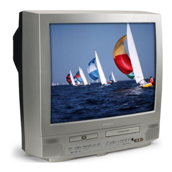
27" ANALOG/DIGITAL
PURE FLAT COLOR TV/DVD/VCR
CT270MW8
When servicing the deck
mechanism, refer to MK14 Deck
Mechanism Section.
Deck Mechanism Part No.:
N2466FT
Advertisement
Table of Contents

Related Manuals for Magnavox CT270MW8


Summary of Contents for Magnavox CT270MW8
- Page 1 When servicing the deck I Specifications mechanism, refer to MK14 Deck I Preparation for Servicing Mechanism Section. I Adjustment Procedures I Schematic Diagrams Deck Mechanism Part No.: I CBA’s I Exploded Views N2466FT I Parts List 27″ ANALOG/DIGITAL PURE FLAT COLOR TV/DVD/VCR CT270MW8...
- Page 2 IMPORTANT SAFETY NOTICE Proper service and repair is important to the safe, reliable operation of all Funai Equipment. The service procedures recommended by Funai and described in this service manual are effective methods of performing service operations. Some of these service special tools should be used when and as recommended.
-
Page 3: Table Of Contents
MAIN SECTION 27″ ANALOG/DIGITAL PURE FLAT COLOR TV/DVD/VCR CT270MW8 Main Section I Specifications I Preparation for Servicing I Adjustment Procedures I Schematic Diagrams I CBA’s I Exploded Views I Parts List TABLE OF CONTENTS Specifications ................1-1-1 Laser Beam Safety Precautions . -
Page 4: Specifications
SPECIFICATIONS *ˆ Mode---------SP mode unless otherwise specified * Test input terminal <Except Tuner>--------Video input (1 Vp-p) Audio input (-10 dB) <Tuner>------------------Ant. input (80 dBµV) Video: 87.5% Audio: 25 kHz dev. (1 kHz Sin) < DEFLECTION > Description Condition Unit Nominal Limit 1. - Page 5 < VCR > Description Condition Unit Nominal Limit 1. Horizontal Resolution (R/P, SP) Line µs 2. Jitter (Low) (R/P, SP) AM(SP) (R/P, SP) 3. S/N Chroma PM(SP) (R/P, SP) 4. Wow & Flutter (JIS, UNWTD) (R/P, SP) 0.25 < TUNER > Description Condition Unit...
- Page 6 < ATSC > Description Condition Unit Nominal Limit >100 1. RECEIVED FREQ. RANGE (-28dBm) – >100 2. ATSC DYNAMIC RANGE (min./max.) VHF LOW BAND. CH.4 dBµV 26/114 32/108 VHF HI BAND. CH.10 dBµV 26/114 32/108 UHF BAND. CH.41 dBµV 28/118 34/112 3.
-
Page 7: Laser Beam Safety Precautions
LASER BEAM SAFETY PRECAUTIONS This DVD player uses a pickup that emits a laser beam. Do not look directly at the laser beam coming from the pickup or allow it to strike against your skin. The laser beam is emitted from the location shown in the figure. When checking the laser diode, be sure to keep your eyes at least 30 cm away from the pickup lens when the diode is turned on. -
Page 8: Important Safety Precautions
IMPORTANT SAFETY PRECAUTIONS Prior to shipment from the factory, our products are strictly inspected for recognized product safety and electrical codes of the countries in which they are to be sold. However, in order to maintain such compliance, it is equally important to implement the following precautions when a set is being serviced. - Page 9 Also, because the picture tube shields and an isolation transformer only if the AC power mounting hardware perform an X-radiation plug is inserted so that the chassis is protection function, they must be correctly in connected to the ground side of the AC power place.
- Page 10 of the countries in which they are to be sold. 2) Strip about 15 mm of the insulation from the However, in order to maintain such compliance, it ends of the wires. If the wires are stranded, is equally important to implement the following twist the strands to avoid frayed conductors.
- Page 11 Safety Check after Servicing Examine the area surrounding the repaired location for damage or deterioration. Observe that screws, parts and wires have been returned to original positions. Afterwards, perform the following tests and confirm the specified values in order to verify compliance with safety standards. 1.
-
Page 12: Standard Notes For Servicing
STANDARD NOTES FOR SERVICING Circuit Board Indications Pb (Lead) Free Solder 1. The output pin of the 3 pin Regulator ICs is Pb free mark will be found on PCBs which use Pb indicated as shown. free solder. (Refer to figure.) For PCBs with Pb free mark, be sure to use Pb free solder. - Page 13 around the flat pack-IC to protect other parts from With Soldering Iron: damage. (Fig. S-1-2) 1. Using desoldering braid, remove the solder from 3. The flat pack-IC on the CBA is affixed with glue, so all pins of the flat pack-IC. When you use solder be careful not to break or damage the foil of each flux which is applied to all pins of the flat pack-IC, pin or the solder lands under the IC when...
- Page 14 2. Installation With Iron Wire: 1. Using desoldering braid, remove the solder from 1. Using desoldering braid, remove the solder from all pins of the flat pack-IC. When you use solder the foil of each pin of the flat pack-IC on the CBA flux which is applied to all pins of the flat pack-IC, so you can install a replacement flat pack-IC more you can remove it easily.
- Page 15 Instructions for Handling Semi- conductors Electrostatic breakdown of the semi-conductors may occur due to a potential difference caused by electrostatic charge during unpacking or repair work. 1. Ground for Human Body Be sure to wear a grounding band (1 MΩ) that is properly grounded to remove any static electricity that may be charged on the body.
-
Page 16: Preparation For Servicing
PREPARATION FOR SERVICING How to Enter Service Mode Adjustment Mode Caution 1: YUV Brightness up adjustment mode in DTV mode: 1. Optical sensors system are used for Tape Start See adjustment instructions. and End Sensor on this equipment. Read this page carefully and prepare as described on this Purity check mode: page before starting to service;... -
Page 17: Cabinet Disassembly Instructions
CABINET DISASSEMBLY INSTRUCTIONS 1. Disassembly Flowchart Removal Step/ This flowchart indicates the disassembly steps for the Remove/*Unhook/ Loc. Part Fig. Unlock/Release/ cabinet parts, and the CBA in order to gain access to Note Unplug/Unclamp/ item(s) to be serviced. When reassembling, follow the Desolder steps in reverse order. - Page 18 Reference Notes in the Table 1) Disconnect Connector (CN301) on the DVD Main CBA Unit. CAUTION! 2) Short the three short lands of FPC cable with When removing the CRT, be sure to discharge the solder before removing the FFC cable (CN201) Anode Lead of the CRT with the CRT Ground Wire from it.
- Page 19 [2] Tray Chassis Unit (S-8) (S-5) Top Shield (S-5) [4] DVD (S-8) Mechanism (S-9) (S-9) [5] DVD Main (S-9) [8] Deck CBA Unit Assembly (S-13) (S-13) (S-6) (S-12) (S-6) [10] Digital (S-6) CBA Unit (S-7) (S-6) [6] Sub CBA [7] Function [9] Main CBA (S-10) (S-12)
- Page 20 Anode Cap CRT CBA (S-4) (S-4) (S-4) [3] CRT (S-4) Fig. D3 DVD Mechanism Short the three short lands by soldering. (Either of two places.) View for A FPC Cable Fig. D4 1-6-4 T3200DC...
- Page 21 DVD MAIN CBA UNIT DVD MAIN CBA UNIT CN301 CN301 CN201 CN201 JUNCTION-B JUNCTION-B TO SPEAKER TO SPEAKER CN2A CN2A CN1A CN1A CL3801 CL3801 ANODE ANODE CN3801 CN3801 CN2801 CN2801 CN2571 CN2571 CL2501A CL2501A SUB CBA SUB CBA CL2504A CL2504A CN2 CN1 CN2 CN1 FOCUS...
-
Page 22: Electrical Adjustment Instructions
ELECTRICAL ADJUSTMENT INSTRUCTIONS General Note: “CBA” is abbreviation for How to enter Service mode: “Circuit Board Assembly.” Service mode: Note: Electrical adjustments are required after 1. Use the service remote control unit. replacing circuit components and certain mechanical parts. It is important to perform 2. - Page 23 2. Setting for CONTRAST, COLOR, YC-COLOR (YC-COL) 1. Press [2] button to select “YC-COLOR (YC-COL)” TINT, V-TINT and SHARPNESS display. Data Values 2. Press [CH. o/p] buttons so that the value of “YC- COLOR (YC-COL)” becomes “58”. <TV mode (Composite block)> 1.
- Page 24 3. C-Trap Adjustment 4. H f Adjustment Purpose: To get minimum leakage of the color signal Purpose: To get correct horizontal position and size of carrier. screen image. Symptom of Misadjustment: If C-Trap Adjustment is Symptom of Misadjustment: Horizontal position and incorrect, stripes will appear on the screen.
- Page 25 5. Cut-off/Drive Adjustment 6. H. Size Adjustment Purpose: To obtain correct size of screen image. Purpose: To adjust the beam current of R, G, B, and Symptom of Misadjustment: Size of screen image screen voltage. may not be properly displayed. Symptom of Misadjustment: White color may be reddish, greenish or bluish.
- Page 26 8. White Balance Adjustment 9. Sub-Brightness Adjustment Purpose: To mix red, green and blue beams correctly Purpose: To get proper brightness. for pure white. Symptom of Misadjustment: If Sub-Brightness is Symptom of Misadjustment: White becomes bluish incorrect, proper brightness cannot be obtained by or reddish.
- Page 27 11. H. Position Adjustment 12. V. Position Adjustment Purpose: To obtain correct horizontal position of Purpose: To obtain correct vertical position of screen screen image. image. Symptom of Misadjustment: H. position may not be Symptom of Misadjustment: If V. position is properly displayed.
- Page 28 14. Head Switching Position The following 2 adjustments normally are not attempted in the field. They should be done only Adjustment when replacing the CRT then adjust as a preparation. Purpose: Determine the Head Switching Position during Playback. 15. Purity Adjustment Symptom of Misadjustment: May cause Head Purpose: To obtain pure color.
- Page 29 16. Convergence Adjustment 4. Fix the C.P. Magnets by tightening the Ring Lock. 5. Remove the DY Wedges and slightly tilt the Purpose: To obtain proper convergence of red, green Deflection Yoke horizontally and vertically to and blue beams. obtain the best overall convergence. Symptom of Misadjustment: If Convergence 6.
-
Page 30: How To Initialize The Tv/Dvd/Vcr
HOW TO INITIALIZE THE TV/DVD/VCR To put the program back at the factory-default, initialize the TV/DVD/VCR as the following procedure. < DVD Section > < TV/VCR Section > 1. Turn the power on and press [SELECT] button on 1. Use the service remote control unit. the remote control unit to put the TV/DVD/VCR 2. -
Page 31: Firmware Renewal Mode
FIRMWARE RENEWAL MODE 1. Turn the power on and press [SELECT] button on " ******* " differs depending on the models. the remote control unit to put the TV/DVD/VCR into DVD mode. Then remove the disc on the tray. F/W Version Up Mode Model No : ******* (It is possible to move to F/W version up mode VERSION : *.**... -
Page 32: Block Diagrams
BLOCK DIAGRAMS < TV/VCR Section > System Control / Servo Block Diagram 1-10-1 T3251BLS... - Page 33 Video Block Diagram 1-10-2 T3251BLV...
- Page 34 Audio Block Diagram 1-10-3 T3251BLA...
- Page 35 Hi-Fi Audio Block Diagram 1-10-4 T3251BLH...
- Page 36 TV Process Block Diagram 1-10-5 T3251BLT...
- Page 37 Digital Tuner Block Diagram 1-10-6 T3251BLDT...
- Page 38 CRT/H.V. Block Diagram 1-10-7 T3251BLCRT...
- Page 39 Power Supply Block Diagram 1-10-8 T3251BLP...
- Page 40 BLOCK DIAGRAMS < DVD Section > DVD System Control / Servo Block Diagram 1-10-9 T3251BLSD...
- Page 41 Digital Signal Process Block Diagram 1-10-10 T3251BLD...
-
Page 42: Schematic Diagrams / Cba's And Test Points
SCHEMATIC DIAGRAMS / CBA’S AND TEST POINTS Standard Notes WARNING Many electrical and mechanical parts in this chassis have special characteristics. These characteristics often pass unnoticed and the protection afforded by them cannot necessarily be obtained by using replacement components rated for higher voltage, wattage, etc. - Page 43 LIST OF CAUTION, NOTES, AND SYMBOLS USED IN THE SCHEMATIC DIAGRAMS ON THE FOLLOWING PAGES: 1. CAUTION: FOR CONTINUED PROTECTION AGAINST RISK OF FIRE, REPLACE ONLY WITH SAME TYPE_A,_V FUSE. ATTENTION: UTILISER UN FUSIBLE DE RECHANGE DE MÊME TYPE DE_A,_V. 2.
- Page 44 Main 1/6 & Sensor Schematic Diagram < TV/VCR Section > T3251SCM1 1-11-3...
- Page 45 Main 2/6 Schematic Diagram < TV/VCR Section > T3251SCM2 1-11-4...
- Page 46 Main 3/6 Schematic Diagram < TV/VCR Section > T3251SCM3 1-11-5...
- Page 47 Main 4/6 Schematic Diagram < TV/VCR Section > 1-11-6 T3251SCM4...
- Page 48 Main 5/6 & Junction-A Schematic Diagram < TV/VCR Section > T3251SCM5 1-11-7...
- Page 49 Main 6/6 Schematic Diagram < TV/VCR Section > VOLTAGE CHART (Power off mode) Ref. No. IC1601 25.7 24.7 CAUTION ! Ref. No. Fixed voltage (or Auto voltage selectable) power supply circuit is used in this unit. IC1682 CAUTION ! : For continued protection against risk of fire, If Main Fuse (F1601) is blown , check to see that all components in the power supply Ref.
- Page 50 Sub 1/3 Schematic Diagram < TV/VCR Section > 1-11-9 T3251SCSUB1...
- Page 51 Sub 2/3 Schematic Diagram < TV/VCR Section > T3251SCSUB2 1-11-10...
- Page 52 Sub 3/3 Schematic Diagram < TV/VCR Section > 1-11-11 T3251SCSUB3...
- Page 53 CRT Schematic Diagram < TV/VCR Section > T3251SCCRT Function & Junction-B Schematic Diagram < TV/VCR Section > T3251SCF 1-11-12...
- Page 54 Digital 1/3 Schematic Diagram < TV/VCR Section > 1 NOTE: The order of pins shown in this diagram is different from that of actual IC101. IC101 is divided into two and shown as IC101 (1/2) ~ IC101 (2/2) in this Digital Schematic Diagram Section. VOLTAGE CHART CN101 Pin No.
- Page 55 Digital 2/3 Schematic Diagram < TV/VCR Section > T3251SCD2 1-11-14...
- Page 56 Digital 3/3 Schematic Diagram < TV/VCR Section > 1 NOTE: The order of pins shown in this diagram is different from that of actual IC101. IC101 is divided into two and shown as IC101 (1/2) ~ IC101 (2/2) in this Digital Schematic Diagram Section. T3251SCD3 1-11-15...
- Page 57 DVD Main 1/3 Schematic Diagram < DVD Section > 1-11-16 T3251SCDT1...
- Page 58 DVD Main 2/3 Schematic Diagram < DVD Section > T3251SCDT2 1-11-17...
- Page 59 DVD Main 3/3 Schematic Diagram < DVD Section > 1-11-18 T3251SCDT3...
- Page 60 Main CBA Top View < TV/VCR Section > CAUTION ! Because a hot chassis ground is present in the power Fixed voltage (or Auto voltage selectable) power supply circuit is used in this unit. CAUTION ! : For continued protection against risk of fire, supply circuit, an isolation transformer must be used.
- Page 61 Main CBA Bottom View < TV/VCR Section > CAUTION ! Because a hot chassis ground is present in the power CAUTION ! : For continued protection against risk of fire, Fixed voltage (or Auto voltage selectable) power supply circuit is used in this unit. supply circuit, an isolation transformer must be used.
- Page 62 Sub CBA Top View < TV/VCR Section > TP2501 TP1301 B-OUT TP2504 VR2531 H SIZE VR2530 PIN.C R2583 (H f Adjustment) 1-11-21 BT3221F01023-A...
- Page 63 Sub CBA Bottom View < TV/VCR Section > WF17 PIN 8 OF CN2 WF18 PIN 6 OF CN2 WF19 PIN 4 OF CN2 WF20 PIN 1 OF CN2 TP2503 H-DRIVE WF11 PIN 5 OF CN2571 WF10 Q2571 Collector BT3221F01023-A 1-11-22...
- Page 64 CRT CBA Top View < TV/VCR Section > CRT CBA Bottom View < TV/VCR Section > WF14 WF13 WF12 Q2501 Q2502 Q2503 Collector Collector Collector BT3221F01023-B 1-11-23...
- Page 65 Junction-A CBA Function CBA Top View < TV/VCR Section > Junction-A CBA Top View Bottom View < TV/VCR Section > < TV/VCR Section > BT3221F01023-D Junction-B CBA Junction-B CBA Top View Bottom View < TV/VCR Section > < TV/VCR Section > Function CBA Bottom View <...
-
Page 66: Waveforms
WAVEFORMS T3200WF 1-12-1... - Page 67 1-12-2 T3200WF...
-
Page 68: Wiring Diagram
WIRING DIAGRAM < TV/VCR Section > T3251WIT 1-13-1... - Page 69 WIRING DIAGRAM < DVD Section > T3251WID 1-13-2...
-
Page 70: System Control Timing Charts
SYSTEM CONTROL TIMING CHARTS < TV/VCR Section > Mode SW: LD-SW LD-SW Position detection A/D Input voltage Limit Symbol (Calculated voltage) 3.76 V ~ 4.50 V (4.12 V) 4.51 V ~ 5.00 V (5.00 V) 0.00 V ~ 0.25 V (0.00 V) 1.06 V ~ 1.50 V (1.21 V) 0.66 V ~ 1.05 V (0.91 V) 1.99 V ~ 2.60 V (2.17 V) - Page 71 Chart 1 1) SP MODE 18 RF-SW The first rise of RF-SW after a rise in F-AD signal. F-AD ( Internal Signal ) "H" "H" "Z" C-DRIVE Stop Detection Acceleration Detection Slow Tracking Value PB CTL Reversal Limit Value 66 C-F/R ROLL COMPENSATION (DRUM SERVO)
- Page 72 Chart 2 2) LP/EP MODE 18 RF-SW The first rise of RF-SW after a rise in F-AD signal. F-AD ( Internal Signal ) "H" "H" "Z" C-DRIVE Stop Detection Acceleration Detection Slow Tracking Value PB CTL Reversal Limit Value 66 C-F/R ROLL COMPENSATION (DRUM SERVO)
- Page 73 Chart 3 EJECT ST-S/ END-S "OFF" CASS.LOAD LD-FWD 0.2S LD-REV SFT-SW STOP(B) POWER LD-FWD 0.4S 0.2S LD-REV 0.2S LD-FWD 0.5S LD-REV STOP(A) PLAY LD-FWD PLAY LD-FWD RS1(RS2) LD-REV 0.2S LD-FWD FS1(FS2) PLAY PLAY PAUSE (SLOW) LD-FWD STILL(SLOW) PLAY LD-REV 0.2S LD-FWD PLAY STOP...
- Page 74 Chart 4 STOP(A) STOP LD-REV 0.2S LD-FWD 0.2S STOP /EJECT 1.0S LD-FWD 0.5S LD-REV STOP(A) LD-REV 0.2S LD-FWD 0.2S STOP /EJECT LD-REV 1.0S LD-FWD 0.5S LD-REV STOP(A) LD-FWD PAUSE LD-FWD 2.5S Short REV LD-REV 0.2S LD-FWD REC PAUSE REC or PAUSE STOP /EJECT...
- Page 75 < DVD Section > Tray Close ~ Play / Play ~ Tray Open Tray Disc Disc Tray Play Close Rotation Stop Open 3.3V Tray IN (TL221) Sled Drive 1.65V (TP303) Disc Drive 1.65V (TP301) 1.65V Focus Drive (TP304) Tracking Drive 1.65V (TP302) 1-14-6...
-
Page 76: Ic Pin Function Descriptions
IC PIN FUNCTION DESCRIPTIONS IC1201 (TV/VCR Micro Controller IC) Signal Function Name “H” ≥ 4.5 V, “L” ≤ 1.0 V 30 OUT DTV-H DTV On Signal at High Signal 31 OUT P-ON-H Power On Signal at High Function Name 32 OUT BUS-CONT Bus Control IN LD-SW Loading Switch Input REC-... - Page 77 Signal Signal Function Function Name Name 64 OUT OSD-R Red Signal Output Record/Playback Control CTL (+) Signal (+) DTV-S- 65 OUT DTV Serial Data Output SOUT AMPC Amp Capacitor IN DTV-S-SIN DTV Serial Data Input CTL-AMP- 97 OUT Control Amp Output DTV-S- 67 OUT DTV Serial Clock...
-
Page 78: Lead Identifications
LEAD IDENTIFICATIONS MID-32A22F 2SK3407(F) 2SC2785(F,J) 2SA1175(F) 2SA950-O(TE2 F T) KRA103M-AT/P 2SC2120-O(TE2 F T) KRC103M-AT/P 2SC1627-Y(TE2.F.T) KTC3199-GR-AT/P 2SC3331(T) KTC3199-Y-AT/P 2SC3708S 2SD400(F) G D S E C B E C B AN17812A LA78041-E 2SD1666R 2SC5360 FA Q TLV1117IDCYRG3 1: GND 2: Vout 3: Vin 1 2 3 B C E... -
Page 79: Exploded Views
EXPLODED VIEWS Cabinet SHINWHA TAPE SGT-730 (BLACK) Details for L551 V501-2 and surrounding parts SHINWHA TAPE SGT-730 V501-1 (WHITE) L551 TB18 L3-1 DVD Mechanical Parts Scotch Tape #880 CRT CBA CLN551 CLN551 CLN551 L3-2 TL1-1 TL1-1 DVD Main Scotch CBA Unit TL1-2 Tape #880 TL1-1... - Page 80 Packing Tape Packing Tape 1-17-2 T3251PEX...
-
Page 81: Mechanical Parts List
FRONT CABINET T3251UB 1EM021666 V501# CRT A68QBT892X TCRT190SM028 A1-2 CONTROL PLATE T3251UB 1EM221542 V501-1 PCM JH88DTA XM04000BV010 A1-3 BADGE BRAND T7310UL ~MAGNAVOX~ 0EM407275 CRT TYPE B A1-4 CASSETTE DOOR T3251UB 1EM424230 A1-5 SPRING DOOR T1200UA 1EM422903 L551# DEFLECTION YOKE 6150Z-1046A LLBY00ZGS008 A1-6 CLOTH(4X7XT0.7) T5000UA... -
Page 82: Electrical Parts List
ELECTRICAL PARTS LIST PRODUCT SAFETY NOTE: Products marked with a Ref. No. Description Part No. # have special characteristics important to safety. C1050 CHIP CERAMIC CAP . CH D 6pF/50V CHD1JD3CH6R0 Before replacing any of these components, read C1121 CHIP CERAMIC CAP . CH J 220pF/50V CHD1JJ3CH221 carefully the product safety notice in this service C1122... - Page 83 Ref. No. Description Part No. Ref. No. Description Part No. C1424 CHIP CERAMIC CAP . F Z 1µF/10V CHD1AZ30F105 C1766 ELECTROLYTIC CAP . 2.2µF/50V M H7 CE1JMAVSL2R2 C1425 CHIP CERAMIC CAP . F Z 1µF/10V CHD1AZ30F105 C1769 ELECTROLYTIC CAP . 22µF/16V M H7 CE1CMAVSL220 C1426 ELECTROLYTIC CAP .
- Page 84 Ref. No. Description Part No. Ref. No. Description Part No. CN601B TERMINAL PRINTBORD PIN MS-PIN155155 JTEA001CHY01 D1685# SWITCHING DIODE 1SS133(T-77) QDTZ001SS133 CN1103 BOARD CONNECTOR 19P(PB FREE) JCTWA19TG004 D1687# SWITCHING DIODE 1SS133(T-77) QDTZ001SS133 127301119K2 D1688# SWITCHING DIODE 1SS133(T-77) QDTZ001SS133 CN1104 TWG CONNECTOR 07P TWG-P07P-A1 J3TWA07TG001 D1689# SWITCHING DIODE 1SS133(T-77)
- Page 85 Ref. No. Description Part No. Ref. No. Description Part No. CARBON RES. 1/4W J 1.5 Ω Q1208 TRANSISTOR 2SC2785(F) QQSF02SC2785 R1146 RCX4JATZ01R5 CARBON RES. 1/2W J 2.2 Ω Q1209 TRANSISTOR 2SC2785(F) QQSF02SC2785 R1147 RCX2JZQZ02R2 CARBON RES. 1/4W J 1.2 Ω Q1210 TRANSISTOR 2SC2785(F) QQSF02SC2785...
- Page 86 Ref. No. Description Part No. Ref. No. Description Part No. CHIP RES. 1/10W J 100k Ω CHIP RES. 1/10W J 220 Ω R1231 RRXAJR5Z0104 R1417 RRXAJR5Z0221 CHIP RES. 1/10W J 6.8k Ω CHIP RES. 1/10W J 330 Ω R1232 RRXAJR5Z0682 R1418 RRXAJR5Z0331 CHIP RES.
- Page 87 Ref. No. Description Part No. Ref. No. Description Part No. CARBON RES. 1/4W J 5.6 Ω R1691 RCX4JATZ05R6 R1906 PCB JUMPER D0.6-P5.0 JW5.0T CARBON RES. 1/2W J 18 Ω CARBON RES. 1/4W J 1.2k Ω R1692 RCX2JZQZ0180 R1907 RCX4JATZ0122 CARBON RES. 1/2W J 18 Ω CHIP RES.
- Page 88 Ref. No. Description Part No. Ref. No. Description Part No. TP1202 PCB JUMPER D0.6-P18.0 JW18.0T C2534# P .P .CAP 0.027µF/630V J CBP2KKD00273 TP1401 PCB JUMPER D0.6-P24.0 JW24.0T C2535# ALMINIUM ELECTRIC CAPACITOR CA1J4R7NC235 UHA1H4R7KHD TP1402 PCB JUMPER D0.6-P22.0 JW22.0T C2536 FILM CAP .(P) 0.1µF/50V J CMA1JJS00104 TP1403 PCB JUMPER D0.6-P22.0...
- Page 89 Ref. No. Description Part No. Ref. No. Description Part No. CHIP RES. 1/10W J 15k Ω D2584 SWITCHING DIODE 1SS133(T-77) QDTZ001SS133 R2319 RRXAJR5Z0153 CARBON RES. 1/4W J 470 Ω D2585 ZENER DIODE MTZJT-775.1B QDTB0MTZJ5R1 R2321 RCX4JATZ0471 CARBON RES. 1/4W J 15 Ω D2586 PCB JUMPER D0.6-P5.0 JW5.0T...
- Page 90 Ref. No. Description Part No. Ref. No. Description Part No. CHIP RES. 1/10W J 10k Ω R2582 RRXAJR5Z0103 TP1301 PCB JUMPER D0.6-P10.0 JW10.0T METAL OXIDE FILM RES. 2W J 1.8 Ω R2583# RN021R8ZU001 TP1302 PCB JUMPER D0.6-P7.5 JW7.5T CARBON RES. 1/4W J 1k Ω R2584 RCX4JATZ0102 TP1303...
- Page 91 FUNCTION CBA Ref. No. Description Part No. FUNCTION CBA (MPS-C) ---------- Consists of the following: CONNECTORS CN2401 BOARD CONNECTOR 07P(PB FREE) JCTWA07TG004 127301107K2 CN2801 242 SERIES CONNECTOR 224202104W1 J322C04TG001 RESISTORS CHIP RES. 1/10W F 1.5k Ω R2401 RRXAFR5Z1501 CHIP RES. 1/10W F 1.5k Ω R2402 RRXAFR5Z1501 CHIP RES.(1608) 1/10W F 2.2k Ω...
- Page 92 Misuse of any trademarks or any other content in this manual is strictly prohibited. Funai shall aggressively enforce its intellectual property rights to the fullest extent of the law. CT270MW8 T3251UB 2007-01-25...
Need help?
Do you have a question about the CT270MW8 and is the answer not in the manual?
Questions and answers