Table of Contents
Advertisement
Quick Links
Product Variants
Model
OBU-301E(v2)
V2X On-Board Unit, V2Xcast
OBU-301U(v2)
V2X On-Board Unit, V2Xcast
OBU-351
V2X On-Board Unit, 0A1/0A2
OBU-351E
V2X On-Board Unit, V2Xcast
OBU-351U
V2X On-Board Unit, V2Xcast
EVK-351
V2X Starter Kit, 0A1/0A2
EVK-351E
V2X Starter Kit, V2Xcast
EVK-351U
V2X Starter Kit, V2Xcast
Reviewers
Department
Name
PD
Nidor Huang
RD
JY Ou
Modification History
Revision
Date
0.1
2021/08/23
0.2
2021/10/13
A printed version of this document is an uncontrolled copy
© 2021 Unex Technology Corporation – Company Confidential
Quick Start Guide
for
OBU-300 Family
®
- C-V2X stack, Europe, 0A1/0A2
®
- C-V2X stack, USA, 0A1/0A2
Acceptance Date
2021/10/13
2021/10/13
Originator
Nidor Huang
Creating document
Adding product variants
Adding product characteristics
Nidor Huang
Adding dimensions and weight
Adding EVK package content
Doc. No: Unex-QSG-21-001
Document Number
Revision
Authors
Description
®
- ITS-G5 stack, 0A1/0A2
- WAVE stack, 0A1/0A2
®
- C-V2X stack, Europe, 0A1/0A2
®
®
- C-V2X stack, USA, 0A1/0A2
Note
Comment
Unex-QSG-21-001
0.2
Nidor Huang
1/27
Advertisement
Table of Contents

Related Manuals for Unex OBU-300


Summary of Contents for Unex OBU-300
- Page 1 Nidor Huang Creating document Adding product variants Adding product characteristics 2021/10/13 Nidor Huang Adding dimensions and weight Adding EVK package content 1/27 A printed version of this document is an uncontrolled copy © 2021 Unex Technology Corporation – Company Confidential...
-
Page 2: Table Of Contents
Figure 7: Ethernet port ......................13 Figure 8: I/O port (J8) ......................13 Figure 9: I/O port cable connector ................... 14 2/27 A printed version of this document is an uncontrolled copy © 2021 Unex Technology Corporation – Company Confidential... - Page 3 Table 14: SW2 and SW3 functions ..................20 Table 15: Console pinout (CN4) ....................21 Table 16: Ext GNSS pinout (CN6) ................... 22 3/27 A printed version of this document is an uncontrolled copy © 2021 Unex Technology Corporation – Company Confidential...
- Page 4 Table 19: USB1 pinout (CN2) ....................24 Table 20: GPIO pinout (J1) ...................... 24 Table 21: Dimensions and weight .................... 26 Table 22: Unex BSP interface settings ..................27 4/27 A printed version of this document is an uncontrolled copy...
-
Page 5: Objective
Customer's sole and exclusive remedy and the entire liability of Unex under this limited warranty will be, at Unex's option, return for repair to Unex's repair center with freight and insurance prepaid or shipment of a replacement within the warranty period or a refund of the purchase price if the hardware is returned to Unex. -
Page 6: Safety Guidelines
• The photos shown in this document may seem different from actual product. However, the differences do not affect actual functionalities. 6/27 A printed version of this document is an uncontrolled copy © 2021 Unex Technology Corporation – Company Confidential... -
Page 7: Figure 1: Obu-301(V2)/Obu-351 Series Package Content
Doc. No: Unex-QSG-21-001 Figure 1: OBU-301(v2)/OBU-351 series package content Figure 2: EVK-301(v2)/EVK-351 series package content 7/27 A printed version of this document is an uncontrolled copy © 2021 Unex Technology Corporation – Company Confidential... -
Page 8: Functional Block Diagram
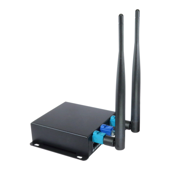
Doc. No: Unex-QSG-21-001 Figure 3: OBU-301(v2)/OBU-351 series complete assembly appearance 6. Functional Block Diagram Figure 4: Functional block diagram 8/27 A printed version of this document is an uncontrolled copy © 2021 Unex Technology Corporation – Company Confidential... -
Page 9: Electrical Characteristics
Conditions Min. Typ. Max. Unit Ta (Ambient operating temperature) Free-air temp. °C USB0 Vbus Supply voltage POWER USB1_Vbus output Vbus voltage 9/27 A printed version of this document is an uncontrolled copy © 2021 Unex Technology Corporation – Company Confidential... - Page 10 *2: TRIGGER_SW (SW3.2) = ON *3: TRIGGER_SW (SW3.2) = OFF *4: IOL = 10 mA, IOH = -10mA *5: RX (J8.3) / EXT_GNSS_TX (J8.14) 10/27 A printed version of this document is an uncontrolled copy © 2021 Unex Technology Corporation – Company Confidential...
-
Page 11: Power Consumption
*3: TX @ 100% duty cycle (CH172, 20dBm) 8. I/O Interfaces 8.1. OBU-301(v2)/OBU-351 8.1.1. External Interfaces 8.1.1.1. LED Figure 5: LED 11/27 A printed version of this document is an uncontrolled copy © 2021 Unex Technology Corporation – Company Confidential... -
Page 12: Figure 6: Usb0 (Cn2)
The power input/output is determined by the hardware design of the OTG cable. However, setting of the USB mode and detection of external device should be implemented by the user. 12/27 A printed version of this document is an uncontrolled copy © 2021 Unex Technology Corporation – Company Confidential... -
Page 13: Figure 7: Ethernet Port
9: I/O IGURE PORT CABLE CONNECTOR A cable assembly with 24AWG wire should be used to connect to vehicular wire harnesses. 13/27 A printed version of this document is an uncontrolled copy © 2021 Unex Technology Corporation – Company Confidential... -
Page 14: Figure 9: I/O Port Cable Connector
GPIO2 Female Connector Female Connector Female Terminal JST 20CPT-B-2A (Rear) JST 20CPT-B-2A (Front) JST SCPT-A021GF-0.5 Figure 9: I/O port cable connector 14/27 A printed version of this document is an uncontrolled copy © 2021 Unex Technology Corporation – Company Confidential... -
Page 15: Internal Interfaces
A USB 2.0 device with mini PCIe form factor can be connected to the mini PCIe port (J6). However please note that although the form factor is mini PCIe, the PCI Express interface is not available. 15/27 A printed version of this document is an uncontrolled copy © 2021 Unex Technology Corporation – Company Confidential... -
Page 16: Figure 12: Mini Pcie Port (J6)
Not connected J6.8 UIM PWR 3.0/1.8 SIM card power J6.10 UIM_DATA 3.0/1.8 SIM card data J6.12 UIM_CLK 3.0/1.8 SIM card clock 16/27 A printed version of this document is an uncontrolled copy © 2021 Unex Technology Corporation – Company Confidential... -
Page 17: Figure 13: Sim Slot (J7)
The SIM slot has a metal flip lid. It is necessary to slide the lid into “Unlock” position before open it. Lock Unlock Open Figure 13: SIM slot (J7) 17/27 A printed version of this document is an uncontrolled copy © 2021 Unex Technology Corporation – Company Confidential... -
Page 18: Figure 14: Tamper Input (J5)
The trigger mode of tamper detection signal can be selected with the DIP switch SW3.2. 18/27 A printed version of this document is an uncontrolled copy © 2021 Unex Technology Corporation – Company Confidential... -
Page 19: Figure 15: Sar Adc Input (J4)
ADC signal, ADC signal wires can be soldered directly into PTHs. (Wires with JST 5P- SZN 1.5mm pitch board-in connector can be handled more easily when soldering.) 19/27 A printed version of this document is an uncontrolled copy © 2021 Unex Technology Corporation – Company Confidential... -
Page 20: I/O Conversion Board (Evk-351 Series Only)
(EX-46) should be connected between EVK-351 and EX-47. The EX-46 and EX-47 are not included in OBU-301(v2)/OBU-351 package and should be ordered separately if needed. 20/27 A printed version of this document is an uncontrolled copy © 2021 Unex Technology Corporation – Company Confidential... -
Page 21: Console
Not Connected CN4.9 Not Connected Console is a RS232 DCE (Data Communication Equipment). 8.2.2. Ext GNSS Figure 19: Ext GNSS port (CN6) 21/27 A printed version of this document is an uncontrolled copy © 2021 Unex Technology Corporation – Company Confidential... -
Page 22: Can0
Ext GNSS is a RS232 DTE (Data Terminal Equipment). If an external GNSS source can output NMEA sentences over RS232, this is to port to connect. Please note that software integration of GNSS protocol will be needed for proper functionality. Contact Unex representative for more detail. -
Page 23: Can1
(total 120 Ω) are added to CAN1 port. If jumper caps are removed, the termination resistors are disconnected. Figure 23: CAN1 terminator jumpers (JP3/JP4) 23/27 A printed version of this document is an uncontrolled copy © 2021 Unex Technology Corporation – Company Confidential... -
Page 24: Usb1
Figure 25: GPIO headers (J1) Table 20: GPIO pinout (J1) Symbol Level (V) Description J1.1 GPIO1 GPIO1 J1.2 Ground J1.3 GPIO2 GPIO2 J1.4 Ground 24/27 A printed version of this document is an uncontrolled copy © 2021 Unex Technology Corporation – Company Confidential... -
Page 25: Dc Power Jack
Input power range is DC 6-48V. Suggested power is 12W or higher. 8.2.8. Reset Button Figure 27: Reset button Pushing the reset button can reboot Linux system. 25/27 A printed version of this document is an uncontrolled copy © 2021 Unex Technology Corporation – Company Confidential... -
Page 26: Dimensions And Weight
Figure 29: Mechanical dimensions - FRONT Table 21: Dimensions and weight Model Length (mm) Width (mm) Height (mm) Weight (g) OBU-301(v2) 95.0 103.0 31.2 152.6 OBU-351 26/27 A printed version of this document is an uncontrolled copy © 2021 Unex Technology Corporation – Company Confidential... -
Page 27: Software Settings
Doc. No: Unex-QSG-21-001 10. Software Settings The following BSP settings are applicable for Unex software package only. Table 22: Unex BSP interface settings Function Description Console RS232, 115200bps, 8N1, ttyAMA2 EXT GNSS RS232, 230400bps, 8N1, ttyAMA1 (GPIO100=0) GNSS NMEA UART1, 230400bps, 8N1, ttyAMA1 (GPIO100=1) GNSS Debug (Opt.)
Need help?
Do you have a question about the OBU-300 and is the answer not in the manual?
Questions and answers