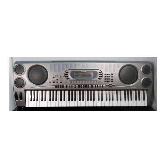
Casio WK-1800 Service Manual
Hide thumbs
Also See for WK-1800:
- User manual (96 pages) ,
- User manual (46 pages) ,
- User manual (47 pages)
Advertisement
INDEX
WK-1800
MAY.2000
FULL RANGE
CHORD
MAX
FINGERED
CASIO CHORD
MIN
EXTERNAL
CH 1
CH 2
CH 3
CH 4
CH 5
SONG
PATTERN
INTERNAL
UPPER1
UPPER2
LOWER1
LOWER2
ACC VOL.
BANK
HIGH-GRADE KEYBOARD
7
8
9
4
5
6
1
2
3
/NO
/YESS
CH 6
CH 7
CH 8
CH 9
CH 10
CH 11
CH 12
CH 13
CH 14
CH 15
CH 16
PARAMETER RESET:
0
MAIN MANU/
DELETE
CHANNEL VOLUME:
CHORD1
CHORD2
CHORD3
BASS
RHYTHM
TR1
TR2
TR3
TR4
TR5
TR6
SUB MANU/
CHANNEL SELECT:
STORE
AMP ENVELOPE
DECAY
SUSTAIN
PITCH ENVELOPE
00 FLAT
01-17 VIBRATO
18-45 OTHERS
WK-1800
Ver.1 : Apr. 2007
Advertisement
Table of Contents

Related Manuals for Casio WK-1800


Summary of Contents for Casio WK-1800
- Page 1 WK-1800 MAY.2000 AMP ENVELOPE DECAY FULL RANGE CHORD SUSTAIN FINGERED PITCH ENVELOPE CASIO CHORD 00 FLAT 01-17 VIBRATO /YESS 18-45 OTHERS EXTERNAL CH 1 CH 2 CH 3 CH 4 CH 5 CH 6 CH 7 CH 8 CH 9...
-
Page 2: Table Of Contents
CONTENTS Specifications ---------------------------------------------------------------------------------------------- 2 Important Operation ------------------------------------------------------------------------------------- 4 Block Diagram --------------------------------------------------------------------------------------------- 5 Circuit Description --------------------------------------------------------------------------------------- 6 Diagnostic Program ------------------------------------------------------------------------------------ 22 Major Waveformes -------------------------------------------------------------------------------------- 28 Printed Circuit Board ---------------------------------------------------------------------------------- 29 Exploded View ------------------------------------------------------------------------------------------- 34 Parts List --------------------------------------------------------------------------------------------------- 35 Schematic Diagrams ----------------------------------------------------------------------------------- 38 —... -
Page 3: Specifications
Auto accompaniment Rhythm patterns: 130 (120 + 10 user rhythms) Tempo: Variable (226 steps, = 30 to 255) Chords: 3 fingering methods (CASIO CHORD, FINGERED, FULL RANGE CHORD) Rhythm controller: Start/Stop, Intro, Normal/Normal Fill-In, Variation/Variation Fill-In, Synchro/Ending Accomp volume: 0 to 127 (128 steps) - Page 4 Other functions Pitch bend range: Adjustable (12 semitones upwards and downwards) Modulation: Equipped Transpose: 25 steps (–12 semitones to +12 semitones) Adjustable (A4 = approximately 440Hz ± 50 cents) Tuning: Terminals MIDI terminal: IN, OUT Sustain/Assignable jack: Standard jack (sustain, sostenuto, soft, rhythm start/stop) Line out L(MONO)/R Output Impedance: 3 kΩ...
-
Page 5: Important Operation
IMPORTANT OPERATION Full Initialization Use this procedure to return all keyboard settings to what they were when you purchased it. Note that this procedure clears all data from memory. • While holding down the ENTER button, turn on keyboard power. R e s e t ? •... -
Page 6: Block Diagram
BLOCK DIAGRAM Keyboard SEG1 ~ SEG40 MIDI LCD Driver SED1278F2A SI0 ~ Back Light Back Light Driver FI0 ~ LSI601 COM1 ~ COM16 TE-CFL733-IMI Q601, Q602 Key Controller LDB4 TC190C020AF-001 ~LDB7 LSI6 LEDCK, LEDCL LEDs S-Register CONT, RESB TC74HC164 LEDA ~ LEDH LRS, ROM2 ROM1... -
Page 7: Circuit Description
CIRCUIT DESCRIPTION KEY MATRIX F#11 G#11 A#11 F#12 G#12 A#12 C#21 D#21 F#21 C#22 D#22 F#22 G#21 A#21 C#31 G#22 A#22 C#32 D#31 F#31 G#31 A#31 D#32 F#32 G#32 A#32 C#41 D#41 F#41 C#42 D#42 F#42 G#41 A#41 C#51 G#42 A#42 C#52 D#51... - Page 8 /YES CH12 STOP CON- ACC VOL TEMPO STORE TRAST CH13 FREE TRANSPOSE TEMPO CHORD1 SESSION CH14 ONE TOUCH CHORD2 TRANSPOSE BANK DISK CH15 PRESET PWSW POWER LED MATRIX LED-A LED-B LED-C FULL RANGE FINGERD CASIO CHORD CHORD — 7 —...
- Page 9 MEMORY DEVICES Each memory device has the following data. 1 RAM1 : RAM1 S-RAM for operation program, Register, Pattern, Song and SMF data from FDD. (Lower part of data bus) 1 Mbit LSI7 2 RAM2 : Internal Memory S-RAM for operation program, Register, Pattern, Song 512 kbit RAM2 and SMF data from FDD.
- Page 10 POWER SUPPLY CIRCUIT The power supply circuit provides various voltages as shown below. The voltage VDD (+5 V) is provided as long as batteries or AC adaptor is set. Other voltages are controlled by APO (Auto Power Off) signal from CPU. PW/ON HD6433048SA89F LC Filter...
- Page 11 DSP and DAC CIRCUIT The DSP (Digital Signal Processor) and DAC (Digital Analog Converter) consists of the following circuits. ROM1 ROM2 LHMN5KPP LHMN5KPN LSI1 (32Mbit) LSI2 (32Mbit) CE,OE A0 ~ A20,NC Q0 ~ Q15 CE,OE A0 ~ A20,NC Q0 ~ Q15 RA23 RA22 RA0 ~...
- Page 12 FDD UNIT (DF354H064C) FDD Specifications: 1 Memory Capacity (under un-format) : 1.6 MByte 2 Density of track : 5.33 track/mm (135 TPI) 3 Number of track : 77 track/side 4 Number of head : 2 5 Rate of data transfer : 500 kbps 6 Access time (between two tracks) : 3 m seconds 7 Compensation of writing data : 125 n second (all tracks) (rpm) ±...
- Page 13 LCD BACKLIGHT CVDD When voltage CVDD is supplied, transistors Q601 and Q602 start oscillation. From the oscillation voltage, transformer T601 generates about 600 V which is necessary for lighting the backlight. — 12 —...
- Page 14 CPU (LSI9: HD6433048SA89F) The 16 bit CPU contains a 1M-bit ROM, a 16K-bit RAM, eleven 8-bit I/O ports, an A/D converter, a D/A converter and serial interfaces. The CPU accesses to the RAM1, RAM2, DSP, Key controller, FDD control- ler and LCD driver LSI. The CPU also controls buttons, LEDs, bender input and MIDI input/output. Pin No.
- Page 15 Pin No. Terminal In/Out Function AC adaptor detection terminal. Modulation signal input. Pedal signal input. FD sheet type (2HD, 2DD) signal input. Key input signal from buttons. LCD contrast control voltage output. AVSS Ground terminal (0 V). Reset signal for DSP, Key controller, FDD controller. Chip select signal for FDD.
- Page 16 DIGITAL SIGNAL PROCESSOR (LSI3:HG51B155FD) Upon receipt of note numbers and their velocities, the DSP (Digital Signal Processor) reads sound and velocity data from the sound source ROM in accordance with the selected tone; the DSP can read rhythm data simultaneously when a rythm pattern is selected. Then it provides 16-bit serial signals containing data of the melody, chord, bass, and percussion to the DAC.
- Page 17 Pin No. Terminal In/Out Function 90 ~ 92 Not used. +5 V source 94, 95 97 ~ 105 EA0 ~ EA14 Address bus for the working RAM 107, 109 110, 112 EWEB Write enable signal output for the working RAM EOEB Read enable signal output for the working RAM VCC7...
- Page 18 Pin No. Terminal In/Out Function Disk detection signal. READY Ready signal from FDD. (Connected to ground (0V).) WPRT Write protect signal from FDD. TRKO Track0 signal from FDD. INDEX Index signal from FDD. RDATA Read data signal from FDD. 36, 37, 38 XTAL2, EXTAL2 Not used.
- Page 19 KEY TOUCH LSI (LSI6: TC190C020AF-001) By counting the time between first-key input signal FI and second-key SI from the keyboard unit, the key touch LSI detects key velocity of 256-step. Then the LSI sends the CPU the note number and its velocity data.
- Page 20 LCD DRIVER (LSI601: SED1278F2A) The LCD driver can drive a dot matrix LCD having 40 segment and 16 common lines. The LSI contains 240 graphic symbols in the built-in character generator ROM, and stores 80 characters in the built-in display data RAM.
- Page 21 DAC (LSI5: UPD63200GS) UPD63200GS is a two-channel 16-bit Digital to Analog Convertor consisting of resistor string, output amplifier and zero offset circuit. The DAC receives 16-bit serial data output from the DSP. The data contains digital sound data of the melody, chord, bass, and percussion for the right and left channels.
- Page 22 POWER AMPLIFIER (IC201: LA4663) The power amplifier is a two-channel amplifier with standby switch. STAND BY V CC 1 V CC 2 SIGNAL MUTE CH 1 OUT1 Output amplifier GND1 – – OUT1 20k Ω Input amplifier V cc /ground shorting protection circuit Load shorting protection circuit Thermal protection circuit...
-
Page 23: Diagnostic Program
REGISTRATION buttons A AMP ENVELOPE 36 37 DECAY FULL RANGE CHORD SUSTAIN 30 35 38 FINGERED PITCH ENVELOPE CASIO CHORD 00 FLAT 31 34 39 01-17 VIBRATO /YESS 32 33 40 18-45 OTHERS EXTERNAL CH 1 CH 2 CH 3... - Page 24 Pitch Bender check 1. Press “CH12” button. 2. Display indicates “Bender”. 3. Rotate the pitch bender to the following order Max → Center → Min → Center When the pitch bender is proper, an OK alarm sounds and display indicates "OK". AC adaptor detection check.
- Page 25 Small sound output 1. Press “CH5” button. 2. The instrument emits a sound in small volume and indicates “sound MIN” on the display. Medium sound output 1. Press “CH6” button. 2. The instrument emits a medium volume sound and indicates “sound MID” on the display. Large sound output 1.
- Page 26 LED test 1. Press “CH1” button. 2. Display indicates “LED Test” and LEDs illuminate in the following order with verification sound. a. FULL RANGE CHORD b. FINGERED c. CASIO CHORD d. SONG e. PATTERN f. FREE SESSION g. SYNTH h. DISK FDD test 1.
- Page 27 <Other utilities> System reset 1. While pressing down “ENTER” button, turn power on. 2. Display indicates “Reset?”. 3. Pressing “+” button initializes the instrument. Pressing “–” button invalidates system reset. 4. The instrument turns on automatically. Touch off max 1. While pressing down “RHYTHM” and “MODE” buttons, turn the power on. 2.
- Page 28 FDD ERROR MESSAGE Error Message Reason of Error R e a dOn l The file being written to is read-only. The disk format is not one supported by this key- F o r ma t board. D i s k R / W Error occurred during reading from the disk.
-
Page 29: Major Waveformes
MAJOR WAVEFORMS 1 Clock signal for CPU 3 Voltage VDD Check point CP1 IC5 pin 2 2 Clock signal for DSP 4 Reset signal RES LSI3 pin 14 IC5 pin 1 5 NMI signal 7 Sound signal L-OUT LSI9 pin 64 SIELD-WIRE PE-W 6 Reset signal RESB 8 Sound signal L-VOL0OUT... -
Page 30: Printed Circuit Board
PRINTED CIRCUIT BOARD Main PCB JCM733-MA1M Top View Bottom View — 29 —... - Page 31 Sub PCB JCM733-MA2M Top View Sub PCB JCM733-MA3M Top View — 30 —...
- Page 32 Console PCBs JCM733-CN1M Top View Console PCBs JCM733-CN2M Top View — 31 —...
- Page 33 Display PCB JCM733-LCD1M Top View Bottom View — 32 —...
- Page 34 Keyboard PCBs JCM763T-KY1M Top View Keyboard PCBs JCM763T-KY2M Top View — 33 —...
-
Page 35: Exploded View
EXPLODED VIEW... -
Page 36: Parts List
PARTS LIST WK-1800 Notes: This parts list does not include the cosmetic parts, which parts are marked with item No. "R-X" in the exploded view. Contact our spare parts department if you need these parts for refurbish. Prices and specifications are subject to change with- out prior notice. - Page 37 PARTS PRICE LIST WK-1800 Item Code No. Part Name Specification Price Code Remarks MA1M PCB 10023172 PCB ASSY/MA1M TK-M241341*1(M733) 38150679 BATTERY/LITHIUM CR2032/1HF1 23901820 DIODE 1SS355TE-17 79114127 DIODE RB520S-30TE61 IC1,IC6 21054543 IC/LMOS TC7W32F(TE12L) 21052821 IC/LMOS TC7S04F(TE85R) IC301,302 21056083 IC/LMOS TC7WU04F(TE12L) 21010642...
- Page 38 Item Code No. Part Name Specification Price Code Remarks 10014316 HMBV4BG2W182NLU AZG 69273420 HOLDER/RUBBER M440758-1 LSI601 2012 6018 SED1278F2A Q601,Q602 2253 0710 TRANSISTOR 2SD965-R(TA) T601 10025034 TRANSISTOR TE-CFL733-1M1 CN1 ~ CN2 PCBs 10023168 PCB ASSY/CN1M TK-M241344*1(M732) 10023171 PCB ASSY/CN2M TK-M341305*1(M732) D402-D469 23901344 DIODE...
-
Page 39: Schematic Diagrams
SCHEMATIC DIAGRAMS MainPCB JCM733-MA1M ROM1 ROM2 Working RAM Reset IC Converter RAM2 RAM1 Controloer Key Controller Backup Power — 38 —... - Page 40 SubPCB JCM733-MA2M/MA3M Power Amp. Regulator IC — 39 —...
- Page 41 Console PCBs JCM733-CN1M/CN2M S-Register S-Register — 40 —...
- Page 42 LCD Driver PCB JCM733-LCD1M LCD Driver — 41 —...
- Page 43 Keyboard PCBs JCM763T-KY1M/KY2M — 42 —...
- Page 44 Ver.1 : Apr. 2007 • Correction of the CIRCUIT DESCRIPTION (P6) CASIO COMPUTER CO.,LTD. Overseas Service Division 6-2, Hon-machi 1-Chome Shibuya-ku, Tokyo 151-8543, Japan...
Need help?
Do you have a question about the WK-1800 and is the answer not in the manual?
Questions and answers