
Related Manuals for FAST ComTec CSPA10

Summary of Contents for FAST ComTec CSPA10
- Page 1 CSPA10 … 13 Charge Sensitive Preamplifier User Manual © Copyright FAST ComTec GmbH Grünwalder Weg 28a, D-82041 Oberhaching Germany Version 1.05, July 15, 2021 ComTec GmbH...
- Page 2 During the warranty period, repairs or replacement will be made at FAST ComTec’s option on a return to factory basis. The transportation cost, including insurance to FAST ComTec is the responsibility of the Costumer except for defects discovered within 30 days after receipt of equipment where shipping expense will be paid by FAST ComTec.
- Page 3 =680 kΩ and C =75 pF, t = 50μs (CSPA12), right. decay =68 kΩ and C =750 pF, t = 50μs (CSPA13). decay CSPA1X_20210623 Page FAST ComTec GmbH, Grünwalder Weg 28a, 82041 Oberhaching, phone: 49-(0)89 665180 -0, fax: 49-(0)89 665180 40, http://www.fastcomtec.com...
- Page 4 (e.g. detector capacitance) in pF. Keep in mind that others factors within the detection system may further limit this value. CSPA1X_20210623 Page FAST ComTec GmbH, Grünwalder Weg 28a, 82041 Oberhaching, phone: 49-(0)89 665180 -0, fax: 49-(0)89 665180 40, http://www.fastcomtec.com...
-
Page 5: Table Of Contents
5.6 Common Operating Problems......................13 6 Theory of Operation..........................15 6.1 Functional Description........................15 6.2 Detailed Circuit Description......................15 7 Jumper setting & opening of the case....................17 8 Appendix..............................18 8.1 Detailed Schematic of the CSPA10…13..................18 8.2 Personal Notes..........................19 ComTec GmbH... - Page 6 Table of Figures Fig. 1.1: Functional Schematic diagram....................... 7 Fig. 3.1: Front- and Rear panel........................10 Fig. 6.1: Simplified circuit diagram......................16 Fig. 7.1: CSPA1X board with jumpers......................17 Fig. 7.2: CSPA1X board with connectors....................17 Fig. 8.1: Detailed circuit diagram of CSPA1X..................... 18 ComTec GmbH...
- Page 7 WARNINGS The input of the CSPA1X is very sensitive. Never connect the detector when the high voltage is applied. Increase or decrease the high voltage only at a very slow rate. Observe the output of the CSPA1X during bias voltage change with an oscilloscope. Do not allow the output to saturate during change of high voltage.
-
Page 8: Introduction
A guide to selecting the best charge sensitive preamplifier for your application can be found on the next page or at our web site: http://www.fastcomtec.com. As with all FAST ComTec’s preamplifier modules, the CSPA10...13 is housed in a small shielded metal case with a input for plug-in power supply. -
Page 9: Fig. 1.1: Functional Schematic Diagram
Tables to the CSP10...13 Table 1: Sensitivity Versions Preamp Gain (mV Max. detect. equiv. noise in model /picoCoulomb) Pulse (e silicon keV (FWHM) CSPA10 1400 1.7 keV CSPA11 6.0 keV CSPA12 65 keV CSPA13 230 keV Table 2: model specifications (noise, risetime) -
Page 10: Specifications
Equivalent noise in CdZnTe: 2.4 keV (FWHM) ENC slope: 4 electrons RMS /pF Gain: see table 1 Rise time**: 7 ns ( see table 2 page 2, CSPA10 ) Maximum charge detectable per event: (see table 1) Operating temperature: -40 to +85ºC •... -
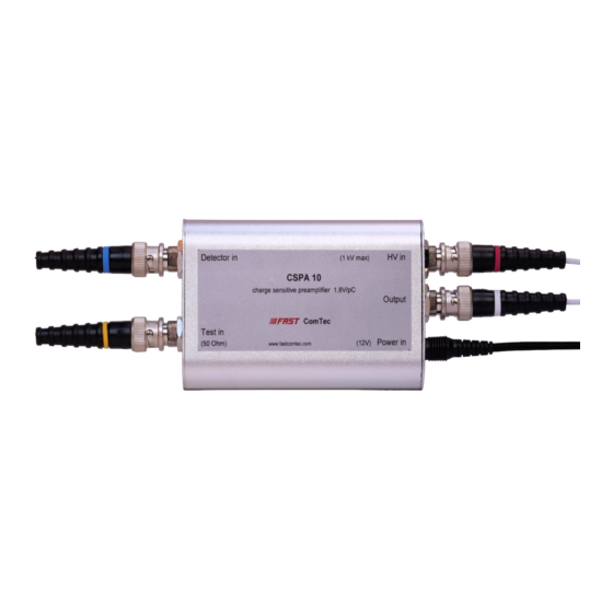
Page 11: Connector Types And Cables
Specifications 2.4 Connector types and cables Power: power connector 2.1 x 5.5 mm, DC connector, center positive; HV Input: SHV (BNC for CSPA1X-1B) Detector Input: SHV for the models CSPA1x-2S, CSPA1x-4S BNC for the models CSPA1x-1B Output: Test input: 2.5 Power Power supply voltage (Vs): + 12 volts nominal ( ext. -
Page 12: Controls And Connectors
3.1 General This section describes the functions of the controls and connectors located on the front and rear panels of the Model CSPA10...13. It is recommended that this section be read before proceeding with the operation of the preamplifier. 3.2 Front Panel / Rear Panel... -
Page 13: Installation
Any capacitance added to the input of the preamplifier will increase the noise contribution and degrade the rise time performance of the Model CSPA10…13. The capacitance should be minimized by using the shortest possible interconnecting cable between the detector and the preamplifier. -
Page 14: Operating Instructions
5 Operating Instructions 5.1 General The purpose of this section is to familiarize the user with the Model CSPA10...13 Preamplifier and to check that the unit is operating correctly. Since it is difficult to determine the exact system configuration in which the unit will be used, explicit operating instructions cannot be given. -
Page 15: Protection Circuit
Operating Instructions 5.5 Protection Circuit CSPA1x is designed among others to realize better usability and trouble-free power supply. The detector input is protected by implemented diodes network circuit. It minimally increases the internal capacitance and thus also the values of internal noise. You can disable this function as needed ( Fig. 7.1 Jumper J2: to pos. - Page 16 Operating Instructions : pulser and biased detector connected : puser without detector connected If R is not less than 2.0 keV for two microseconds unipolar Gaussian shaping time constant, the problem is in the electronics and probably in the preamplifier. If R is acceptable, but R is greater than 2.0 keV plus 10 eV/pF detector and connection capacitance,...
-
Page 17: Theory Of Operation
Fig. 6.1 shows a simplified equivalent circuit diagram of the hybrid amplifier module used in the CSPA10...13, which is a two stage amplifier. The first stage is high gain, and the second stage is low gain with an emphasis on supplying sufficient output current to drive a terminated coaxial cable. Rf (100 MΩ) and Cf (1.4 pF) are the feedback resistor and capacitor respectively... -
Page 18: Fig. 6.1: Simplified Circuit Diagram
Theory of Operation Fig. 6.1: Simplified circuit diagram ComTec GmbH... -
Page 19: Jumper Setting & Opening Of The Case
Jumper setting & opening of the case 7 Jumper setting & opening of the case Fig. 7.1: CSPA1X board with jumpers * 1-2 shorted - protection network active, 2-3 protection passive * 1-2 shorted – inp. ser. resistor = 0 Ohm 2-3 inp. -
Page 20: Appendix
Appendix 8 Appendix 8.1 Detailed Schematic of the CSPA10…13 Fig. 8.1: Detailed circuit diagram of CSPA1X ComTec GmbH... -
Page 21: Personal Notes
Appendix 8.2 Personal Notes ComTec GmbH...
Need help?
Do you have a question about the CSPA10 and is the answer not in the manual?
Questions and answers