
Related Manuals for Panasonic SA-AK600GC


Summary of Contents for Panasonic SA-AK600GC
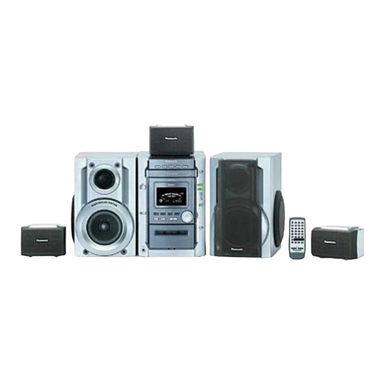
- Page 1 ORDER NO. MD0205110C3 CD Stereo System SA-AK600GC / SA-AK600GN Colour (S)... Silver Type TAPE SECTION : SG2 MECHANISM SERIES CD SECTION : RAE0152Z-3 TRAVERSE DECK SERIES SPECIFICATIONS Specifications...
- Page 2 AMPLIFIER SECTION Power output 10% THD, both channels driven 75 Hz Subwoofer 160 W (Total effective impedance: 4 1 kHz Front 35 W per ch (6 Center 70 W (8 Surround 40 W per ch (8 Total power in stereo mode (Front and Subwoofer) 230 W Total power in DOLBY DIGITAL mode 380 W...
- Page 3 DISC SECTION Sampling frequency 44.1 kHz Decoding 16 bit linear Beam source/wavelength Semiconductor laser/780 nm Number of channels Stereo Frequency response 20 Hz - 20 kHz (+1, -2 dB) Wow and flutter Below measurable limit Digital filter 8 fs D/A converter MASH (1 bit DAC) GENERAL Power supply...
- Page 4 Note that this unit will be seriously damaged if this setting is not made correctly. (There is no voltage selector for some countries, the correct voltage is already set.) 2. Before Repair and Adjustment Disconnect AC power, discharge Power Supply Capacitors C571-C574 and C581 through a 10 5W resistor to ground.
- Page 5 AC mains lead (For GN only) AM Loop antenna Power plug adaptor (for GC only) 5. Handling Precautions For Traverse Deck The laser diode in the traverse deck (optical pickup) may break down due to potential difference caused by static electricity of clothes or human body. So, be careful of electrostatic breakdown during repair of the traverse deck (optical pickup).
- Page 6 - Grounding for electrostatic breakdown prevention 1. Human body grounding Use the anti-static wrist strap to discharge the static electricity from your body. 2. Work table grounding Put a conductive material (sheet) or steel sheet on the area where the traverse deck (optical pickup) is placed, and ground the sheet. Caution : The static electricity of your clothes will not be grounded through the wrist strap.
- Page 7 6. Precaution of Laser Diode Caution : This product utilizes a laser diode with the unit turned "ON", invisible laser radiation is emitted from the pick up lens. / Wavelength : 780 nm / Maximum output radiation power from pick up : 100 W/VDE / Laser radiation from pick up unit is safety level, but be sure the followings:...
- Page 8 Wellenlänge : 780nm / Maximale Strahlungsleistung der Lasereinheit :100 W/VDE / Die Strahlung an der Lasereinheit ist ungefährlich, wenn folgende Punkte beachtet werden: 1. Die Lasereinheit nicht zerlegen, da die Strahlung an der freigelegten Laserdiode gefährlich ist. 2. Den werkseitig justierten Einstellregler der Lasereinhit nicht verstellen.
- Page 9 7. Operation Procedures...
- Page 11 8. Disassembly and Main Component Replacement Procedures “ATTENTION SERVICER” Some chassis components may have sharp edges. Be careful when disassembling and servicing.
-
Page 12: Table Of Contents
1. This section describes procedures for checking the operation of the major printed circuit boards and replacing the main components. 2. For reassembly after operation checks or replacement, reverse the respective procedures. Special reassembly procedures are described only when required. 3. - Page 13 Step 2 Remove the Top Cabinet. Step 3 Push the lever in the direction of the arrow.
- Page 14 Step 4 Pull out the CD tray as shown and remove the CD lid. Push back the CD tray after the CD lid has been removed.
- Page 15 Step 5 Release the 2 cathches, disconnect CN309 and CN310 and remove the CD changer base together with the CD changer. Step 6 Remove 15 screws. - Checking for Main, Panel , Sub-Transformer and Deck P.C.B...
-
Page 16: Checking Of Power P.c.b
- Checking for Power P.C.B. -
Page 17: Main Component Replacement Procedures
8.2. Main Component Replacement Procedures 8.2.1. Replacement of the Traverse Deck Step 1 Follow the procedures in ‘Disassembly of the Traverse Unit’ ( Step 1 - Step 4 ). Step 3 Desolder the 4 legs of the 2 motors and pull out the Servo P.C.B. Step 4 Widen the 3 bosses with a flat screwdriver and pull out the 3 pins. - Page 18 Step 5 Remove the flexible cable CN701. - Removal of the flexible cable. Push the top of the connector in the direction of the arrow 1, and then pull out the flexible cable in the direction of the arrow 2. Note: Insert a short pin into the flexible cable for traverse unit.
-
Page 19: Replacement Of The Power Amplifier Ic
Before installing the CD servo P.C.B., move the optical pickup towards the outer edge from the marking (black triangle). [Otherwise, the reset detect switch (S701) mounted on the CD servo P.C.B. may be damaged.] 8.2.2. Replacement of the Power Amplifier IC Step 1 Follow the procedures in ‘Checking Procedure for each major P.C.B.’... -
Page 20: Disassembly And Assembly Of The Traverse Unit
Step 3 Remove the 2 screws fixed to the Power Amplifier IC. Step 4 Unsolder the terminals of Power Amp IC and replace the respective component. 8.3. Disassembly and assembly of the Traverse Unit Step 1 Push the lever from position A to B. Step 2 Pull the stopper (black) in the direction of arrow 1 and push the lever in the direction of arrow 2. - Page 21 Step 4 Lift up the traverse unit and slide out the unit as shown. - Replacement of Traverse Unit Step 1 Place the traverse unit as shown. Step 2 Press in the lever shaft in the direction of arrow 1 as shown and push the traverse unit into the position in the direction of arrow 2.
-
Page 22: Disassembly And Assembly Of The Disc Tray
Step 4 Pull out the tray half way and push it back fully. Step 5 Push the lever to the initial position indicated ‘|---|’. 8.4. Disassembly and assembly of the Disc Tray Step 2 With lifting the claw in the direction of arrow 1, draw the clamp SW P.C.B. in the direction of arrow 2. - Page 23 Step 4 Insert the gear with hexagonal wrench into the hole. Step 5 Rotate the hexagonal wrench in the direction of arrow (clockwise), and then open the disc tray fully. Step 6 Upset the CD changer unit again. Step 7 Release both the claws, and then draw the disc tray.
- Page 24 Step 8 With forcing the left guide bar manually because the left guide bar interferes with claw, draw the disc tray. - Installation of the disc tray after replacement Step 1 Slide the drive rack fully in the direction of the arrow.
- Page 25 Step 2 Holding the drive rack, not to move, install the disc tray. Step 3 Align the drive rack with the drive gear.
- Page 26 Step 4 Holding the disc tray manually, rotate the pulley gear in the direction of arrow. Step 5 Rotate the gear 5 or 6 times manually, and then push the disc tray. 9. Self-Diagnostic Function 9.1. Self-diagnostic display This unit is equipped with a self-diagnostic display function which, if a problem occurs, will display an error code corresponding to the problem.
- Page 27 9.3. Cassette Mechanism Test (For error code H01, H02, H03, F01, F02) 1. Press “TAPE, DECK 1/2” to select Deck 2. 2. Load a cassette tape with the erasure prevention tab, remove from left side only and close the cassette holder. 3.
- Page 28 4. Load a cassette tape with the erasure prevention tab, remove from right side only and close the cassette holder. 5. Press “REVERSE FM MODE/BP” (Tape will be stop after 2 seconds) 6. Load a pre-recorded tape with both side record tabs intact and close the cassette holder.
- Page 29 9.6. How to get out from Self-Diagnostic function 1. Press “Power” button OFF. 9.7. Power Amplifier Failure (F61) 1. When power amplifier fail, F61 will indicate automatically. 10. Description of Error Code 10.1. Error detection for Cassette Mechanism block Error Error Problem condition Display...
- Page 30 Error Error Problem condition Display REST SW detection error CD does not function. This error occurs when the Optical Pick Up REST (S701) is not detected within the specified time (about 8 seconds) CD tray opens automatically CLAMP switch (S4) NG (Check & Replace) Does not startup when BOTTOM switch (S5) NG (Check &...
- Page 31 11.2. CD Automatically Adjustment result indication Under CD test mode, pressing the numeric key ‘0’ on the remote controller will display the auto adjustment result. FLOCK, TLOCK and CLVS status shall be shown as below: During the above display, executing CD PLAY will display auto adjustment result for CD PLAY mode.
- Page 32 12. Measurements and Adjustments 12.1. Cassette Deck Section - Measurement Condition - Make sure head, capstan and press roller are clean. - Judgeable room temperature 20 ± 5 °C (68 ± 9°F) - Measuring instrument - EVM (Electronic Volmeter) - Digital quency counter - Test Tape - Tape speed gain adjustment (3 kHz, -10 dB);...
- Page 33 12.1.3. Bias Frequency check 1. Set the unit to “AUX” position. 2. Insert the Normal blank tape (QZZCRA) into DECK and set the unit to “REC” mode ( use “REC” key). 3. Check so that the output frequency is within the standard value. Standard Value: 86 ±8 kHz 12.2.
- Page 34 Tuner section Fig. 9 FIg. 10...
- Page 35 13. Illustration of IC’s, Transistors and Diodes 14. Terminal Function of IC’s 14.1. IC701 (AN8885SBE1) Servo Amplifier Pin No. Mark Function Tracking signal input 1 Tracking signal input 2 Power supply Focus signal input terminal 1 Focus signal input terminal 2 APC amp input APC amp output RFsumming output...
- Page 36 Pin No. Mark Function FE amp input VREF Reference voltage output TBAL Tracking balance control FBAL Focus balance control 14.2. IC702 (MN662790RSC) Servo processor/ Digital signal processor/ Digital filter/ D/A converter Pin No. Mark Function BCLK N.C. LRCK N.C. SRDATA O N.C.
- Page 37 Pin No. Mark Function SQCK External clock signal input for sub-code Q resistor SUBQ Sub-code Q code output DMUTE Muting input (“H” : mute) STAT Status signal output (CRC,CUE,CLVS, TTSTVP,FCLV,SQCK) /RST Reset signal input SMCK 1/2-diveded clock signal of crystal osscillating at MSEL = “H”...
- Page 38 Pin No. Mark Function Focus error signal input (analog input) Tracking error signal input (analog input) RFENV RF envelope signal input VDET Vibration detection signal input ("H" : detection) Off-track signal input ("H" : off track) TRCRS Track cross signal input /RFDET RF detection signal...
- Page 39 Pin No. Mark Function VCOF2 VCO Loop filter for 33.8688 MHz conversation terminal for 16.9344 MHz crystal mode, must use other circuit SUBC Sub-code serial data output SBCK Clock input for sub- code serial data X1 IN Crystal oscillating circuit input (f = 16.9344MHz) X2 OUT Crystal oscillating...
- Page 40 Pin No. Mark Function IOSEL Mode Switching Terminal /TEST Test input AVDD1 Power supply input (for analog circuit) OUTL Left channel audio signal output AVSS1 OUTR Right channel audio signal output RSEL RF signal polarity assignment input (at "H" level, RSEL="H", at "L"...
- Page 41 Pin No. Mark Function /RST RESET output terminal N.C. Motor Drive (2) input Turntable motor drive signal (“L :ON) N.C. Motor driver (1) input N.C. PVCC1 I Power supply (1) for driver PGND1 - Ground connection (1) for driver N.C. Motor driver (1) reverse- action output Motor driver (1) forward-...
- Page 42 Pin No. Mark Function SD_IN Tuner signal detect input MK_IN2 Mech condition input MK_IN1 mech condition input KEY2 Key 2 input KEY1 Key 1 input LM_SL Level meter left LM_SR Level meter right CHG_AD2 I Changer SW A-D detection input 2 CHG_AD1 I Changer SW A-D detection input 1...
- Page 43 Pin No. Mark Function SYNC AC Failure Detect Input CHG_CCW O Changer motor counter clockwise output CHG_CW O Changer motor clockwise output CHG_HLF O Changer half drive output CHG_PGR O Changer plunger output CHG_SW2 I CD changer switch 2 input CHG_SW1 I CD changer switch 1 input...
- Page 44 Pin No. Mark Function SER2 DDD_DAT/VOL_DAT/ ASP_CLK SER1 VOL_CLK/MK_CLK AVSS Analog ground (0V) Vref Reference for A-D SER7 4ch volume latch DSP_ DDD_MIACK MIACK 15. Block Diagram 16. Schematic Diagram (All schematic diagrams may be modified at any time with the development of the new technology) Note: S501...
- Page 45 S901 : CD switch S902 : Tape switch S903 : Tuner Band switch S904 : AUX switch S905 : -V/ REW switch S906 : +V/ FF switch S907 : Stop/ Demo switch S908 : CD 1 switch S909 : CD 2 switch S910 : CD 3 switch S911...
- Page 46 S954 : Recinh_f switch - The voltage value and waveforms are the reference voltage of this unit measured by DC electronic voltmeter (high impedance) and oscilloscope on the basis of chassis. Accordingly, there may arise some error in voltage values and waveformsdepending upon the internal impedance of the tester or the measuring unit.
- Page 47 20. Parts Location and Replacement Parts List Notes:...
- Page 48 - Important safety notice: Components identified by mark have special characteristics important for safety. Furthermore, special parts which have purposes of fire-retardent (resistors), high-quality sound (capacitors), low noise (resistors), etc are used. When replacing any of these components, be sure to use only manufacturer’s specified parts shown in the parts list.
- Page 49 Ar : Arabic Du : Dutch It : Italian Sp : Spanish Cf : Canadian French En : English Ko : Korean Sw : Swedish Cz : Czech Fr : French Po : Polish Co : Traditional Chinese Da : Danish Ge : German...
- Page 50 20.1.2. Deck Mechanism Parts List...
- Page 51 Ref. No. Part No. Part Name & Description Remarks CASSETTE DECK RED0067 R/P HEAD BLOCK UNIT RDG0300 REEL BASE GEAR RDG0301 WINDING RELAY GEAR RDK0026 MAIN GEAR RDV0033-4 WINDING BELT RDV0064 CAPSTAN BELT RMB0312 TRIGGER LEVER SPRING RMB0400 REEL SPRING RMB0403 HEAB PANEL SPRING RMB0404...
- Page 53 20.2.2. CD Loading Mechanism Parts List...
- Page 54 Ref. No. Part No. Part Name & Description Remarks TRAVERSE DECK RML0517 TIMING LEVER RML0516 PLUNGER LEVER RMB0551 UPPER SPINDLE SPRING RMQ0744 LOWER HOOK RDV0056 BELT RML0525 FRONT LOCK LEVER RML0526 DISC LEVER RDG0424 DRIVE GEAR RDG0425 CHANGE GEAR RDG0427 TRAVERSE CAM GEAR RDG0428 TRAVERSE RELAY GEAR...
- Page 55 Ref. No. Part No. Part Name & Description Remarks RDG0431 RELAY GEAR ‘B’ RME0262 DISK LEVER SP. RMA1105 SUPPORT PLATE RAE0152Z-3 TRAVERSE 358-1 SHGD113-1 FLOATING CUSHION 358-2 SNSD38 TRV MOTOR ASSY SCREW 358-3 RAF0150A-4S 50A OPTICAL PICKUP 358-4 RDG0247 DRIVE GEAR 358-5 RDG0248 RELAY GEAR...
- Page 58 20.3.2. Cabinet Parts List...
- Page 59 Ref. No. Part No. Part Name & Description Remarks CABINET AND CHASSIS REEX0083 14P FFC WIRE REEX0156 30P FFC WIRE REEX0170 19P FFC WIRE REM0072-3 RGK1342B-Q TOP ORNAMENT RGK1344A-Q PANEL ORNAMENT RGK1345A-Q CASS. ORNAMENT RGKX0106-H CD LID ORNAMENT RGKX0107-S CD LID RGKX0108 FL FILTER RGL0538-W...
- Page 60 20.4. Electrical Parts List Ref. No. Part No. Part Name & Description Remarks PRINTED CIRCUIT BOARD REPX0192D CD SERVO P.C.B. [M](RTL) REPX0286B MAIN/ TUNER P.C.B. [M](RTL) REPX0285B PANEL P.C.B. [M]GC(RTL) REPX0285C PANEL P.C.B. [M]GN(RTL) REPX0285B TACT SWITCH (1) P.C.B. [M]GC(RTL) REPX0258C TACT SWITCH (1) P.C.B.
- Page 61 Ref. No. Part No. Part Name & Description Remarks IC809 C0ABBB000067 IC DUAL OP AMP IC810 C0ABBB000067 IC DUAL OP AMP IC811 C0JBAS000056 IC DUAL BILATERAL SWITCH IC951 CNB13030R2AU IC PHOTO INTERUPTOR IC1000 C1AA00000612 IC ANALOG SW IC1001 AN7326K IC REC/PB TRANSISTORS B1GACFGG0004 TRANSISTOR...
- Page 62 Q571 KRC102MTA TRANSISTOR...
- Page 63 Ref. No. Part No. Part Name & Description Remarks Q572 B1AAGC000007 TRANSISTOR Q573 2SB621ARSTA TRANSISTOR Q601 2SB621ARSTA TRANSISTOR Q602 KTC3875GRTA TRANSISTOR Q603 KTC3875GRTA TRANSISTOR Q604 KRC102STA TRANSISTOR Q605 B1ADCF000001 TRANSISTOR Q606 KRC103STA TRANSISTOR Q607 B1ADCF000001 TRANSISTOR Q701 B1ADCF000001 TRANSISTOR Q802 KRC102STA TRANSISTOR Q803...
- Page 64 D304 B0ADCJ000020 DIODE...
- Page 65 Ref. No. Part No. Part Name & Description Remarks D305 B0BC5R000009 DIODE D306 B0BC7R500001 DIODE D307 MA2J72800L DIODE D308 RL1N4003S-P DIODE D309 B0BC5R000009 DIODE D311 B0BC5R600003 DIODE D312 RL1N4003S-P DIODE D313 MA2J72800L DIODE D314 MA2J72800L DIODE D315 MA2J72800L DIODE D316 MA2J72800L DIODE D317...
- Page 66 D578 1T3T DIODE [M]GN...
- Page 67 Ref. No. Part No. Part Name & Description Remarks D580 B0BA6R600008 DIODE [M]GN D580 B0BA7R000005 DIODE [M]GC D581 1T3T DIODE [M]GC D582 1T3T DIODE [M]GC D596 B0AACK000004 DIODE D600 1SS355TE17 DIODE [M]GC D601 1SS355TE17 DIODE [M]GN D602 1SS355TE17 DIODE [M]GC D605 1SS355TE17 DIODE...
- Page 68 S701 RSH1A043-U SW RESET...
- Page 69 Ref. No. Part No. Part Name & Description Remarks S901 EVQ21405R SW CD S902 EVQ21405R SW TAPE S903 EVQ21405R SW TUNER BAND S904 EVQ21405R SW AUX S905 EVQ21405R SW -V/ REW S906 EVQ21405R SW +V/ FF S907 EVQ21405R SW STOP/DEMO S908 EVQ21405R SW CD 1...
- Page 70 Ref. No. Part No. Part Name & Description Remarks CS951 RJU071H09M1 CONNECTOR COILS & TRANSFORMERS L300 RLBV252AV-Y LINE COIL L301 RLBV252AV-Y LINE COIL L500 RLQZ371 LINE FILTER L602 G0C101JA0030 INDUCTOR L603 G0C3R3JA0030 COIL L800 RLBN102V-Y CHIP INDUCTOR L801 RLQZB470KT-D RF CHOKE COIL L802 RLQZ150M-0 BEADS CHOKE...
- Page 71 [M]GC...
- Page 72 Ref. No. Part No. Part Name & Description Remarks FUSE HOLDERS FC501 EYF52BC FUSE HOLDER FC502 EYF52BC FUSE HOLDER FC503 EYF52BC FUSE HOLDER [M]GC FC504 EYF52BC FUSE HOLDER [M]GC FUSE PROTECTOR FP583 K5G402AA0002 FUSE PROTECTOR FP584 K5G102AA0002 FUSE PROTECTOR HOLDERS H502 K1YF12000004 WIRE HOLDER...
- Page 73 Ref. No. Part No. Part Name & Description Remarks W602 REXX0313 7P FLAT WIRE W603 RWJ1104215XX WIRE W605 RWJ1106100XX BABY P.T. TO MAIN FL W1304 RWJ1109085XX 9P FLAT WIRE W1903 RWJ0102050CK MAIN-MECHA MOTOR WIR JUMPER PLATE RJR0199 JUMPER PLATE [M]GC RESISTORS ERDS2TJ102T 1K 1/4W...
- Page 74 Ref. No. Part No. Part Name & Description Remarks R243 ERJ3GEYJ823V 82K 1/16W R244 ERJ3GEY0R00V 0 1/16W R245 ERJ3GEYJ153V 15K 1/16W R246 ERJ3GEYJ153V 15K 1/16W R247 D0GB334JA002 330K 1/16W R248 ERJ3GEYJ222V 2.2K 1/16W R249 D0GB152JA002 1.5K 1/16W R250 D0GB332JA002 3.3K 1/16W R251 ERJ3GEYJ104V 100K 1/16W...
- Page 75 Ref. No. Part No. Part Name & Description Remarks R327 D0GB562JA002 5.6K 1/16W R328 ERJ3GEYJ472V 4.7K 1/16W R329 ERJ3GEYJ103V 10K 1/16W R330 ERJ3GEYJ103V 10K 1/16W R331 ERJ3GEYJ103V 10K 1/16W R332 ERJ3GEYJ103V 10K 1/16W R333 ERJ3GEYJ103V 10K 1/16W R334 ERJ3GEYJ103V 10K 1/16W R335 ERJ3GEYJ103V 10K 1/16W...
- Page 76 Ref. No. Part No. Part Name & Description Remarks R381 ERJ3GEYJ104V 100K 1/16W R382 ERJ3GEY0R00V 0 1/16W R383 RLBN102V-Y INDUCTOR R384 ERJ3GEYJ103V 10K 1/16W R386 ERJ3GEY0R00V 0 1/16W R387 ERJ3GEY0R00V 0 1/16W R388 ERJ3GEYJ102V 1K 1/16W R389 ERJ3GEYJ103V 10K 1/16W R390 ERJ3GEY0R00V 0 1/16W...
- Page 77 Ref. No. Part No. Part Name & Description Remarks R439 D0GB333JA002 33K 1/16W R440 ERJ3GEYJ222V 2.2K 1/16W R441 D0GB334JA002 330K 1/16W R442 D0GB680JA019 68 1/16W R443 ERJ3GEYJ823V 82K 1/16W R444 ERJ3GEY0R00V 0 1/16W R445 ERJ3GEYJ153V 15K 1/16W R446 ERJ3GEYJ153V 15K 1/16W R447 D0GB334JA002 330K 1/16W...
- Page 78 Ref. No. Part No. Part Name & Description Remarks R524 ERDS2TJ124T 120K 1/4W R525 ERDS2TJ154T 150K 1/4W R526 ERDS2TJ124T 120K 1/4W R527 ERDS2TJ124T 120K 1/4W R528 ERDS2TJ154T 150K 1/4W R529 ERDS2TJ223T 22K 1/4W R532 ERDS2TJ103T 10K 1/16W R537 ERDS1FVJ100T 10 1/2W R538 ERDS1FVJ100T 10 1/2W...
- Page 79 Ref. No. Part No. Part Name & Description Remarks R615 ERJ3GEYJ102V 1K 1/16W R616 ERJ3GEYJ102V 1K 1/16W R617 D0GB271JA002 270 1/16W R618 D0GB271JA002 270 1/16W R619 D0GB151JA008 150 1/16W R620 D0GB121JA002 120 1/16W R621 D0GB152JA002 1.5K 1/16W R622 ERJ3GEYJ223V 22K 1/16W R623 ERJ3GEYJ223V 22K 1/16W...
- Page 80 Ref. No. Part No. Part Name & Description Remarks R669 ERJ3GEYJ472V 4.7K 1/16W R670 ERJ3GEYJ472V 4.7K 1/16W R671 ERJ3GEYJ472V 4.7K 1/16W R672 ERJ3GEYJ102V 1K 1/16W R673 ERJ3GEYJ104V 100K 1/16W R674 ERJ3GEYJ223V 22K 1/16W R675 D0GB151JA008 150 1/16W R676 ERJ3GEYJ102V 1K 1/16W R677 ERJ3GEYJ473V 47K 1/16W...
- Page 81 Ref. No. Part No. Part Name & Description Remarks R742 ERJ6GEYJ224V 220K 1/10W R744 D0GB124JA002 120K 1/16W R749 ERJ3GEYJ472V 4.7K 1/16W R750 ERJ6GEYJ4R7V 4.7 1/10W R753 D0GB100JA002 10 1/16W R801 ERJ3GEYJ472V 4.7K 1/16W R802 D0GB183JA002 18K 1/16W R803 D0GB105JA002 1M 1/16W R804 ERJ3GEYJ104V 100K 1/16W...
- Page 82 Ref. No. Part No. Part Name & Description Remarks R851 ERJ3GEYJ223V 22K 1/16W R852 ERJ3GEY0R00V 0 1/16W R853 ERJ3GEY0R00V 0 1/16W R854 ERJ3GEYJ221V 220 1/16W R855 ERJ3GEYJ123V 12K 1/16W R856 ERJ3GEYJ123V 12K 1/16W R857 ERJ3GEYJ221V 220 1/16W R858 ERJ3GEYJ221V 220 1/16W R859 ERJ3GEYJ221V 220 1/16W...
- Page 83 Ref. No. Part No. Part Name & Description Remarks R1203 D0GB183JA002 18K 1/16W R1204 ERJ3GEYJ103V 10K 1/16W R1205 ERJ3GEYJ222V 2.2K 1/16W R1206 ERJ3GEYJ104V 100K 1/16W R1207 ERJ3GEYJ102V 1K 1/16W R1209 ERJ3GEYJ102V 1K 1/16W R1210 D0GB333JA002 33K 1/16W R1302 D0GB101JA002 100 1/16W R1303 D0GB475JA008 4.7M 1/16W...
- Page 84 R3206 ERJ3GEYJ471V 470 1/16W...
- Page 85 Ref. No. Part No. Part Name & Description Remarks R3207 ERJ3GEYJ471V 470 1/16W R3208 ERJ3GEYJ472V 4.7K 1/16W R3209 ERJ3GEYJ472V 4.7K 1/16W R3210 ERJ3GEYJ221V 220 1/16W R3211 ERJ3GEYJ104V 100K 1/16W R3212 ERJ3GEYJ221V 220 1/16W R3213 ERJ3GEYJ104V 100K 1/16W R3214 ERJ3GEYJ221V 220 1/16W R3215 ERJ3GEYJ104V 100K 1/16W...
- Page 86 Ref. No. Part No. Part Name & Description Remarks R3405 ERJ3GEYJ103V 10K 1/16W R3406 ERJ3GEYJ471V 470 1/16W R3407 ERJ3GEYJ471V 470 1/16W R3408 ERJ3GEYJ472V 4.7K 1/16W R3409 ERJ3GEYJ472V 4.7K 1/16W R3410 ERJ3GEYJ221V 220 1/16W R3411 ERJ3GEYJ104V 100K 1/16W R3412 ERJ3GEYJ221V 220 1/16W R3413 ERJ3GEYJ104V 100K 1/16W...
- Page 87 Ref. No. Part No. Part Name & Description Remarks C234 ECEA1HKA010B 1 50V C235 ECEA1HKA010B 1 50V C236 ECJ1VC1H101K 100P 50V C237 ECUV1H101JCV 100P 50V C238 ECEA1HKA3R3B 3.3 50V C239 ECEA1HKA010B 1 50V C240 ECEA1HKAR22B 0.22 50V C241 ECEA1HKA010B 1 50V C242 ECEA1HKA0R1B 0.1 50V...
- Page 88 Ref. No. Part No. Part Name & Description Remarks C363 ECUV1C104KBV 0.1 16V C364 ECEA1CM221B 220 16V C365 ECJ1VB1E103K 0.01 25V C366 ECJ1VB1E103K 0.01 25V C367 ECJ1VC1H101K 100P 50V C368 ECEA1CKA100B 10 16V C369 RCE1HKN100BG 10P 50V C370 ECEA1CKA100B 10 16V C371 F1H1A2240004 0.22 10V...
- Page 89 Ref. No. Part No. Part Name & Description Remarks C441 ECEA1HKA010B 1 50V C442 ECEA1HKA0R1B 0.1 50V C449 F1H1C393A089 0.039 16V C490 ECJ1VB1H682K 6800P 50V C501 ECBT1H821KB5 820P 50V C502 ECBT1H821KB5 820P 50V C503 ECBT1H821KB5 820P 50V C504 ECBT1H821KB5 820P 50V C505 ECBT1H821KB5 820P 50V...
- Page 90 Ref. No. Part No. Part Name & Description Remarks C576 ECA1HM101B 100 50V C577 ECA1EM331B 330 25V C577 ECKR1H103ZF5 0.01 50V C578 ECA1JM101B 100P 63V C578 ECKR1H103MD5 0.01 50V C579 ECA1HM470B 47 50V C579 ECKR1H103MD5 0.01 50V C580 ECA1HM470B 47 50V C580 ECA2AM100B 10 100V...
- Page 91 Ref. No. Part No. Part Name & Description Remarks C641 ECUV1H561KBV 560P 50V C642 ECUV1H561KBV 560P 50V C643 ECJ1VB1H103K 0.01 50V C644 ECJ1VC1H101K 100P 50V C645 ECUV1C104ZFV 0.1 16V C646 ECJ1VC1H101K 100P 50V C647 ECJ1VC1H101K 100P 50V C648 ECUV1H561KBV 560 50V C701 ECEA0JKA330I 33 6.3V...
- Page 92 Ref. No. Part No. Part Name & Description Remarks C803 ECUV1C104KBV 0.1 16V C804 ECEA1CKA101B 100 16V C805 F1H1H103A753 0.01 50V C806 ECUV1C104ZFV 0.1 16V C807 ECUV1C104ZFV 0.1 16V C808 VCEA1CJH221B 220P 16V C809 ECUV1C104ZFV 0.1 16V C810 VCEA1CJH221B 220P 16V C811 ECJ1VB1H103K 0.01 50V...
- Page 93 Ref. No. Part No. Part Name & Description Remarks C863 ECJ1VC1H101K 100P 50V C864 ECJ1VC1H470K 47P 50V C874 ECJ1VC1H470K 47P 50V C875 ECJ1VC1H470K 47P 50V C876 ECUV1C104ZFV 0.1 16V C901 ECJ1VC1H101K 100P 50V C902 ECJ1VC1H101K 100P 50V C903 F1H1H103A753 0.01 50V C904 ECEA0JKA470B 47 6.3V...
- Page 94 Ref. No. Part No. Part Name & Description Remarks C1319 ECA1CAK101XB 100 16V C1320 ECA1HAK010XB 1 50V C1321 F0A2A472A015 4700P 100V C1322 ECQP2A102JZT 1000P 100V C1323 ECEA1HKN010B 1 50V C1324 ECA1CAK470XB 47 16V C1325 ECJ1VB1E103K 0.01 25V C1326 ECA1CAK100XB 10 16V C1371 ECJ1VB1H103K 0.01 50V...
- Page 95 Ref. No. Part No. Part Name & Description Remarks C3403 ECUV1C104KBV 0.1 16V C3404 ECEA1CKA100B 10 16V C3405 ECJ1VB1H222K 2200P 50V C3406 ECEA1CKA100B 10 16V C3407 ECJ1VB1H222K 2200P 50V C3408 ECEA1CKA100B 10 16V C3409 ECJ1VB1H222K 2200P 50V C3410 ECEA1HKA010B 1 50V C3411 ECJ1VC1H101K 100P 50V...
- Page 96 20.5. Packing Materials & Accessories Parts List Ref. No. Part No. Part Name & Description Remarks PACKING MATERIALS RPGX0872 PACKING CASE [M]GN RPGX0873 PACKING CASE [M]GC RPN1406-1 POLYFOAM RPFX0007 MIRAMAT BAG ACCESSORIES N2QAGB000018 REMOTE CONTROLLER A1-1 251200F1F R/C BATTERY COVER RJA0019-2X AC CORD [M]GC...
- Page 97 Printed in Singapore / P020500001 D/K/J/N/L/PRT...
- Page 98 C1BB00000574 RSN311W64B-P C0GAM0000005 TC74HCU04AF M62444FPE1 C1BB00000654 (42P) AN8885SBE1 C0FBZK000005 (44P) C0ABBB000067 C2BBGF000348 (100P) C2HBZH000001 (100P) MN662790RSC (80P) CNB13030R2AU C0AABB000117 AN8739SBTE2 AN7326K C5AB00000105 C1AA00000612 BR93LC46FE2 (8P) B1GACFGG0004 KRA102MTA UPC29M33HF C0JBAS000056 KTC3199GRTA B1AAKD000009 KRC102MTA B1AAAL000002 KTA12710YTA B1AAGC000007 KTA1504GRTA KTC3205YTA 2SD09650RA 2SB621ARSTA 2SD0592ARA KRA102STA KRC111STA B0ADCJ000020...
- Page 99 IC701 AN8885SBE1 OPTICAL PICKUP SERVO AMP SEMICONDUCTOR LASER OFTR OFTR OFTR RFEQ1 Q701 3TENV LASER RFEQ2 POWER DRIVE NRFDET /RFDET /RFDET FEOUT SUBTRACTOR VREF PHOTO DETECTOR TEOUT SUBTRACTOR VREF BAND VREF TRACKING FOCUS COIL COIL DIGITAL AUDIO SYNDROME INTERFACE CALCULATION PHASE FREQUENCY COMPARATOR...
- Page 100 IC804 Q805 M62444FPE1 SWITCHING 4CH ELECTRIC VOLUME (32) (31) (30) (29) (28) (27) (26) INT2 IC805 C0ABBB000067 DUAL OP AMP D406 Q404 (D206) Q803 Q813 Q310 (Q204) D805,D806 IC806 CURRENT SWITCHING SWITCHING SWITCHING AMPLIFIER UPC29M33HF VOLTAGE Q810 STABILISER STABILISER Q811 Q812 Q814 CURRENT...
- Page 101 SLOUT(R) SWCH SL(R) 27(28) 23(24) SMUTE SUBQ LRCKA PORT3 IC802 LRCKDA LRCK C0FBZK000005 IC803 AUDIO DECODER DSP_MICK BCKA /MICK C2HBZH000001 25(26) LOUT2(R) DIGITAL SOUND BCKDA BICK PROCESSOR MIACK MIACK 16~18,22 SD0~2, SDTI1~3,SDTO SDI0 LOCK LOCK MCLK 29(31) 30(32) SER2 MIDIO XOUT MILP X801...
- Page 102 FILTER R/P HEAD Q1101 (L ch) Q1302 (Q1201) HIGH DECK CURRENT MUTING GAIN CONTROL IC1001 AN7326K FILTER P/B REC AMP 22(1) 21(2) 20(3) 19(4) 16(7) RIPPLE REJECTION LOGIC REC AMP (L) MUTE SWITCHING Q1304 Q1303 IC1000 REC_H INVERTER INVERTER C1AA00000612 ANALOG SWITCH (FOR RECORDING) IC303...
- Page 103 FROM IC600 17(26) 18(25) TUNER IC302 PACK C0AABB000117 Q402(Q202) Q407(Q207) D402(D202) HEADPHONE (24) MUTING VOL OUT1(2) CONTROL 4(39) SWITCH IN1B(2B) Q307 5(38) Q403, IN1C(2C) AUDIO Q203 MUTING MUTING SWITCH CONTROL LT(RT) 41(42) IC300 SWITCH REC_B1/SUR2 (REC_B2/SUR1) C1BB00000654 AUDIO SOUND PROCESSOR AUX2 6(37) IN1D(2D)
- Page 104 IC501 RSN311W64B-P POWER CONTROL CIRCUIT POWER CONTROL/PROTECTION CIRCUIT (25) (19) (11) D502 D501 JK503 SUBWOOFER FILTER SPEAKER FILTER JK503 Q505 Q506 SPEAKER SWITCH SWITCH FILTER JK503 SURROUND SPEAKER FILTER JK501 (JK502) Q501,Q502 FRONT SPEAKER SWITCHING Q976 Q571 IC500 SYNCHRONISING STABILISER SWITCH C5BA00000105 D626...
- Page 105 CD LOADING P.C.B (REP2578A-N) 1 2 3 4 5 6 7 8 9 10 2 3 4 CD DETECT P.C.B SPINDLE POSITION P.C.B (REP2578A-N) (REP2578A-N) 1 2 3 4...
- Page 106 DECK P.C.B. (REPX0304A) R1377 C1101 L1301 C1323 J1021 C1321 J1061 C1103 R1101 C1201 J1019 R1201 C1322 C1203 C1121 C1104 J1017 C1325 R1302 C1303 C1204 C1318 R1102 Q1313 C1122 C1106 R1333 C1108 C1302 C1223 IC1000 J1022 R1330 C1123 C1109 C1319 C1301 R1303 R1334 R1336...
- Page 107 HEADPHONE P.C.B. (REPX0285B...GC) (REPX0285C...GN) PHONES H603B/W603 L904 JK901 L905 C907 SPEAKER TERMINAL P.C.B. (REPX0288B...GC) (REPX0288C...GN) SPEAKERS CNTR SURROUND SW_L- SW_L+ JK502 C535 C531 C533 C532 J599 C534 J590 R540 J592 R542 J589 J593 J598 E501 CP520/W521 C539 C537 C540...
- Page 108 MAIN / TUNER P.C.B. (REPX0286B) J280 J599 R831 J355 J281 Q809 R849 J283 R829 J204 R336 C3409 J284 J600 J207 J473 CN309 J422 C3406 C829 R3215 J287 C320 J217 C823 R320 J218 J290 C828 J363 CN310 J551 J292 J291 C321 C322 J293 J401...
- Page 109 D809 J599 J201 J203 JK801 J356 R860 J610 C838 R849 J277 C839 J486 D813 J412 R829 C857 R884 J600 J423 R838 R840 C823 C841 C829 L801 C802 R839 J215 C842 J433 C843 C822 C823 C801 J219 C844 J288 R855 J289 R841 C828 C845...
- Page 110 PANEL P.C.B. (REPX0285B...GC) (REPX0285C...GN) D612 S608 D611 R617 DIGITAL IN D614 D613 R618 FL600 J604 S605 D601 J927 D600 SSEQ J933 R635 J934 R605 R651 J612 S604 J656 R683 R643 C626 R644 R609 C627 PRSET_EQ R666 IC600 R645 R604 R693 D624 R637 D625...
- Page 111 S606 R606 R687 R685 R688 R684 J927 C619 1 2 3 4 R686 J608 J607 J933 H602A/W602 J609 C602 J934 R640 R641 J612 R636 J655 C609 J656 J613 L602 R653 R654 J614 R655 J911 J616 R611 R647 J679 C631 D616 J669 C643 R631...
- Page 112 POWER P.C.B. (REPX0284A) CP503 CP504 J549 J597 J518 J557 J572 J573 J578 J553 J565 R512 J598 R576 R574 R522 R521 J531 J533 J534 R532 C501 J520 J580 J515 C511 C506 J513 J562 R517 C512 R518 C573 C516 C509 R515 C515 R525 R519 J552...
- Page 113 CD SERVO P.C.B (REPX0192D) (RF) TP20 X701 TJ701 TP23 C717 R714 TP19 TP21 TP29 C716 C721 R709 C744 TP24 C722 R712 TP18 C723 C724 R742 C725 TP25 IC701 TP26 TP27 C731 C753 TP22 C754 C711 J702 C718 C712 IC702 C713 J712 R705 C747...
- Page 114 TACT SWITCH (1) TACT SWITCH (2) P.C.B. (REPX0285B...GC) P.C.B. (REPX0285B...GC) (REPX0258C...GN) (REPX0258C...GN) VOLUME VR900 J951 C901 J950 R914 R913 R912 R911 C905 C903 R910 C904...
- Page 115 AC TRANSFORMER P.C.B. (REPX0288B...GC) CAUTION RISK OF ELECTRIC SHOCK AC VOLTAGE LINE. PLEASE DO NOT TOUCH THIS P.C.B D574 C572 RL502 T501 (POWER TRANSFORMER) D572 J507 D582 R570 PRIMARY J506 D581 D570 J500 D957 D571 R581 C576 C570 SECONDARY R580 FP584 Q573 D575...
- Page 116 AC TRANSFORMER P.C.B. (REPX0288C...GN) CAUTION RISK OF ELECTRIC SHOCK AC VOLTAGE LINE. PLEASE DO NOT TOUCH THIS P.C.B C572 D574 RL502 T501 (POWER TRANSFORMER) D577 D572 D571 R570 PRIMARY J506 D570 J500 D957 R573 R581 C576 Q573 C570 R580 SECONDARY FP584 D575 FP583...
- Page 117 SCHEMATIC DIAGRAM -1 : +B SIGNAL LINE : CD-DA SIGNAL LINE OPTICAL PICKUP CIRCUIT CD SERVO CIRCUIT R701 LASER DIODE C701 <3.2V> 6.3V33 ((0V)) <2.7V> ((2.3V)) Q701 Q701 B1ADCF000001 C703 <0.9V> LASER POWER DRIVE 6.3V100 ((2V)) R750 LD GND NBOUT C704 C714 6.3V100...
- Page 118 SCHEMATIC DIAGRAM - 2 : +B SIGNAL LINE : CD SIGNAL LINE : CD-DA SIGNAL LINE CD SERVO CIRCUIT R717 C727 C725 50V1 R721 1000P C726 C731 1000P 6.3V220 C730 R718 C728 50V1 C754 C732 C733 470P 6.3V220 LCH OUT A.GND RCH OUT C753...
- Page 119 SCHEMATIC DIAGRAM - 3 : +B SIGNAL LINE DSP/MAIN CIRCUIT R848 R803 R806 R844 OUTPUT 4.7K 4.7K OPTICAL INPUT L801 JK801 RLQZB470KT-D C801 C802 C805 50V4.7 0.01 C853 IC808 1000P C0JBAS000056 DUAL BILATERAL SWITCH C803 R804 IC801 IC801 100K TC74HCU04AF CMOS INVERTER C851 IC808...
- Page 120 SCHEMATIC DIAGRAM - 4 : +B SIGNAL LINE : MAIN SIGNAL LINE DSP/MAIN CIRCUIT R3204 R3200 C3200 R3201 R3203 16V22 IC806 UPC29M33HF VOLTAGE STABILISER R3208 R3202 4.7K 100K IC806 IC810 IC810 C0ABBB000067 DUAL OP AMP L804 RLBV252AV-Y L803 RLBV252AV-Y IC809 C807 C808 C809...
- Page 121 SCHEMATIC DIAGRAM - 5 : MAIN SIGNAL LINE : +B SIGNAL LINE : -B SIGNAL LINE DSP/MAIN CIRCUIT MUTE_SUB Q803,Q811 Q813 Q814 Q803 DSP_GND KTA12710YTA KRA102STA KRA102MTA CURRENT AMPLIFIER SWITCHING SWITCHING C811 Q810,Q812 IC805 0.01 D805-D806 B1ABCF000011 C0ABBB000067 RL1N4003S-P STABILIZER DUAL OP AMP MO9V Q810...
- Page 122 SCHEMATIC DIAGRAM - 6 : +B SIGNAL LINE : CD SIGNAL LINE : AUX SIGNAL LINE : PLAYBACK SIGNAL LINE : FM/AM SIGNAL LINE : RECORD SIGNAL LINE : MAIN SIGNAL LINE PANEL CIRCUIT (CP601) ON SCHEMATIC DIAGRAM-12 MAIN CIRCUIT CN303 26 25 24 23 22 21 20 19 18 17 16 15 14 13 12 11 10 C334...
- Page 123 SCHEMATIC DIAGRAM - 7 : +B SIGNAL LINE : CD SIGNAL LINE : RECORD SIGNAL LINE : -B SIGNAL LINE : MAIN SIGNAL LINE MAIN CIRCUIT Q306 Q311 B1AAKD000009 KRC102STA VOLTAGE REGULATOR INTERFACE / DRIVER SWITCHING R386 IC303 C0JBAR000292 Q309 TRIPLE 2CH ANALOG KRA102ST MULTIPLEXOR/DEMULTIPLEXOR...
- Page 124 SCHEMATIC DIAGRAM - 8 : MAIN SIGNAL LINE : +B SIGNAL LINE PANEL CIRCUIT : -B SIGNAL LINE (CP600) ON SCHEMATIC DIAGRAM-12 MAIN CIRCUIT CN302 26 25 24 23 22 21 20 19 18 17 16 15 14 13 12 11 10 C290 6800P <0.02V>...
- Page 125 SCHEMATIC DIAGRAM - 9 : MAIN SIGNAL LINE : +B SIGNAL LINE : -B SIGNAL LINE MAIN CIRCUIT C331 C333 0.022 1000P DSP_GND IC305 SWOUT SWOUT1 POWER C330 16V10 C0ABBB000067 CIRCUIT DUAL OP AMP (CP504) ON SROUT SROUT SCHEMATIC R350 DIAGRAM-15 SLOUT SLOUT...
- Page 126 SCHEMATIC DIAGRAM - 10 : +B SIGNAL LINE : MAIN SIGNAL LINE TACT SWITCH 1 CIRCUIT PANEL CIRCUIT CTL_+B VR900 Z900 Q601 S907 R909 EVEKE2F3024M B3RAB0000016 STOP/ JOG VOL REMOTE SENSOR DEMO LED7.5V R621 R622 1.5K S906 R908 REC_H +/V FF R614 S905 -/V REW...
- Page 127 SCHEMATIC DIAGRAM - 11 : -B SIGNAL LINE : +B SIGNAL LINE PANEL CIRCUIT FL600 R640 R641 A2BD00000051 1 2 3 4 5 8 9 10 11 12 13 14 15 16 17 18 19 20 21 22 23 24 25 26 27 28 29 30 31 32 33 34 35 36 37 38 39 40 41 42 43 44 45 46 47 48 49 C602 35V22 C601...
- Page 128 SCHEMATIC DIAGRAM - 12 : -B SIGNAL LINE : MAIN SIGNAL LINE : +B SIGNAL LINE PANEL CIRCUIT R938 AC TRANS SER4 SER4 CIRCUIT SER3 SER3 (CN502) ON SYNC L602 SCHEMATIC D620 SER2 SER2 G0C101JA0030 MA8047MTX DIAGRAM-16 C619 SER1 SER1 50V3.3 SER7 SER7...
- Page 129 SCHEMATIC DIAGRAM - 13 : +B SIGNAL LINE : PLAYBACK SIGNAL LINE : RECORD SIGNAL LINE DECK CIRCUIT PBLOUT R1105 R1103 R1106 2.2K C1122 C1102 100K C1101 0.01 C1123 470P 50V1 270P C1105 Q1101 470P R1107 R1101 R1104 C1104 0.018 C1109 R1110 50V3.3...
- Page 130 SCHEMATIC DIAGRAM - 14 : +B SIGNAL LINE : -B SIGNAL LINE : PLAYBACK SIGNAL LINE : RECORD SIGNAL LINE DECK CIRCUIT R1109 MOTOR_GND D15V MAIN CIRCUIT 9V_GND (CN304) ON C1306 SCHEMATIC PB LOUT DIAGRAM-6 PB ROUT R1209 AF_GND REC LIN REC RIN Q1302 H1304/W1304...
- Page 131 SCHEMATIC DIAGRAM - 15 : MAIN SIGNAL LINE : -B SIGNAL LINE : +B SIGNAL LINE POWER CIRCUIT IC501 IC501 RSN311W64B-P C502 820P R501 R513 3.9K D501-D502 RK306LFU1 C505 C507 820P R502 R514 3.9K C506 820P C508 R525 150K R516 R503 4.7K C513...
- Page 132 SCHEMATIC DIAGRAM - 16 : +B SIGNAL LINE AC TRANSFORMER CIRCUIT (FOR GC) VOLTAGE SELECTOR Q976 Q976 CIRCUIT (FOR GC) B1AAGC000007 R570 R571 R572 D570 C583 D572 STABILIZER 1T3T R574 C573 0.001 1T3T 1.2K 16V1000 Q570 KTC3205YTA D581 R575 Q570 C572 CURRENT AMPLFIER 1T3T...
- Page 133 SCHEMATIC DIAGRAM - 17 : +B SIGNAL LINE : MAIN SIGNAL LINE SPEAKER TERMINAL CIRCUIT FRONT L C521 C531 0.047 0.047 SW L C522 C532 R537 0.047 0.047 JK501 R538 C533 C523 FRONT R 0.047 0.047 SW R R539 JK502 C524 C534 0.047...
- Page 134 CP504 12 ..1 12 ..1 JK801 CP503 3 IN 2 VCC H521/ 1 GND 19 ... 1 14 .
Need help?
Do you have a question about the SA-AK600GC and is the answer not in the manual?
Questions and answers