Harman JBL BAR 5.1 Service Manual
Hide thumbs
Also See for JBL BAR 5.1:
- Quick start manual ,
- Owner's manual (4 pages) ,
- Quick start manual (12 pages)
Table of Contents
Advertisement
JBL BAR 5.1
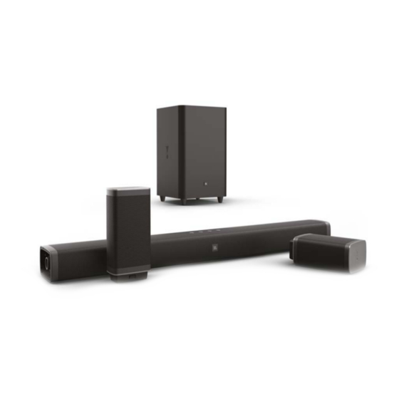
5.1-CHANNEL 4K ULTRA HD SOUNDBAR WITH TRUE WIRELESS SURROUND SPEAKERS
SKU: JBLBAR51BLKAM, JBLBAR51BLKEP, JBLBAR51BLKUK, JBLBAR51BLKAS, JBLBAR51BLKCN,
JBLBAR51BLKBR
JBLBAR51BLKBR
Released by Global Quality
CONTENTS
Safety Instruction ...................................................................................... 2
Technical Specifications ............................................................................ 5
Software upgrade Instruction & Reset Procedure .................................... 6
Troubleshooting Charts ............................................................................ 7
Disassembly Instruction ............................................................................ 8
Block Diagram.......................................................................................... 11
Wiring Diagram ........................................................................................ 12
Circuit Diagarms & PCBA Layout ............................................................ 13
Mechanical Exploded View .................................................................... 36
Ist . ..................................................................................... 40
Revision List ............................................................................................
harman/kardon, Inc.
Service Manual
Ver. 1.5 Dec./2019
Advertisement
Table of Contents

Related Manuals for Harman JBL BAR 5.1


Summary of Contents for Harman JBL BAR 5.1
- Page 1 Service Manual JBL BAR 5.1 5.1-CHANNEL 4K ULTRA HD SOUNDBAR WITH TRUE WIRELESS SURROUND SPEAKERS SKU: JBLBAR51BLKAM, JBLBAR51BLKEP, JBLBAR51BLKUK, JBLBAR51BLKAS, JBLBAR51BLKCN, JBLBAR51BLKBR JBLBAR51BLKBR CONTENTS Safety Instruction ..................2 Technical Specifications ................5 Software upgrade Instruction & Reset Procedure ........6 Troubleshooting Charts ................
- Page 2 NOTE: Changes or ations not expressly approved regarding the environmentally sound collection, recycling and by Harman could void the user’s authority to operate the disposal of used batteries. equipment. To remove the batteries from your equipment or remote...
- Page 3 ELECTROSTATICALLY SENSITIVE(ES) DEVICES Some semiconductor (solid state) devices can be damaged easily by static electricity. Such components commonly are called Electrostatically Sensitive (ES) Devices. Examples of typical ES devices are integrated circuits and some field effect transistors and semiconductor "chip" components. The following techniques should be used to help reduce the incidence of component damage caused by static electricity.
- Page 4 SAFETY PRECAUTIONS The following check should be performed for the continued protection of the customer and service technician. LEAKAGE CURRENT CHECK Measure leakage current to a known earth ground (water pipe, conduit, etc.) by connecting a leakage current tester between the earth ground and all exposed metal parts of the appliance (input/output terminals, screwheads, metal overlays, control shaft, etc.).
- Page 5 Bluetooth SIG, Inc. and any use of such marks by HARMAN International Industries, Incorporated is under license. Other trademarks and trade names are those of their respective owners.The terms HDMI, the HDMI logo, and High-Definition Multimedia Interface are trademarks or registered trademarks of HDMI Licensing LLC in the United States and other countries.
- Page 6 Software upgrade Instruction& Reset Procedure 1)Restore factory setting 1) Hold down < Volume + > ,< Source > ,< Volume - > keys on the top panel 2) Then,the unit will show “RESET” on LED Display to indicate the reset successful. 3) After factory settings restored, the unit will reboot automatically.
- Page 7 Trouble Shooting REPAIR CHART Power Supply No working Power Supply No working All Function No Working All Function No Sound AUX IN No Sound Bluetooth No Sound Optical In No Sound USB No Function HDMI IN Function No Sound No Sound Battery no Voltage Micro USB No Subwoofer No sound...
- Page 8 Dismantling of the CONNETOR PCBA Disassembly instruction(main unit) 1) Loosen 1 screw on the top of CONNETOR PCBA as shown in fi gure 6 Note:In some service positions the components or copper patterns of one board may risk touching its neighbouring pc boards or metallic parts.
- Page 9 Dismantling of the Metall Grill Dismantling of AMP&MAIN&REPEATER PCBA Dismantling of AMP&MAIN&REPEATER PCBA 1) Loosen 2 screws as shown in fi gure 17 to remove the END CAP RING & END CAP. 1) Loosen 2 screws at the bracket as shown in fi gure 11,then pull out the PCBA ASS’Y. 1) Loosen 2 screws at the bracket as shown in fi gure 11,then pull out the PCBA ASS’Y.
- Page 10 Dismantling of the MAIN PCBA DISASSEMBLY INSTRUCTIONS (Subwoofer) 1) Loosen 4 pcs screws at the Rear Housing as shown in fi gure 22 to remove the Main PCBA. Dismantling of the Real Panel ASS’Y 1) Loosen 8 pcs screws as shown in fi gure 27 to remove the Real Panel Ass’y. Figure 22 Dismantling of the INSERT COVER ASS’Y...
- Page 11 Block Diagram Main Unit Jack Optical detect CRYSTAL 3.5mm 24.576MHz Transistor TPA3118D2 Tweeter 6 ohm 25W / 1% OPTICAL Class D GPIO control 12 ohm // 12ohm AW9523B = 6 ohm 25W / 1% LRCK CS42528 ABCK Codec TPA3118D2 MCLK Tweeter 6 ohm 25W / 1% TAS5538 SDOUT...
- Page 12 Wiring Diagram Wireless Subwoofer Main Unit JK6002 JK6000 REPEATER PCBA JK6001 JK6003 SUB POWER PCBA CN6001 USB1000 JK1000 AMP PCBA CN902 MAIN PCBA CN7005 CN7003 CN7006 CN7001 CN5002 CN1003 CN1012 CN1013 CN1004 CN5004 SUB AMP PCBA JK5000 LD3000 CN1013B CN1014A WIRELESS PCBA CONNETOR PCB CN1012B...
- Page 13 Circuit Diagram-AMP PCBA PVCC L7000 10UH R7011 3.3R TO MAIN BOARD MCU&DSP C7046 C7020 684/63V C7058 CN7000 C7070 MODSEL PVCC 330P PDN_1 C7060 PVCC R7000 C7093 FAULTZ BSPR C7077 R7001 C7027 RINP OUTPR C7047 C7078 RINN R7012 684/63V PLIMIT PDN_1 OUTNR 3.3R C7094...
- Page 14 Layout Diagram Top View-AMP PCBA LRA112770-0201 R7040 C7118 R7039 R7042 C7112 C7115 R7041 R7026 R7023 C7091 C7094 C7093 L7001 R7000 C7111 R7001 C7021 C7041 R7005 C7045 R7006 C7043 C7042 R7048 C7044 C7040 C7025 C7092 C7100 C7102 C7099 R7013 C7052 L7007 C7131 L7003 C7061...
- Page 15 Layout Diagram Bottom View-AMP PCBA C7132 Q7007 R7052 R7055 Q7008 R7053 C7117 R7043 C7070 Q7005 C7017 CN7004 C7073 C7071 C7005 C7010 C7127 Q7001 R7032 Q7000 R7028 C7075 R7034 Q7003 C7074 C7072 C7104 C7008 C7006...
- Page 16 Circuit Diagram--DISP.+WIRELESS+CONV+JK PCBA JACK PCB LFA112613-0401 CN1003B JK1002 MIC SIG MIC DET JK_MIC 100P LD3000 CN3/125_SMD_H C1121 IC3000 IC_SM1616 SEG5 SEG4 SEG6 SEG3 R3010 R3000 SEG7 SEG2 D3000 L_5V DIG1 GRID0 R3011 R3001 DIG2 GRID1 SEG1 1N4148 R3002 DIG3 GRID2 SEG0 C3003 R3003...
- Page 17 Layout Bottom View Diagram--DISP.+WIRELESS+CONV+JK PCBA Layout Top View Diagram--DISP.+WIRELESS+CONV+JK PCBA DISPLAY PCB LD3000 D=1.6mmX2 R3010 R3011 C3003 C3001 R3015 R3012 DISPLAY PCB R3014 R3013 SN3000 C3005 C3004 R1290 R1288 R1198 R1199 C1272 C1175 R1289 R1200 R1201 R1233 CN1005...
- Page 18 Circuit Diagram--KEY+CONNETOR PBCA CN1014B POWER_KEY SOURCE_KEY VOL_UP VOL_DOWN GND_K CN6/10_SMT_L KEY PCB CONNETOR PCB CN1012B CN1014A GND_K1 CN6/125_SMD_V CN6/125_SMD_V...
- Page 19 Layout Top View Diagram--KEY+CONNETOR PBCA VOL- POWER SOURCE VOL+ KEY PCB TO K CONNETOR PCB CN1014A CN1012B TO M Layout Bottom View Diagram--KEY+CONNETOR PBCA...
- Page 20 Circuit Diagram--POWER PCBA R911 C955 R910 SIL006019-1000 1000P 1KV SBD20200PI L907 L-6UH +24V L905 CN902 SIL162002 D918 C948 BD901 221 1KV PJE0994L4-2210 T901 GBU1008UL C944 C954 222 630V C927 C926 PQ3230 100P 1KV 220U 450V R988 R909 R908 D912 D913 R907 1N4148 1N4148...
- Page 21 Layout Top View Diagram--POWER PCBA VER:A 20170703 LFP112550-0201 C923 T901 GT902 H901 R951 C945 C946 H903 L902 C917 NTC901 ZD906 C916 L905 Q901 C951 AC INPUT R915 R914 L907 C957 ZD905 H902 C918 L904 R960 C936 C933 T4AL 250V R952 GT904 C927 F901...
- Page 22 Circuit Diagram--MAIN+REPEATER PCBA JK1000 R1031 22 R1168620 IC101274LVC1G157 C1046 470P +3.3VD R1032 CODEC_MCLK R1257 4R7 DSP_CLK IC1008 R1005 SCP_CLK IC1002A R1345 HDMI_MCLK SCP_CLK R1206 IC1009 TP1562A +3.3V R1006 SCP_MOSI SCP1_CLK EXT_A19 R117697.6 L1001 2.2uH CLK_SW SCP_MOSI R1207 DMA0 LIN_L+ X_sw R1012 SCP_MISO SCP1_MOSI...
- Page 23 Layout Top View Diagram--MAIN+REPEATER PCBA R1002 USB1000 R1031 CN1010 C1253 C1131 C1019 C1018 R1032 R1001 Q1011 R1360 C1254 R1293 R1296 R1295 R1297 C1003 R1034 R1298 R1035 R1228 R1294 C1240 C1105 JK1000 C1238 R1188 R1066 C1045 C1225 C1077 C1227 R1067 R1064 IC1014 C1239 R1063...
- Page 24 Layout Bottom View Diagram--MAIN+REPEATER PCBA D1012 R1181 IC1004 R1383 R1382 C1097 C1074 R1160 R1218 R1003 R1217 R1213 R1179 FB1001 C1216 C1050 C1049 R1211 C1129 R1223 R1219 D1009 R1220 C1035 MAIN PCB FB1008 R1226 ZD1000 L1002 C1130 C1133 L1000 R1029 C1042 C1015 C1041 Q1023...
- Page 25 Circuit Diagram--WL R+WL L+KEY+LED+JK PCBA( FB_0805_100 FB8004 W3V3 R8088 W+3.3V WMCLK MCLK CN8014 R8090 W-LRCK LRCK_W R8091 W-BCK BCK_W W3V3 WMCLK W_DWHP83 RX R8092 33 W_DATA0 SDIO_W WDebug CN8009 R8079 White_LED R8128 100 LD8001 GPO_5 RX_LED/SDIO_X WA-SDA M3V3 LED_SOD2 R8084 GPO_4 WA-SCL R8129...
- Page 26 Layout Top View Diagram--WL R+WL L+KEY+LED+JK PCBA( Layout Bottom View Diagram--WL R+WL L+KEY+LED+JK PCBA( C8063 C8064 C8062 WIRELESS R PCB WIRELESS L PCB R8129 CN8009 JK PCB LD8002 CN8007 JK8001 JK PCB KEY PCB LED PCB CN8013 LD8001 LED PCB R8128 KEY PCB...
- Page 27 Circuit Diagram-- MAIN LR PCBA ( R8032 R8039 620 R8043 0 PVCC C8024 C8019 470P L8002 10UH R8019 C8026 R8031 R8210 R8192 C8124 OP3.3V R8048 33 R8045 97.6 SROUT_P R8193 C8125 C8001 IC8002 PCM5100 C8126 C8132 222 2.2uF C8134 C8127 C8133 222 CN8002 DVDD...
- Page 28 Layout Top View Diagram-- MAIN LR PCBA ( LRM112630-0001 15-JUL-2017 SPK+ C8059 C8110 WGND C8105 R8118 C8056 C8057 L8002 C8008 C8031 R8101 SPK- C8070 C8092 R8117 C8114 C8049 IC8013 R8116 R8078 C8137 IC8005 C8136 L8005 CN8005 C8058 LD8005 LD8004 CN8011 C8094 C8083 Q8015...
- Page 29 Layout Bottom View Diagram-- MAIN LR PCBA ( BAR CPDE R8149 R8150 R8151 R8154 D8004 Q8011 C8100 D8008 C8078 C8074 C8080 IC8010 LRM112631-0001 D8006 R8148 C8117 C8103 C8038 C8044 C8118 C8104 IC8004 C8144 C8051 C8143 Q8003 R8133 R8156 R8161 IC8008 R8160 Q8012 R8073...
- Page 30 Circuit Diagram--SUB AMP+LED&JK PCBA(SUBWOOFER) FB5000 BK3.3V FB_0805_100 CN5000 DWHP83 RX IC5000 W3.3V MCLK MCLK R5016 W_LRCK R5018 LRCK_W PWM_HPM_L- PWM_P_6 W_BCK R5019 BCK_W W_DWHP83 RX C5099 PWM_HPP_L+ PWM_M_6 W_DATA0 AW_ON/OFF R5020 SDIO_W IC5001 LED_W R5003 GPO_5 RX_LED/SDIO_X 104P R5050 PWM_HPM_R- PWM_P_5 C5025 R5008...
- Page 31 Layout Top View Diagram--SUB AMP+LED&JK PCBA(SUBWOOFER) O4.0 LFA112590-0201 FB5002 C5082 SUB+ SUB- Q5003 CN5002 C5074 L5004 R5046 C5093 IC5003 Q5002 R5082 C5092 R5081 L5002 R5042 C5054 R5086 R5088 R5084 R5041 R5085 C5019 C5072 R5074 C5058 C5055 CN5004 C5056 R5068 R5040 C5099 R5014 R5067...
- Page 32 Layout Bottom View Diagram--SUB AMP+LED&JK PCBA(SUBWOOFER)
- Page 33 Circuit Diagram--SUB POWER PCBA(SUBWOOFER) CY901 560P-400V L903 TSB000026-0018 D915 SF20A400HPI 20A 400V L-6uH SIL162002 TVCC L902 HVCC R956 C933 C936 M222P/630V 68K/2W R951 R960 CE901 CE902 T902 120U 450V 120U 450V D910 D911 D912 PQ3535 56/3W 471P-500V FS1M FS1M FS1M R957 C931 C932...
- Page 34 Layout Top View Diagram--SUB POWER PCBA(SUBWOOFER) P902 SINGLE CEM-1 L151xW125.5xT1.6mm 1.0oz>32um BLACK/BLACK CE901 CE902 P903 LABEL BK12V CY901 SGND ON/OFF SGND BD901 J902 T901 EASTECH SGND LF902 SGND C932 C903 SGND J905 P904 J903 CY902 C940 J901 L903 CY905 C938 CX902 Q905 CY904...
- Page 35 Layout Bottom View Diagram--SUB POWER PCBA(SUBWOOFER) FB901 D905 R927 R917 C901 R929 C909 R924 R922 R901 C905 R908 IC902 C942 D908 C904 R919 R925 R907 C906 R920 C912 C902 ZD903 R948 D901 ZD902 IC901 R903 ZD901 R951 C941 R961 R932 C937 C936 C923...
- Page 36 Mechanical Exploded View (Main Unit) Pos. No. Part Number Description ASL160001-0003 METAL GRILLE PART ASS'Y BAR5.1 FSB042000-0601 TW SPK DRIVER 20W BAR5.1 FSB032000-0C01 MIDDLE SPK DRIVER 20W BAR5.1 BPF106098-0001 MAIN FRONT SOURCING BAR5.1 BPB100097-0003 MAIN REAR HOUSING EMEA/AS/CN BAR5.1 BPB100097-0001 MAIN REAR HOUSING US BAR5.1 ABN112550-0001 POWER PCBA EMEA AS CN BAR5.1...
- Page 37 MECHANICAL EXPLODED VIEW (SURR. SPK L) SL19 BRF100186-0001 RUBBER FOOT C SILICONE BAR5.1 SL16 BRF100185-0001 RUBBER FOOT I SILICONE BAR5.1 SL13 ABN100831-0006 SURR SPK L INSERT COVER BAR5.1 SL12 BPY100024-0001 SURR SPK END CAP L RING BAR5.1 SL10 ABN100831-0001 SURR SPK L/R BTM COVE BAR5.1 BPA100069-0001 SURR SPK L REAR HOUSING BAR5.1 SL15...
- Page 38 MECHANICAL EXPLODED VIEW (SURR. SPK R) SR22 ABE112783-0001 KEY PCBA BAR5.1 SR21 ABE112781-0001 WIRELESS R PCBA BAR5.1 SR20 BPB120098-0001 SURR SPK BUTTON BAR5.1 SR19 BRF100186-0001 RUBBER FOOT C SILICONE BAR5.1 SR16 BRF100185-0001 RUBBER FOOT I SILICONE BAR5.1 SR14 ABE112632-0001 SURR SPK MAIN R PCBA BAR5.1 SR13 ABN100831-0009 SURR SPK R INSERT COVER BAR5.1...
- Page 39 MECHANICAL EXPLODED VIEW (SUBWOOFER) Part Number Description ABNSB1600-S003 SUBWOOFER ASS'Y EMEA BAR5.1 ABNSB1600-S002 SUBWOOFER ASS'Y ASIA BAR5.1 ABNSB1600-S004 SUBWOOFER ASS'Y CHINA BAR5.1 ABNSB1600-S001 SUBWOOFER ASS'Y US BAR5.1 ABNSB1600-S005 SUBWOOFER ASS'Y BRAZIL BAR5.1 ABNSB1600-S006 SUBWOOFER ASS'Y UK BAR5.1 FSB02B001-0301 WOOFER DRIVER BAR5.1 SW2+SW3+ SW4+SW5+ ABN100125-0057...
- Page 40 JBL Bar 5.1 Spare Parts List V1.4 Product Name Pos. No. Part Number Description BAR 5.1 MAIN UNIT ASL160001-0003 METAL GRILLE ASS'Y BAR5.1 BAR 5.1 MAIN UNIT BRT100025-0001 KEY BUTTON BAR5.1 BAR 5.1 MAIN UNIT ABE112601-0001 KEY PCBA BAR5.1 BAR 5.1 MAIN UNIT FSB042000-0601 TW SPK DRIVER 20W BAR5.1...
- Page 41 BAR 5.1 SURR. SPEAKER SL1,SR1 BPH100415-0001 SURR SPK WALL MOUNT BKT BAR5.1 BAR 5.1 SURR. SPEAKER SL4,SR4 FSB012000-0601 SPEAKER DRIVER 20W FULL RANGE BAR5.1 BAR 5.1 SURR. SPEAKER SL5,SR5 ABE112784-0001 LED PCBA BAR5.1 BAR 5.1 SURR. SPEAKER SL6,SR6 GSP100137-0001 SURR SPK METAL GRILL BAR5.1 BAR 5.1 SURR.
- Page 42 BAR 5.1 IC1020,IC1021 RCI001541-0001 IC 6P WB1541 SOT23-6L BAR5.1 IC1022,IC1025,I BAR 5.1 RCI008201-0002 IC 6P SY8201 SOT23 BAR5.1 C5003 BAR 5.1 IC1026 RCI003170-0001 IC 3P LM317K-TN3-R 1.3V-37V BAR5.1 BAR 5.1 IC1027 RCI034063-0006 IC 8P AP34063S8L SOP-8L BAR5.1 BAR 5.1 IC3000 RCI001616-0001 IC 28P SM1616 SOP28 BAR5.1 BAR 5.1...
- Page 43 BAR 5.1 TVR901 RPT050001-0040 VARISTOR 50A 560V BAR5.1 BAR 5.1 ZD1000 RCI001604-0001 IC 6P CABC16-04S SOT-23 BAR5.1 BAR 5.1 28,SL2,SR2 HSR053103-8070 WALL MOUNT SCREW BAR5.1 WMC200029-0001 MIC. 1~10V 2.2KR BAR5.1 BAR 5.1 BAR 5.1 VTA900030-0001 BT ANTENNA 200mm BAR5.1 BAR 5.1 WPA120083-0021 WIRELESS MODULE-RX BAR5.1 BAR 5.1...
- Page 44 KEY COMBINATION BEHAVIOR Action Button Pattern Indicator Volume+ & source & Long press >3s Reset to factory default in On Mode. (VFD shows Volume- RESET) Long press>3s when Volume + & Power Enter demo mode(VFD shows “DEMO”) AC plug in Long press >3s Trigger software upgrade, and the VFD shows Volume - &...
- Page 45 REVISION LIST Version 1.0 * Initial release. Sep. 2017 Version 1.1 * Add callouts number in exloded views and add some wires & update some P/Ns in parts list . Nov. 2017 Version 1.2 * Some P/Ns updated and add UK & Brazil versions in parts list . Jun. 2018 Version 1.3 * Add Wall Mount Guide and spare parts list updated.
Need help?
Do you have a question about the JBL BAR 5.1 and is the answer not in the manual?
Questions and answers