Table of Contents
Advertisement
Quick Links
Advertisement
Table of Contents

Related Manuals for MicroSys miriac MPX-S32G274A


Summary of Contents for MicroSys miriac MPX-S32G274A
- Page 1 MPX-S32G274A User Manual (HW Revision 2) V2.1...
-
Page 2: Table Of Contents
ADC ..............33 10.4 Pin Definitions – Bottom ........68 4.12.5 CAN ..............34 10.5 4.12.6 RGMII..............34 10.6 Pins not available for pin multiplexing...75 4.12.7 ULPI (USB) ............35 miriac MPX-S32G274A User Manual V2.1 2/76 © MicroSys Electronics GmbH 2020... -
Page 3: General Notes
MicroSys Electronics GmbH f urther reserves the right to alter the layout and/or design of the hardware without prior notif ication and accepts no liability f or doing... -
Page 4: Offer To Provide Source Code Of Certain Software
This of f er is valid to anyone in receipt of this inf ormation. MicroSys Electronics GmbH is eager to duly provide complete source code as required under various Free Open Source Sof tware licenses. If however you... -
Page 5: Symbols, Conventions And Abbreviations
/ xxx_P denotes the positive signal of a differential pair denotes an optional not mounted or fitted part Table 2 Conventions miriac MPX-S32G274A User Manual V2.1 5/76 © MicroSys Electronics GmbH 2020... -
Page 6: Safety And Handling Precautions
There is no separate SHIELD connection. The module’s mounting holes are not connected to GND Take this into account when handling and mounting the unit. Table 3 Safety and Handling Precautions miriac MPX-S32G274A User Manual V2.1 6/76 © MicroSys Electronics GmbH 2020... -
Page 7: Short Description
Short Description The miriac MPX-S32G274A is a member of the MPX module f amily based on NXP’s S32G274A network processor (SoC). MicroSys Electronics GmbH of f ers a Development Kit which uses the key f eatures of the module. The customer can: ■... -
Page 8: System Description
■ Voltage regulators f or onboard voltages Ordering Information Ordering inf ormation can be f ound on the f ollowing website miriac MPX-S32G274A or contact your local sales representative. miriac MPX-S32G274A User Manual V2.1 8/76 © MicroSys Electronics GmbH 2020... -
Page 9: Power Consumption
With this inf ormation a cooling method needs to be designed which considers the f inal use case. If desired, MicroSys Electronics GmbH can support you with your cooling concept. Please ask your sales representative or send an email inquiry to support@microsys.de. -
Page 10: Technical Description
SD_D2 SD_D3 VCC_SDHC_1V8/3V3 PMIC_FCCU1_OUT RGMII2_MDC/DSPI0_CS7 RGMII2_MDIO RGMII2_RXD3/USB_D7 RGMII2_RXD2/USB_D6 RGMII2_RXD1/USB_D5 RGMII2_RXD0/USB_D4 RGMII2_RXDV/USB_D3 miriac MPX-S32G274A User Manual V2.1 10/76 © MicroSys Electronics GmbH 2020... - Page 11 RGMII1_TXD1 RGMII1_TXD0 RGMII1_TX_EN RGMII1_TX_CLK RGMII0_MDC RGMII0_MDIO RGMII0_RXD3 RGMII0_RXD2 RGMII0_RXD1 RGMII0_RXD0 miriac MPX-S32G274A User Manual V2.1 11/76 © MicroSys Electronics GmbH 2020...
- Page 12 RGMII0_TXD2 RGMII0_TXD1 RGMII0_TXD0 RGMII0_TX_EN RGMII0_TX_CLK PCIE1_RX0_N PCIE1_RX0_P PCIE1_RX1_N PCIE1_RX1_P PCIE0_RX0_N PCIE0_RX0_P PCIE0_RX1_N PCIE0_RX1_P CLK_OUT_N CLK_OUT_P PCIE1_TX0_N PCIE1_TX0_P PCIE1_TX1_N PCIE1_TX1_P PCIE0_TX0_N PCIE0_TX0_P miriac MPX-S32G274A User Manual V2.1 12/76 © MicroSys Electronics GmbH 2020...
- Page 13 T114 PB15 T115 PC00 T116 T117 +VREF1 T118 +VREF2 T119 +VREF3 T120 +VREF4 T121 T122 PCIE0_CLKIN_N T123 PCIE0_CLKIN_P T124 T125 T126 PMIC_RST# T127 RSTIN# T128 RST# miriac MPX-S32G274A User Manual V2.1 13/76 © MicroSys Electronics GmbH 2020...
- Page 14 T141 T142 T143 T144 T145 T146 +VIN T147 +VIN T148 +VIN T149 +VIN T150 +VIN T151 +VIN T152 +VIN T153 +VIN T154 +VIN Table 6 Module connector: top pins miriac MPX-S32G274A User Manual V2.1 14/76 © MicroSys Electronics GmbH 2020...
-
Page 15: Module Connector - Bottom Pins
ADC_CH_01 ADC_CH_00 CAN00_RX (INPUT) CAN00_TX CAN01_RX (INPUT) CAN01_TX CAN02_RX (INPUT) CAN02_TX CAN03_RX (INPUT) CAN03_TX CAN04_RX (INPUT) CAN04_TX miriac MPX-S32G274A User Manual V2.1 15/76 © MicroSys Electronics GmbH 2020... - Page 16 CAN12_TX CAN13_RX (INPUT) CAN13_TX CAN14_RX (INPUT) CAN14_TX CAN15_RX (INPUT) CAN15_TX PA15_DSPI0_SOUT PA13_DSPI0_SCK miriac MPX-S32G274A User Manual V2.1 16/76 © MicroSys Electronics GmbH 2020...
- Page 17 FLXR0A_TXEN# FLXR0B_RX_D FLXR0B_TX_D FLXR0B_TXEN# PB12_FXCAN2_RX B100 PB11_FXCAN2_TX B101 B102 PB14_FXCAN3_RX B103 PB13_FXCAN3_TX B104 miriac MPX-S32G274A User Manual V2.1 17/76 © MicroSys Electronics GmbH 2020...
- Page 18 B131 PC10_UART0_RX B132 B133 PB01_I2C0_SCL B134 PB00_I2C0_SDA B135 PB03_I2C1_SCL B136 PB04_I2C1_SDA B137 PB05_I2C2_SCL B138 PB06_I2C2_SDA B139 B140 miriac MPX-S32G274A User Manual V2.1 18/76 © MicroSys Electronics GmbH 2020...
- Page 19 B143 B144 B145 B146 B147 B148 +VIN B149 +VIN B150 +VIN B151 +VIN B152 +VIN B153 +VIN B154 +VIN B155 +VIN B156 +VIN Table 7 Module connector: bottom pins miriac MPX-S32G274A User Manual V2.1 19/76 © MicroSys Electronics GmbH 2020...
-
Page 20: Power Structure
Reference voltage output T133 VCC_RTC 0.9V-5.5V Optional backup supply Optional boot EEPROM pro- T134 +3V3_EXT 3.3V gramming supply input B125 VDD_OTP Do not connect Table 8 Module connector: power pin assignments miriac MPX-S32G274A User Manual V2.1 20/76 © MicroSys Electronics GmbH 2020... -
Page 21: Reset Structure
Open Drain PMIC_RST# System Global Reset Output Open Drain PORST# Power-On Reset for SoC DDR_RST# Reset for LPDDR Memory EMMC_RST# Reset for eMMC Memory Table 4-3 Reset signal overview miriac MPX-S32G274A User Manual V2.1 21/76 © MicroSys Electronics GmbH 2020... -
Page 22: Clock Structure
Signal Signal Signal I/O Range Frequency conditioning SR: 33R → CLK0+ AB15 PCIE0_CLK_P HCSL 100/125 MHz PD: 49R9 SR: 33R → CLK0- AC15 PCIE0_CLK_N HCSL 100/125 MHz PD: 49R9 miriac MPX-S32G274A User Manual V2.1 22/76 © MicroSys Electronics GmbH 2020... - Page 23 SR: 33R → CLK1+ AB16 PCIE1_CLK_P HCSL 100/125 MHz PD: 49R9 SR: 33R → CLK1- AC16 PCIE1_CLK_N HCSL 100/125 MHz PD: 49R9 Table 11 PCIE1 clock: pin assignments miriac MPX-S32G274A User Manual V2.1 23/76 © MicroSys Electronics GmbH 2020...
- Page 24 RGMII2_TX_ → +VREF2 SR: 10R 125 MHz RGMII2_RX_ RGMII2_RX_ ← +VREF2 SR: 10R 125 MHz → RGMII2_MDC RGMII2_MDC +VREF2 SR: 10R < 10 MHz Table 12 Clock: pin assignments miriac MPX-S32G274A User Manual V2.1 24/76 © MicroSys Electronics GmbH 2020...
-
Page 25: Boot Mode Configuration
BOOT_CFG1[7:5] conf igures the boot devices: Boot BOOT_CFG1[7:5] Boot Source Description Location Quad/Hyper/Octal Flash QuadSPI Boot Module (see BOOT_CFG[4:2]) SD Boot SD Card Carrier eMMC eMMC Boot Module Table 15 Boot devices miriac MPX-S32G274A User Manual V2.1 25/76 © MicroSys Electronics GmbH 2020... -
Page 26: Leds
Reset is inactive LED ON: Peripheral reset is active LED OFF: Reset is inactive LED ON: User defined function Yellow LED OFF: User defined function Table 16 LED: pin description miriac MPX-S32G274A User Manual V2.1 26/76 © MicroSys Electronics GmbH 2020... -
Page 27: Rtc
The RTC’s interrupt output is connected to the GPIO Expander: GPIO Expander PCF85263ATL Signal Signal Signal Range conditioning ← RTC_IRQA# INTA# +VREF3 PU: 4k7 ← RTC_IRQB# INTB# +VREF3 PU: 4k7 Table 18 RTC: IRQs miriac MPX-S32G274A User Manual V2.1 27/76 © MicroSys Electronics GmbH 2020... -
Page 28: Temperature Sensor
The temperature sensor provides two interrupts which are connected to the GPIO Expander: GPIO Expander TMP451 Signal Signal I/O Range Signal conditioning ← THERM_ALERT# ALERT#/THERM2 +VREF3 PU: 4k7 ← THERM_FAULT# THERM# +VREF3 PU: 4k7 Table 19 Temperature sensor: IRQs miriac MPX-S32G274A User Manual V2.1 28/76 © MicroSys Electronics GmbH 2020... -
Page 29: Gpio Expander
Hardware Revision 7 Hardware Revision 8 Table 21 GPIO Expander: Hardware Revision S32G274A GPIO Expander Ball Signal Signal Signal conditioning ← PU: 10k PC13 EXPD_IRQ# Table 22 GPIO Expander: IRQ miriac MPX-S32G274A User Manual V2.1 29/76 © MicroSys Electronics GmbH 2020... -
Page 30: Serial Boot Eeprom (Rcon)
DIP Switch: • SD-Card • eMMC Boot from J4 configuration SD card SD-Card • SD-Card DIP Switch: • SD-Card • eMMC • eMMC • SPI NOR Table 23 Boot configuration miriac MPX-S32G274A User Manual V2.1 30/76 © MicroSys Electronics GmbH 2020... -
Page 31: Electronic Dip Switch
MUX_OUT = EEPROM BYTE 0 1 (DEFAULT) MUX_OUT = MUX_IN Table 24 Electronic DIP Switch: MUX_OUT after POR Initial EEPROM programming is done during production test and can be overridden via I2C. miriac MPX-S32G274A User Manual V2.1 31/76 © MicroSys Electronics GmbH 2020... - Page 32 J1: W10) = 0 Bootmode Pin 1 ( J1: W11) = 1 Bootmode Pin 2 ( PA03_BOOTMOD2 W11) = 0 Bootmode Pin 2 (J1: Table 26 Electronic DIP Switch: MUX_IN / MUX_OUT miriac MPX-S32G274A User Manual V2.1 32/76 © MicroSys Electronics GmbH 2020...
-
Page 33: Interface Description
The terms “primary”, “secondary”, … do not imply any priority. The connector’s pin names are derived f rom the primary f unctions def ined by MicroSys. Primary interf aces can be also be conf igured f or other interf aces. Nevertheless, high speed interf aces are optimized in layout, signals are length and of ten group matched. -
Page 34: Can
USB_D6 RGMII2_RXD1 USB_D5 RGMII2_RXD0 USB_D4 RGMII2_RXDV USB_D3 RGMII2_RX_CLK USB_D2 RGMII2_TXD3 USB_D1 RGMII2_TXD2 USB_D0 RGMII2_TXD1 USB_NXT RGMII2_TXD0 USB_STP RGMII2_TX_EN USB_DIR RGMII2_TX_CLK USB_CLK Table 27 RGMII2 / ULPI pin multiplexing options miriac MPX-S32G274A User Manual V2.1 34/76 © MicroSys Electronics GmbH 2020... -
Page 35: Ulpi (Usb)
(slave address) Temperature Sensor TMP451 (General Call reset 0x00 address) DIP Switch PCA9561PW 0x4D EEPROM AT24C01C-SSHM 0x50 PCF85263ATL 0x51 EEPROM BR24G128NUX-3 0x54 EEPROM AT24C01C-SSHM 0x56 Table 28 I2C0: bus map miriac MPX-S32G274A User Manual V2.1 35/76 © MicroSys Electronics GmbH 2020... - Page 36 I2C 3 is available by multiplexing functions. Primary interface is FlexCAN3. I2C4 map: Device Addr PMIC VR5510 Main logic 0x20 PMIC VR5510 Fail-safe logic 0x21 Table 31 I2C4: bus map miriac MPX-S32G274A User Manual V2.1 36/76 © MicroSys Electronics GmbH 2020...
-
Page 37: Qspi (Flash)
1.8V ↔ QSPI1_A_DATA3 1.8V ↔ QSPI1_A_DATA4 1.8V ↔ QSPI1_A_DATA5 1.8V ↔ QSPI1_A_DATA6 1.8V ↔ QSPI1_A_DATA7 1.8V B4, E4, D1 +1.8V PU 1.8V Table 32 QSPI NOR Flash: pin assignments miriac MPX-S32G274A User Manual V2.1 37/76 © MicroSys Electronics GmbH 2020... -
Page 38: Spi
The MPX-S32G274A has 1 LLCE FlexRay interf ace with dual channels as primary interf ace and another shared FlexRay interf ace due to pin multiplexing. The pins are listed in the Appendix in chapter 10.4 and 10.5. miriac MPX-S32G274A User Manual V2.1 38/76... -
Page 39: Sdhc
“VCC_SDHC_1V8/3V3“ is a ref erence voltage which indicates the level of the sup- ply voltage of the SDHC interf ace: Module Connector Ball Signal Signal I/O Range Signal conditioning VCC_SDHC_1V8/ VCC_SDHC_1V8/ → 1.8V / 3.3V miriac MPX-S32G274A User Manual V2.1 39/76 © MicroSys Electronics GmbH 2020... -
Page 40: Serdes
However, root complex (RC) or endpoint (EP) mode is determined via sof tware. Signal Signal Conditioning Function S32G274A is endpoint (clock from carrier) T130 SEL_CLK_RC/EP# PU: 10k S32G274A is root complex (clock from module) Table 36 SerDes: root complex / endpoint miriac MPX-S32G274A User Manual V2.1 40/76 © MicroSys Electronics GmbH 2020... - Page 41 Figure 4-8 SerDes: clock routing miriac MPX-S32G274A User Manual V2.1 41/76 © MicroSys Electronics GmbH 2020...
-
Page 42: Mechanical Description
The MPX-S32G274A module has 314 edge f inger contacts. Appropriate sockets on the carrier provide 314 pins with 0.5mm pitch and accept edge cards with a thickness of 1.2mm. miriac MPX-S32G274A User Manual V2.1 42/76 © MicroSys Electronics GmbH 2020... -
Page 43: Previous Numbering Scheme
OBSOLETE. 314-pin connectors have pins between B9/B10 and T9/T10 which are now connected on the module! They are called “top key” and “bottom key” pins TK1, TK2, BK1, BK2. miriac MPX-S32G274A User Manual V2.1 43/76 © MicroSys Electronics GmbH 2020... -
Page 44: Pin-Layout
“B1”, … ”B9”, ”BK1“, ”BK2“, ”B10“, … ”B155”, “B156” Bottom “T1”, … ”T9”, ”TK1“, ”TK2“, ”T10“, … “T153”, “T154“ Table 37 Connector pin naming scheme Figure 5-2 Connector orientation miriac MPX-S32G274A User Manual V2.1 44/76 © MicroSys Electronics GmbH 2020... - Page 45 The module connector is usually used f or MXM3 graphic cards commonly f ound in notebooks. MicroSys changed the pin layout so that all 314 physically available pins can be used. Alternatives - there are several connectors on the market that can be used if there are no conf licts with the mechanical dimensions of the module.
-
Page 46: 5.5 Mounting/Unmounting
Lif t the module to about 25° and remove it f rom the connector. Store the parts on a static f ree area. miriac MPX-S32G274A User Manual V2.1 46/76... -
Page 47: Board Outline
The f ollowing drawing shows the mechanical outline (82x50mm) of the MPX-S32G274A module: Figure 5-4 Board dimensions The mounting holes require M2.5 screws. For 3D data files please contact MicroSys. miriac MPX-S32G274A User Manual V2.1 47/76 © MicroSys Electronics GmbH 2020... -
Page 48: Height
Depends on connector type DIM. E Connector product height Depends on connector type Table 39 Construction height overview Thickness The PCB thickness of the MPX-S32G274A module is 1.2mm ± 10%. miriac MPX-S32G274A User Manual V2.1 48/76 © MicroSys Electronics GmbH 2020... -
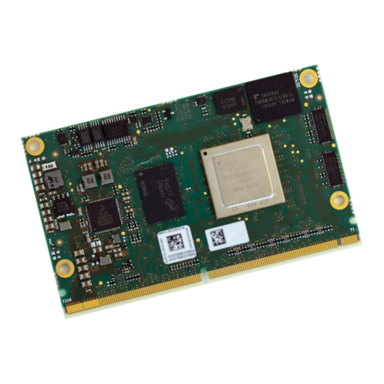
Page 49: Component Layout - Top Side
Component Layout - Top Side Figure 5-6 Top Components miriac MPX-S32G274A User Manual V2.1 49/76 © MicroSys Electronics GmbH 2020... - Page 50 Memory Primary Serial RCON EEPROM eMMC Memory Electronic DIP switch Serial NOR Flash Memory Secondary Serial RCON EEPROM TMP451 Temperature sensor GPIO Expander EEPROM Table 40 Top side components miriac MPX-S32G274A User Manual V2.1 50/76 © MicroSys Electronics GmbH 2020...
-
Page 51: Component Layout - Bottom Side
Component Layout – Bottom Side 5.10 Figure 5-7 Bottom components miriac MPX-S32G274A User Manual V2.1 51/76 © MicroSys Electronics GmbH 2020... - Page 52 Type Function Part Reference PI6C557 Clock Generator PI6C557 Clock Generator PCF85263ATL LD1, LD2, LD3, LD4 Side Looker LED Reset, Power, User LED Table 41 Components on bottom miriac MPX-S32G274A User Manual V2.1 52/76 © MicroSys Electronics GmbH 2020...
-
Page 53: Software
LPDDR4 conf iguration and timing Operating System MicroSys Electronics GmbH of f ers Linux support f or the module. Please ref er to the MicroSys Sof tware Enablement Guide f or more details. Other Operating Systems are available on request only. -
Page 54: Safety Requirements And Protective Regulations
The MPX-S32G274A is designed to withstand a high level of vibration and shock since there are no heavy and no overhanging components on the module. If desired, MicroSys Electronics GmbH can support you with your shock and vibration concept. Please ask your sales representative or send an email inquiry to support@microsys.de. -
Page 55: Climatic Conditions
The relative humidity during operation or storage of the module may not exceed 10% to 90%, non-condensing. RoHS All components on the MPX-S32G274A are RoHS compliant, also a RoHS compliant soldering process is used f or manuf acturing. miriac MPX-S32G274A User Manual V2.1 55/76 © MicroSys Electronics GmbH 2020... -
Page 56: General Notes
. The manuf acturer’s advice should be f ollowed. If desired, MicroSys Electronics GmbH can support you with your lif ecycle management regarding chip errata. Please ask your sales representative or send an email inquiry to support@microsys.de. -
Page 57: History
I2C address of serial RCON changed to 0x56 Revised chapter “interface description” Changed supply voltage for SDHC interface Swapped “PC11” and “PC12” on connector pins “B19”/”B20” 2021-06-15 Table 42 Document history miriac MPX-S32G274A User Manual V2.1 57/76 © MicroSys Electronics GmbH 2020... -
Page 58: Appendix
SerDes......................Serializer Deserializer SoC ........................System on a Chip SoM........................System on Module SPI......................Serial Peripheral Interface UART ..............Universal Asynchronous Receiver Transmitter ULPI ......................UTMI+ Low Pin Interface USB......................... Universal Serial Bus miriac MPX-S32G274A User Manual V2.1 58/76 © MicroSys Electronics GmbH 2020... -
Page 59: Table Of Figures
Figure 5-4 Module (un)mounting..................... 46 Figure 5-5 Board dimensions......................47 Figure 5-7 Construction height for parts ..................48 Figure 5-8 Top Components ......................49 Figure 5-9 Bottom Components ...................... 51 miriac MPX-S32G274A User Manual V2.1 59/76 © MicroSys Electronics GmbH 2020... -
Page 60: Table Of Tables
Table 38 Connector Types: Ordering Information ................ 45 Table 39 Construction height overview ..................48 Table 40 Top side components ....................... 50 Table 41 Bottom side components ....................52 Table 42 Document history ......................57 miriac MPX-S32G274A User Manual V2.1 60/76 © MicroSys Electronics GmbH 2020... -
Page 61: 10.4 Pin Definitions - Top
Power / SDHC PMIC_FCCU1_OUT J2-31 CTRL +VREF4 (3V3) 5k11 RGMII2_MDC/DSPI0_CS7 PF00 RGMII +VREF1 (1V8) RGMII2_MDIO PF01 RGMII INOUT +VREF1 (1V8) RGMII2_RXD3/USB_D7 PH00 RGMII / ULPI IN / INOUT +VREF1 (1V8) miriac MPX-S32G274A User Manual V2.1 61/76 © MicroSys Electronics GmbH 2020... - Page 62 PE13 RGMII +VREF1 (1V8) RGMII1_RXD2 PE12 RGMII +VREF1 (1V8) RGMII1_RXD1 PE11 RGMII +VREF1 (1V8) RGMII1_RXD0 PE10 RGMII +VREF1 (1V8) RGMII1_RXDV PE09 RGMII +VREF1 (1V8) RGMII1_RX_CLK PE08 RGMII +VREF1 (1V8) miriac MPX-S32G274A User Manual V2.1 62/76 © MicroSys Electronics GmbH 2020...
- Page 63 PH03 RGMII +VREF1 (1V8) RGMII0_TXD2 PH02 RGMII +VREF1 (1V8) RGMII0_TXD1 PH01 RGMII +VREF1 (1V8) RGMII0_TXD0 PJ00 RGMII +VREF1 (1V8) RGMII0_TX_EN PE14 RGMII +VREF1 (1V8) RGMII0_TX_CLK PH10 RGMII +VREF1 (1V8) miriac MPX-S32G274A User Manual V2.1 63/76 © MicroSys Electronics GmbH 2020...
- Page 64 SERDES +VREF1 (1V8) 220nF PCIE1_TX1_N SERDES +VREF1 (1V8) 220nF PCIE1_TX1_P SERDES +VREF1 (1V8) 220nF PCIE0_TX0_N SERDES +VREF1 (1V8) 220nF PCIE0_TX0_P SERDES +VREF1 (1V8) 220nF PCIE0_TX1_N SERDES +VREF1 (1V8) 220nF miriac MPX-S32G274A User Manual V2.1 64/76 © MicroSys Electronics GmbH 2020...
- Page 65 INOUT +VREF3 (3V3) T115 PC00 PC00 GPIO INOUT +VREF3 (3V3) T116 T117 +VREF1 POWER 1V8 Reference Output T118 +VREF2 POWER 1V8 Reference Output T119 +VREF3 POWER 3V3 Reference Output miriac MPX-S32G274A User Manual V2.1 65/76 © MicroSys Electronics GmbH 2020...
- Page 66 Module Input (0.9V - 5.5V) Programming Voltage: T134 +3V3_EXT PRODUCTION Module Input (3.3V ± 5%) T135 I2C_SCL_PROG J9-7 PRODUCTION +3V3_EXT T136 I2C_SDA_PROG J9-6 PRODUCTION INOUT +3V3_EXT T137 T138 T139 T140 T141 T142 miriac MPX-S32G274A User Manual V2.1 66/76 © MicroSys Electronics GmbH 2020...
- Page 67 9-30V T148 +VIN POWER 9-30V T149 +VIN POWER 9-30V T150 +VIN POWER 9-30V T151 +VIN POWER 9-30V T152 +VIN POWER 9-30V T153 +VIN POWER 9-30V T154 +VIN POWER 9-30V miriac MPX-S32G274A User Manual V2.1 67/76 © MicroSys Electronics GmbH 2020...
-
Page 68: 10.5 Pin Definitions - Bottom
+VREF1 (1V8) ADC_CH_07 +VREF1 (1V8) ADC_CH_06 +VREF1 (1V8) PMIC_STBY# J2-2 CTRL +VREF4 (3V3) PMIC_VDD_OK J2-4 CTRL +VREF4 (3V3) ADC_CH_05 +VREF1 (1V8) ADC_CH_04 +VREF1 (1V8) ADC_CH_03 +VREF1 (1V8) ADC_CH_02 +VREF1 (1V8) miriac MPX-S32G274A User Manual V2.1 68/76 © MicroSys Electronics GmbH 2020... - Page 69 PJ08 +VREF3 (3V3) CAN04_TX PJ07 CAN05_RX +VREF4 (3V3) PJ10 CAN05_TX +VREF3 (3V3) PJ09 CAN06_RX +VREF4 (3V3) PJ12 CAN06_TX +VREF3 (3V3) PJ11 +VREF4 (3V3) CAN07_RX PJ14 CAN07_TX +VREF3 (3V3) PJ13 miriac MPX-S32G274A User Manual V2.1 69/76 © MicroSys Electronics GmbH 2020...
- Page 70 PK07 CAN13_RX +VREF4 (3V3) PK10 CAN13_TX +VREF3 (3V3) PK09 +VREF4 (3V3) CAN14_RX PK12 CAN14_TX +VREF3 (3V3) PK11 +VREF4 (3V3) CAN15_RX PK14 CAN15_TX +VREF3 (3V3) PK13 PA15_DSPI0_SOUT +VREF3 (3V3) PA15 miriac MPX-S32G274A User Manual V2.1 70/76 © MicroSys Electronics GmbH 2020...
- Page 71 JCOMP +VREF3 (3V3) JTAG PF03_CLKOUT0 +VREF1 (1V8) PF03 CLOCK +VREF1 (1V8) PF04_CLKOUT1 PF04 CLOCK FLXR0A_RX_D +VREF4 (3V3) PL03 FLEXRAY FLXR0A_TX_D +VREF3 (3V3) PL02 FLEXRAY FLXR0A_TXEN# +VREF3 (3V3) PL01 FLEXRAY miriac MPX-S32G274A User Manual V2.1 71/76 © MicroSys Electronics GmbH 2020...
- Page 72 B112 PC05 B113 LIN3_RX +VREF4 (3V3) B114 PL07 +VREF3 (3V3) B115 LIN3_TX PC07 B116 PCIE1_CLKC_N J16-14 SERDES +VREF4 (3V3) 49R9 B117 J16-15 SERDES +VREF4 (3V3) 49R9 B118 PCIE1_CLKC_P B119 miriac MPX-S32G274A User Manual V2.1 72/76 © MicroSys Electronics GmbH 2020...
- Page 73 INOUT +VREF3 (3V3) B135 PB03_I2C1_SCL PB03 +VREF3 (3V3) B136 PB04_I2C1_SDA PB04 INOUT +VREF3 (3V3) B137 PB05_I2C2_SCL PB05 +VREF3 (3V3) B138 PB06_I2C2_SDA PB06 INOUT B139 B140 B141 B142 B143 B144 miriac MPX-S32G274A User Manual V2.1 73/76 © MicroSys Electronics GmbH 2020...
- Page 74 +VIN Power 9-30V B150 +VIN Power 9-30V B151 +VIN Power 9-30V B152 +VIN Power 9-30V B153 +VIN Power 9-30V B154 +VIN +VIN Power 9-30V B155 +VIN Power 9-30V B156 miriac MPX-S32G274A User Manual V2.1 74/76 © MicroSys Electronics GmbH 2020...
-
Page 75: 10.6 Pins Not Available For Pin Multiplexing
SDC / eMMC PD09 SDC / eMMC PD10 SDC / eMMC PG00 QSPI PG01 QSPI PG02 QSPI PG03 QSPI PG04 QSPI PG05 QSPI PF05 QSPI PF06 QSPI PF07 QSPI miriac MPX-S32G274A User Manual V2.1 75/76 © MicroSys Electronics GmbH 2020... - Page 76 QSPI PF12 QSPI PF13 QSPI PF14 QSPI PA02 PA02_BOOTMOD1 CONFIG PA03 PA03_BOOTMOD2 CONFIG PB00 PB00_I2C0_SDA PB01 PB01_I2C0_SCL PC01 PC01_I2C4_SDA_PMIC PC02 PC02_I2C4_SCL_PMIC PC03 PMIC_IRQ# CONFIG PC13 PC13 PD11 PMIC_FS0# CONFIG miriac MPX-S32G274A User Manual V2.1 76/76 © MicroSys Electronics GmbH 2020...
Need help?
Do you have a question about the miriac MPX-S32G274A and is the answer not in the manual?
Questions and answers