
Related Manuals for Mobiletek LYNO L306

Summary of Contents for Mobiletek LYNO L306
- Page 1 L306 Hardware Design L306 Hardware Design GSM/WCDMA Module Series Version: V1.8 Date: 2018-03-06 Copyright © Shanghai Mobiletek Communication Ltd Shanghai Mobiletek Communication Ltd...
- Page 2 Thus, the descriptions herein may not exactly match the product or its accessories which you purchase. Shanghai Mobiletek Communication Ltd reserves the right to change or modify any information or specifications contained in this manual without prior notice and without any liability.
- Page 3 Modify chapter “storage and production”; add label 2017-10-10 V1.7 Rc.dong description; delete SD card and SPI, update Log Add differences between L306E/A and L306G; 2018-03-06 V1.8 modify description of the PIN59 and PIN82; update Rc.dong Figure 3-9 and Figure 3-10 Copyright © Shanghai Mobiletek Communication Ltd...
-
Page 4: Table Of Contents
Electrical characteristics ......................... 32 4.1 Electrical characteristics ....................... 32 4.2 Temperature characteristic ......................32 4.3 Absolute Maximum Power ......................33 4.4 Recommended operating conditions .................... 33 4.5 Power consumption........................33 4.6 Power Sequence.......................... 35 Copyright © Shanghai Mobiletek Communication Ltd... - Page 5 6.2 Production ........................... 44 6.2.1 Module confirmation and moisture ..................45 6.2.2 SMT reflow attentions ......................46 6.2.3 SMT stencil design and the problem of less tin soldering ............47 6.2.4 SMT attentions ........................47 Copyright © Shanghai Mobiletek Communication Ltd...
-
Page 6: Introduction
L306 is a small UMTS/HSPA+ module for LCC package, with stable and reliable performance. It supports UMTS/HSDPA/HSUPA900(850)/2100(1900) and can be completely compatible with existing GSM/GPRS/EDGE networks. 1.1 Hardware Diagram Figure 1-1 L306 functional architecture 1.2 Main features ARM Cortex-R4@481MHz Copyright © Shanghai Mobiletek Communication Ltd... -
Page 7: Specifications
● ● HSPA HSUPA ● ● ● 1.3 Specifications Supply Voltage Range:3.3~4.2V(type3.8V) Dimensions:30mm * 30mm * 2.65mm Package:94-pin LCC Operation Temperature Range:-40℃~+85℃ Storage Temperature Range:-45℃~+90℃ Antenna:Main Antenna、Diversity Antenna Copyright © Shanghai Mobiletek Communication Ltd... -
Page 8: Interfaces
L306 Hardware Design Weight :Approx 5g 1.4 Interfaces PCM: Digital audio interface SIM: Support 1.8V/3V UART: High speed UART USB 2.0: High Speed ,480Mbps Copyright © Shanghai Mobiletek Communication Ltd... -
Page 9: Package Information
G N D U S I M _ C L K U S I M _ VCC G N D G N D AN T 2 Power Other UART Figure 2-1 L306 Pin View Copyright © Shanghai Mobiletek Communication Ltd... -
Page 10: Pin Definition
UART1 TX DVDD18 Open GPIO50 General input/output PIN DVDD18 Open Ground USB_DM Open USB port differential data line USB_DP Open Ground VIO18 1.8V output voltage 1.8V Open LPRDB USB download key (Reserve) DVDD18 Open Copyright © Shanghai Mobiletek Communication Ltd... - Page 11 Open USIM_CLK USIM clock DVDD18 Open USIM_VCC USIM output voltage 1.8/3.0V Open GPIO39 General input/output PIN DVDD18 Open GPIO30 General input/output PIN DVDD18 Open Ground VBAT VBAT 3.3~4.2V Power supply VBAT VBAT Ground Ground Copyright © Shanghai Mobiletek Communication Ltd...
- Page 12 General input/output PIN. It can be GPIO49 DVDD18 Open used as IIC data Ground Ground Pin number L306E/A L306G Pin59 Main_ANT ANT1 Open Main_A Pin82 MIMO_ANT Ground Ground VBAT VBAT 3.3~4.2V Power supply VBAT VBAT Ground Ground Copyright © Shanghai Mobiletek Communication Ltd...
- Page 13 PCM_SYNC PCM interface sync DVDD18 Open PCM_CLK PCM interface clock DVDD18 Open Ground Ground Ground Ground Pin number L306E/A L306G Pin59 Main_ANT ANT2 Open Main_A Pin82 MIMO_ANT Ground Ground Ground Ground Ground Ground Ground Copyright © Shanghai Mobiletek Communication Ltd...
-
Page 14: Package Information
P:POWER G:GROUND I:INPUT DI:DIGITAL INPUT O:OUTPUT DO:DIGITAL OUTPUT ANT:ANTENNA DIO:DIGITAL INPUT OUTPUT NC:NOT CONNECT 2.3 Package Information 2.3.1 Dimensions The L306 mechanical dimensions are described as following figure (Top view, Back view, Side view). Copyright © Shanghai Mobiletek Communication Ltd... -
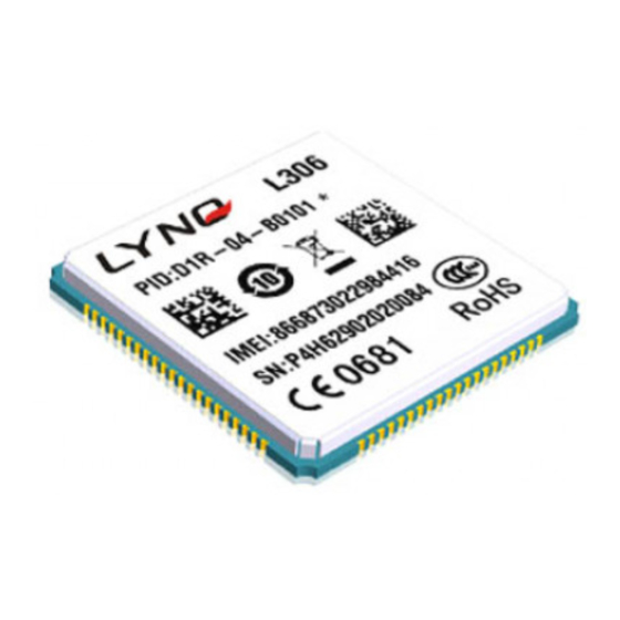
Page 15: Product Labeling
L306 Hardware Design Figure 2-2 Mechanical Dimensions 2.3.2 Product labeling Copyright © Shanghai Mobiletek Communication Ltd... - Page 16 Environment-friendly use period QR code---include IMEI number IMEI number SN number Pin1 mark Module name Module configuration,* stands for E, A or G(refer to table 2-1 and table 2-2) WEEE QR code---include SN number RoHS Copyright © Shanghai Mobiletek Communication Ltd...
-
Page 17: Module Size
L306 Hardware Design 2.3.3 Module size Copyright © Shanghai Mobiletek Communication Ltd... - Page 18 L306 Hardware Design Figure 2-4 Module Size (back view) Copyright © Shanghai Mobiletek Communication Ltd...
-
Page 19: Recommend Pad
L306 Hardware Design 2.3.4 Recommend Pad Copyright © Shanghai Mobiletek Communication Ltd... - Page 20 L306 Hardware Design Figure 2-5 Recommend pad(front view) Copyright © Shanghai Mobiletek Communication Ltd...
-
Page 21: Interface Circuit Design
Notes: According to the environment, please select capacitor as large value as possible; and add 100pF, 33pF capacitors if requiring. Add Zener close to our module. The Zener should be 5.1V/500mW, Ir<100uA @Vr=4.2V. Ta=25℃. Copyright © Shanghai Mobiletek Communication Ltd... -
Page 22: Power Pin Description
PWRKEY is grounded directly. If you do not need to power on the boot, you can control the PWRKEY to achieve. Typical circuit is shown in figure 3-2. Copyright © Shanghai Mobiletek Communication Ltd... -
Page 23: Hardware Reset
Module fourth pin is the hardware reset input. The module will power off when it receives a 20ms low level signal. The system has an internal pull up, the typical value is 1.8V, and do not need to pull up externally. Figure 3-3 System Reset Copyright © Shanghai Mobiletek Communication Ltd... -
Page 24: Usim Interface
USIM_CLK and USIM_DATA signals are recommended to be protected. Between GND and USIM_VCC in parallel with a 1uF and 33pF capacitors, that can filter out the interference of radio frequency signals. Copyright © Shanghai Mobiletek Communication Ltd... -
Page 25: Usb Interface
The differential impedance of differential data lines should be controlled at 90ohm ±10%, and lines should be protected up and down, and can’t be crossed with other lines. USB connection circuit is as follows. Copyright © Shanghai Mobiletek Communication Ltd... -
Page 26: Pcm Interface
DM/DP requires a series 0R resistor. The resistor is placed near the module and the test point is placed between module and resistor. 3.4 PCM Interface PCM application L306 provides a digital audio interface (PCM) that can be used as a PCM master device to transmit Copyright © Shanghai Mobiletek Communication Ltd... -
Page 27: Iic Interface
L306 module does not have a dedicated IIC interface. if you need to use the IIC interface for communication, you should use the GPIO port to simulate the IIC interface, and it is recommended to use an external pull-up resistor of 4.7K by VIO18. Copyright © Shanghai Mobiletek Communication Ltd... -
Page 28: Uart Interface
UART0 receive data input UART0 Ring Indicator. It can be used as UART0_RING wake out signal to host from module UART0_DCD UART0 Data Carrier Detect UART0_TX UART0 transmit data output UART0_DTR Data Terminal Ready(wake up module) Copyright © Shanghai Mobiletek Communication Ltd... -
Page 29: Uart Application
2 wires mode connection. Module interface level is 1.8V. If the AP interface level does not match, you must increase the level conversion circuit. L306 Figure 3-9 Connect to AP method(4lines) L306 Serial Port Serial Port RING RING Figure 3-10 Connect to AP method Copyright © Shanghai Mobiletek Communication Ltd... -
Page 30: Interactive Application Interface
3.8 LED Interface 3.8.1 LED Control circuit GPIO54 (PIN51) can be used to control the network status of the lam; GPIO17 (PIN45) can be used as an indicator of the power supply connected or not. Copyright © Shanghai Mobiletek Communication Ltd... -
Page 31: Led State Description
Table 3-4 LED Status LED Status Module Status Always On Power on Power off GPIO54 is used as the enable pin. Table 3-5 lists the LED status. Table 3-5 LED Status LED Status Module Status Copyright © Shanghai Mobiletek Communication Ltd... - Page 32 L306 Hardware Design Always On Searching Network/Call Connect 300ms ON, 300ms OFF Data Transmit 800ms ON, 800ms OFF Registered network Power off / Sleep Copyright © Shanghai Mobiletek Communication Ltd...
-
Page 33: Electrical Characteristics
Using the DCDC supply, please ensure the capacity of DCDC over 2.0A. We don’t suggest the LDO as the power supplier. 4.2 Temperature characteristic Table 4-2 Temperature characteristic State Min. Nom. Unit Working ℃ Storage ℃ Copyright © Shanghai Mobiletek Communication Ltd... -
Page 34: Absolute Maximum Power
Max. Unit DVDD18 Digital power input for IO Note: All the GPIOs of module are 1.8V. 4.5 Power consumption Table 4-5 Power Consumption Parameter Conditions Min. Average Max. Unit Flight mode Suspend state Standby Copyright © Shanghai Mobiletek Communication Ltd... - Page 35 393 / 490* current WCDMA@CH4408,MAX Power 397 / 490* WCDMA@CH1638,MAX Power / 487* WCDMA@CH9800,MAX Power 450 / 475* WCDMA@CH10700,MAX Power 378 / 482* Peak current Max power mode burst current * Power consumption of L306G. Copyright © Shanghai Mobiletek Communication Ltd...
-
Page 36: Power Sequence
4.7 Digital Interface Characteristics Table 4-6 Digital IO Voltage Parameter Description Min. Typical Max. Unit High level input voltage 1.62 1.98 Low level input voltage High level output voltage 1.62 1.98 Low level output voltage Copyright © Shanghai Mobiletek Communication Ltd... -
Page 37: Esd
3、 USB, UART and other plug connection need to add ESD devices, the other from the outside of the machine out of the control line also need to add ESD devices; 4、 SIM card, users will get inserted t-card touch the place also need to add ESD device; Copyright © Shanghai Mobiletek Communication Ltd... - Page 38 Notes: For ESD protect, please add ESD methods according to upper ways. High speed circuits like USB, TF and SIM card should be added ESD with low capacity value. ESD components include varistors and TVS. For better performance, please use TVS. Copyright © Shanghai Mobiletek Communication Ltd...
-
Page 39: Rf Features
33dBm ± 2dB 5dBm ± 5dB E-GSM900 33dBm ± 2dB 5dBm ± 5dB DCS1800 30dBm ± 2dB 0dBm ± 5dB PCS1900 30dBm ± 2dB 0dBm ± 5dB GSM850(8-PSK) 27dBm ± 3dB 5dBm ± 5dB Copyright © Shanghai Mobiletek Communication Ltd... -
Page 40: Data Link
PCS1900 <-109dBm UMTS2100 <-109dBm UMTS1900 <-109dBm UMTS1732 <-109dBm UMTS850 <-109dBm UMTS900 <-109dBm 5.2 Data link L306 supports GPRS/EDGE CLASS12,and HSDPA/HSDPA R8. The actual application depends on the local network operator. Table 5-4 Data Link Copyright © Shanghai Mobiletek Communication Ltd... -
Page 41: Antenna Design
Polarization refers to the rotation direction of electric field while the antenna is in the direction of maximum radiation. Linear polarization is recommended. It is recommended to use the diversity antenna which has the different polarization direction from the main antenna. Radiation pattern Copyright © Shanghai Mobiletek Communication Ltd... - Page 42 TRP/TIS TRP(Total Radiated Power): GSM850/900 >28dBm GSM1800/1900 >25dBm WCDMA Band1/2/4/5/8 >19dBm TIS(Total Isotropic Sensitivity): GSM850/900/1800/1900 <-102dBm WCDMA Band1/2/4/5/8 <-102dBm Copyright © Shanghai Mobiletek Communication Ltd...
- Page 43 Figure R3, C3, C5 and R5 composition of the antenna matching network for antenna debugging, the default R3, R5 paste 0 ohm resistor C5, C3 empty paste, to be antenna factory after the antenna to determine the value of the antenna. Copyright © Shanghai Mobiletek Communication Ltd...
- Page 44 L306 Hardware Design Note:L306G do not support MIMO Antenna, which main antenna Pad is PIN82. Copyright © Shanghai Mobiletek Communication Ltd...
-
Page 45: Storage And Production
Baking before using, SMT during the time table signs Notes: Moving, storage, production of module must meet the demand of IPC/JEDEC J-STD-033. 6.2 Production The module is a humidity sensitive device. If the device needs reflow soldering, disassembly and Copyright © Shanghai Mobiletek Communication Ltd... -
Page 46: Module Confirmation And Moisture
5. Module is placed naked in the air under 168 hours but not temp 30° C and humidity < 60%. Baking condition confirmation The moisture proof level of the smart module is level 3. And the baking conditions are as follows. Table 6-2 Baking conditions Copyright © Shanghai Mobiletek Communication Ltd... -
Page 47: Smt Reflow Attentions
So, using intelligent modules over the furnace need to pay attention to: Modules can’t be vibrate larger, namely customer requirements as far as possible in orbit (chain) Copyright © Shanghai Mobiletek Communication Ltd... -
Page 48: Smt Stencil Design And The Problem Of Less Tin Soldering
If customer motherboard is thin and slender with a furnace deformation, warping risks, you will be suggested to create "a furnace vehicle" to ensure the welding quality. Other production proposals are as follows: The solder pastes use brands like Alfa. Copyright © Shanghai Mobiletek Communication Ltd... - Page 49 Note: customer’s board deformation must be controlled well. By reducing the number of imposition or increasing patch clamp to reduce the deformation. Module thickness of the stencil is recommended to be thickened, and the rest position can be maintained by 0.1mm. Copyright © Shanghai Mobiletek Communication Ltd...
Need help?
Do you have a question about the LYNO L306 and is the answer not in the manual?
Questions and answers