Pioneer DV-300-S Service Manual
Hide thumbs
Also See for DV-300-S:
- Operating instructions manual (82 pages) ,
- Operating instructions manual (43 pages) ,
- Operating instructions manual (82 pages)
Table of Contents
Advertisement
Quick Links
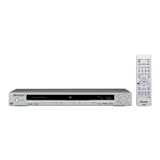
DVD PLAYER
DV-300-S
DV-300-K
THIS MANUAL IS APPLICABLE TO THE FOLLOWING MODEL(S) AND TYPE(S).
Model
Type
DV-300-S
WYXZT5
DV-300-S
WYXZT/UR5
DV-300-K
WYXZT5
DV-300-K
WYXZT/UR5
For details, refer to "
PIONEER CORPORATION
PIONEER ELECTRONICS (USA) INC. P.O. Box 1760, Long Beach, CA 90801-1760, U.S.A.
PIONEER EUROPE NV Haven 1087, Keetberglaan 1, 9120 Melsele, Belgium
PIONEER ELECTRONICS ASIACENTRE PTE. LTD. 253 Alexandra Road, #04-01, Singapore 159936
PIONEER CORPORATION 2007
Power Requirement
AC220-240V
AC220-240V
AC220-240V
AC220-240V
Important Check Points for Good Servicing
4-1, Meguro 1-chome, Meguro-ku, Tokyo 153-8654, Japan
STANDBY/
ON
OPEN/CLOSE
DV-300-S
Region No.
" .
ORDER NO.
TOP MENU
MENU
RRV3561
ENTER
HOME
MENU
RETURN
Remarks
2
5
2
5
T-ZZV FEB. 2007 printed in Japan
Advertisement
Table of Contents

Related Manuals for Pioneer DV-300-S


Summary of Contents for Pioneer DV-300-S
- Page 1 PIONEER CORPORATION 4-1, Meguro 1-chome, Meguro-ku, Tokyo 153-8654, Japan PIONEER ELECTRONICS (USA) INC. P.O. Box 1760, Long Beach, CA 90801-1760, U.S.A. PIONEER EUROPE NV Haven 1087, Keetberglaan 1, 9120 Melsele, Belgium PIONEER ELECTRONICS ASIACENTRE PTE. LTD. 253 Alexandra Road, #04-01, Singapore 159936 PIONEER CORPORATION 2007 T-ZZV FEB.
-
Page 2: Safety Information
2. When the cover is open, close viewing through the objective lens with the naked eye will cause exposure to the laser beam. ∗ : See page 16. /C LO M EN M EN DV-300-S... - Page 3 To protect products from damages or failures during transit, the shipping mode should be set or the shipping screws should be installed before shipment. Please be sure to follow this method especially if it is specified in this manual. DV-300-S...
-
Page 4: Notes On Use
• Soldering time: Within 3 seconds • Soldering combination: Sn-3.0Ag-0.5Cu • When Soldering/Removing of solder, use the draw in equipment over the Pick Up Unit to prevent the Flux smoke from it. Short circuit using a soldering iron. Pick Up PCB Fig. 1 DV-300-S... -
Page 5: Disc Removal Method
• Place the unit on a workstation equipped to protect against static electricity, such as conductive mat. • Soldering iron with ground wire or ceramic type is used. • A worker needs to use a ground conductive wrist strap for body. DV-300-S... -
Page 6: Table Of Contents
9.2 OPERATION 1 PCB and OPERATION 2 PCB ASSYS (WYXZT5 types) ..........67 9.3 OPERATION 1 PCB and OPERATION 2 PCB ASSYS (WYXZT/UR5 types) .......... 68 9.4 POWER PCB ASSY..........................69 10. PCB PARTS LIST ............................71 11. IC .................................. 72 DV-300-S... -
Page 7: Jigs List
Cleaning liquid : GEM1004 Cleaning paper : GED-008 ACCESSORIES Accessories • Audio / Video cable(1.2m) ×1 • Remote control ×1 • Power cable ×1 (red/white/yellow) (07650KY070) (1206158802) (06CPBA2006) • Dry cell batteries ×2 • Warranty Card (AA/R6P) • Operating Instructions DV-300-S... -
Page 8: Block Diagram
1. BLOCK DIAGRAM 1.1 OVERALL BLOCK DIAGRAM DV-300-S... -
Page 9: Dvd Loader Block Diagram
1.2 DVD LOADER BLOCK DIAGRAM DV-300-S... -
Page 10: Power Block Diagram
1.3 POWER BLOCK DIAGRAM DV-300-S... -
Page 11: Diagnosis
DECK DOES NOT ACCEPT OPEN/CLOSE Is the voltage at Check P.CON 6V line of pin 8 and 19 of IC2301 POWER BLOCK. about DC6V ? Check CD2302 Is the lose connection connection to DECK. at CD2302 to DECK ? Change DVD LOADER. DV-300-S... - Page 12 Replace V651 or IC651. NO PLAYBACK PICTURE OF AV JACK Is there Check IC4001 and a signal at pin 164 of peripheral circuit. IC4001 ? Is there Check J7302 and peripheral video signal at pin 33 circuit. of IC7301 ? Change IC7301. DV-300-S...
- Page 13 NO ANALOG AUDIO ON PLAYBACK Is there Check J8003 and peripheral AUDIO signal at pins 1 and 7 circuit. of IC8003 ? Is there Check AT pins 184 and AUDIO signal at C8051 186 of IC4001. and C8053 ? Change IC8003. DV-300-S...
- Page 14 Any kind of symptoms (no power, a failure in any of the servo, video and audio systems, etc.) may be (DVD MT PCB Assy : IC4001) generated, because the DVD processing is performed by a single chip. 64M SDRAM No power. (DVD MT PCB Assy : IC4005) Block noise is generated during playback. DV-300-S...
-
Page 15: Method For Diagnosing Degradation Of The Lds On The Pickup Assy
No playback of a CD : Measure the voltage between the two ends of R2320 or R2322 on the DVDM Assy. If the voltage is 0.4 V or higher, the 780-nm LD is degraded. DVD MT PCB ASSY Front side SIDE A DV-300-S... -
Page 16: Test Mode
• After going into test mode, if you play back the disc, "DISC-NON" is displayed. • The video signal and the audio signal are outputted during the test mode. • The SKIP key and the SCAN key are effective during the test mode. TEST MODE: OFF POWER GGF1381 Test mode remote control unit DV-300-S... -
Page 17: Test Mode In
3 LD ON DVD : Press the [TEST] (A8-5E) and [1] (A8-01) keys in order, and turn on the laser diode (650n). : Press the [TEST] (A8-5E) and [4] (A8-04) keys in order, and turn on the laser diode (780n). DV-300-S... -
Page 18: Display Specification Of The Test Mode
: [NTSC] PAL system : [PAL] Automatic setting : [AUTO] Scart terminal output [SK – ∗ ∗] (Display only the WY model which can do the output setting of scart terminal.) VIDEO : [00] S-VIDEO : [01] : [02] DV-300-S... -
Page 19: Functional Specification Of The Shortcut Key
• Region confirmation mode (ESC + A.MON [Test mode remote control unit] + "1"-"8" [Test mode remote control unit] keys) After you press the A.MON key while holding the ESC key pressed and then input the region number, if the number is different from that set in the unit, an error message is displayed, and the tray opens. DV-300-S... -
Page 20: Functional Specification Of The Service Mode
%%e -2 : NG 7.0e -4 : NG 3 EDC/ID error history (ID Address, EDC/ID errors, last eight errors) Note: ∗ Error of AV1 is not supported in this player. Indication plan contents Character in bold : Item name : Information display DV-300-S... -
Page 21: Disassembly
Up PCB and DVD MT PCB connector. 1-4: DVD MT PCB (Refer to Fig. 1-4) 1. Remove the 3 screws 1. 2. Remove the 4 screws 2. 3. Remove the DVD MT PCB in the direction of arrow. Fig. 1-2 DVD MT PCB Fig. 1-4 DV-300-S... -
Page 22: Dvd Deck Section
Loader Sub Ass'y Gear Pulley Loading Motor Insulator (R) Loading Motor PCB Ass’y Traverse Ass'y • Screw Torque: 2.5 ± 0.3kgf•cm (Screw 1) • Screw Torque: 1.0 ± 0.3kgf•cm (Screw 2) Fig. 2-3-A • Screw Torque: 2.0 ± 0.3kgf•cm Fig. 2-2-A DV-300-S... - Page 23 3 supports 1. between A and B. Fig. 2-3-D 2. Remove the Plate Clamper, Magnet Clamper and Clamper. Check Hook Check Hook Plate Clamper Magnet Clamper Main Frame Loading Motor PCB Ass’y Check Hook Clamper Fig. 2-3-E Fig. 2-5-A DV-300-S...
- Page 24 6. Remove the Switch PCB Ass'y. 7. Remove the screw 4. Feed Motor 8. Remove the Gear Feed. 9. Remove the 2 screws 5. 10. Remove the Feed Motor. Safety surface for pressing 11. Remove the Gear Motor. of the insert. Fig. 2-7-C DV-300-S...
- Page 25 Fig. 2-8. NOTE 1. Do not make the folding lines except the specified positions for the FFC. [ 24 pin FFC ] Fold Printing Surface 79 ± 1 mm Reinforcement Plate To Pick Up PCB Fig. 2-8 DV-300-S...
-
Page 26: Each Setting And Adjustment
While the screen shown at left is being displayed, updating is in progress. DO NOT TURN OFF THE POWER DURING UPDATING. 4 Updating of the firmware is completed. When the screen with the Pioneer logo is displayed, updating is completed. The time required for updating is about 5 minutes. DV-300-S... -
Page 27: Adjustment
2 If updating of the firmware using the disc for updating failed • Was the disc for updating recognized properly? Check if the volume label of the disc is PIONEER. • Is playback of a disc other than the disc for updating possible? If playback of a test CD is also impossible, a reading section, such as PU, may be defective. -
Page 28: Exploded Views And Parts List
For the applying amount of lubricants or glue, follow the instructions in this manual. (In the case of no amount instructions, apply as you think it appropriate.) 6.1 PACKING SECTION WYXZT/UR5 Only WYXZT/UR5 Only WYXZT/UR5 Only WYXZT/UR5 Only DV-300-S... - Page 29 See Contrast table (2) Operating Instructions (S/D) See Contrast table (2) Operating Instructions (R) See Contrast table (2) (2) CONTRAST TABLE DV-300-S/WYXZT5, /WYXZT/UR5, DV-300-K/WYXZT5 and WYXZT/UR5 types are constructed the same except for the following : DV-300-S/ DV-300-S/ DV-300-K/ DV-300-K/ Mark No.
-
Page 30: Exterior Section
6.2 EXTERIOR SECTION NON-CONTACT SIDE CONTACT SIDE DV-300-S... - Page 31 8965TS101B Cord Jumper (CD7301) 122H0C3002 • • • • • • Screw,Tap Tite(S)-Bind Wash. 816423063U (2) CONTRAST TABLE DV-300-S/WYXZT5, /WYXZT/UR5, DV-300-K/WYXZT5 and /WYXZT/UR5 types are constructed the same except for the following : DV-300-S/ DV-3003-S/ DV-300-K/ DV-300-K/ Mark No. Symbol and Description...
-
Page 32: Dvd Mecha Section
Note : (SW PCB ASS'Y) CD2301 NOTE: Applying positions AA, AB and AC for the CLASS PART NO. MARK grease are displayed for this section. GREASE GEM1018 Check if the correct grease is applied for each GYA1001 position. GEM1036 DV-300-S... - Page 33 92P100088A Feed Rack Assy 92AAA0017A Screw,T-Tite(B) (M1.7x5.0 P3) 813381750U Screw,Gear Feed 92P700007A Cord Jumper (CD2301) 122H061605 Switch (SW1) 0515S32003 Push Switch (SW2) 0500101036 Screw,Tap Tite(P) (2.6x8) 811022680U Sems.Tap Tite(P) (2x8) 816112080U Screw (Bind 2x8) 811022080U DVD MECHA ASSY A2K001A650 DV-300-S...
-
Page 34: Specifications
DVD-R/RW compatibility • Compatible formats: DVD-Video, Video Recording (VR)* * Edit points may not play exactly as edited; Super VCD screen may go momentarily blank at edited points. • Unfinalized playback: No • WMA/MP3/JPEG file playback on DVD-R/ RW: No DV-300-S... - Page 35 In these particular instances, check with the software publisher for more detailed information. Discs recorded in packet write mode (UDF format) are not compatible with this player. Check the DVD-R/RW or CD-R/RW software disc boxes for additional compatibility information. DV-300-S...
-
Page 36: Main Specifications
(color): 0.7 Vp-p (75 Ω) (color): 0.7 Vp-p (75 Ω) Jacks ......RCA DV-300-S... -
Page 37: Front Panel Section
Returns to the previously dis-played menu screen. • Press to jump to the previous/next 7 HOME MENU chapter or track. 8 Display Compatible Description of the display. This mark indicates compatibility with DVD-RW discs recorded on a DVD recorder in Video Recording mode. DV-300-S... -
Page 38: Remote Control
Press to pause playback; press again to restart. 12 PLAY MODE Press to display the Play Mode menu. (You can also get to the Play Mode menu by pressing HOME MENU and selecting Play Mode). Press to jump to the beginning of the current DV-300-S... - Page 39 Use to select menu options, etc. playing. 24 ZOOM 18 MENU Press to change the zoom level. Press to display a DVD disc menu, or the Disc Navigator if a VR format DVD-RW, CD, Video CD , MP3, WMA or JPEG disc is loaded. DV-300-S...
-
Page 40: Schematic Diagram
-28V DPF010 ATTENTION CAUTION :LES PIECES REPAREES PAR UN ETANT :SINCE THESE PARTS MARKED BY DANGEREUSES AN POINT DE VUE SECURITE CRITICAL FOR SAFETY,USE ONES N’UTILISER QUE CELLS DECRITES DESCRIBED IN PARTS LIST ONLY DANS LA NOMENCLATURE DES PIECES DV-300-S... - Page 41 LIMIT SW SW(GND) SW(GND) FG SENSER CP2302 DVD PCB PCB130 CLOSE CLOSE DMF089 GND(D) GND(D) OPEN OPEN DVD MECHA ASSY (A2K001A650) NOTE: THIS INTERCONNECTION DIAGRAM IS THE LATEST AT THE TIME OF PRINTING AND SUBJECT TO CHANGE WITHOUT NOTICE DV-300-S...
-
Page 42: Dvd Mt Pcb Assy (1/6)
55 56 57 58 59 60 61 62 63 64 65 66 67 68 69 70 71 72 73 74 75 76 77 78 79 DQ11 DQ12 DQ13 DQ14 DQ15 DBA0 DBA1 MA10 MA11 SDCKE SDCLK 1.8V NOTE:THE DC VOLTAGE EACH PART WAS MEASURED WITH THE DIGITAL TESTER DURING PLAYBACK. DV-300-S... - Page 43 TP4035 TP4092 R4075 R4039 10K RESET TP4093 TP4094 RESET C4118 (V+3D) 100P CH NR4001 4D03WGJ0330T5E B4011 PCB130 MMZ1608R102CT R4076 DMF089 NOTE: T HIS SCHEMATIC DIAGRAM IS THE LATEST AT THE TIME OF PRINTING AND SUBJECT TO CHANGE WITHOUT NOTICE DV-300-S...
-
Page 44: Dvd Mt Pcb Assy(2/6)
0.001 B DQM0 C4040 DCAS# DRAS# DBA1 DBA0 NC (WP#/ACC) SDCLK DCS# RY/BY# PRD# PCE# PRD# PCE# PWR# FROM/TO POWER PORT (V+3D) D_GND NOTE:THIS SCHEMATIC DIAGRAM IS THE LATEST AT THE TIME OF PRINTING AND SUBJECT TO CHANGE WITHOUT NOTICE DV-300-S... - Page 45 DQM0 NC/RFU LDQM DQM1 DWE# UDQM SDCLK DCAS# CAS# SDCKE DRAS# RAS# DCS# MA11 DBA0 BA0/A13 DBA1 BA1/A12 MA10 A10/AP C4055 0.1 B TP4001 NOTE:THE DC VOLTAGE EACH PART WAS PCB130 MEASURED WITH THE DIGITAL TESTER DMF089 DURING PLAYBACK. DV-300-S...
-
Page 46: Dvd Mt Pcb Assy(3/6)
LIMIT SW 3.3K TP2333 TP2325 MOT_SLED- SLD- TP2326 Sled MOT_SLED+ SLD+ R2329 R2310 TP2327 SPD- TP2328 MOT_SPDL+ SPD+ MOT_SPDL- C2307 V+3F 0.1 B W802 C2311 0.1 B NOTE:THE DC VOLTAGE EACH PART WAS MEASURED WITH THE DIGITAL TESTER DURING PLAYBACK. DV-300-S... - Page 47 0.1 B OPIN VOTR- Vcc2 VOTR+ W806 VOLD- VOSL+ C2312 W805 0.1 B VOLD+ VOSL- VOTK- VOFC- VOTK+ VOFC+ NOTE: T HIS SCHEMATIC DIAGRAM IS THE LATEST AT THE TIME PCB130 OF PRINTING AND SUBJECT TO CHANGE WITHOUT NOTICE DMF089 DV-300-S...
-
Page 48: Dvd Mt Pcb Assy(4/6)
NA_P R8048 FROM/TO VIDEO JACK 470K AUDIO_L AUDIO_R V+5V_A NOTE:THIS SCHEMATIC DIAGRAM IS THE LATEST AT THE TIME NOTE:THE DC VOLTAGE EACH PART WAS OF PRINTING AND SUBJECT TO CHANGE WITHOUT NOTICE MEASURED WITH THE DIGITAL TESTER DURING PLAYBACK. DV-300-S... - Page 49 220 +-1% 220 +-1% 12.5 MUTE SW R8076 Q8020 R8061 C8067 C8070 KTC2875-B -1.1 R8077 68P CH AUDIO_R YK_P 220 +-1% R8063 27K +-1% C8072 R8057 0.1 B J8003 RCA-207B-02 AUDIO OUT CAUTION: DIGITAL TRANSISTOR CAUTION: DIGITAL TRANSISTOR PCB130 DMF089 DV-300-S...
-
Page 50: Dvd Mt Pcb Assy(5/6)
: VIDEO SIGNAL ROUTE (B/CB ch) : AUDIO SIGNAL ROUTE (L ch) D_GND NOTE:THE DC VOLTAGE EACH PART WAS NOTE:THIS SCHEMATIC DIAGRAM IS THE LATEST AT THE TIME MEASURED WITH THE DIGITAL TESTER OF PRINTING AND SUBJECT TO CHANGE WITHOUT NOTICE DURING PLAYBACK. DV-300-S... - Page 51 AUDIO R CVBS OUT IC7302 4CH BUS SW SN74CBT3257PWR (GY) (B/CB) (R/CR) (R/CR) YUV only ---> W871,W872,W873,R7306 ON YUV/D ---> W871,W872,W873,W874,W875,W876,R7306 ON RGB/YUV ---> IC7302 MOUNT,JP DEL,R7305 ON J7302 RCA-405A-08 CVBS/Y/U/V CAUTION: DIGITAL TRANSISTOR CAUTION: DIGITAL TRANSISTOR PCB130 DMF089 DV-300-S...
-
Page 52: Dvd Mt Pcb Assy(6/6)
FL DC+ -28V ATTENTION CAUTION :LES PIECES REPAREES PAR UN ETANT :SINCE THESE PARTS MARKED BY DANGEREUSES AN POINT DE VUE SECURITE CRITICAL FOR SAFETY,USE ONES N’UTILISER QUE CELLS DECRITES DESCRIBED IN PARTS LIST ONLY DANS LA NOMENCLATURE DES PIECES DV-300-S... - Page 53 FLDC- FLDC+ -28V D_GND TO MEMORY D_GND NOTE:THIS SCHEMATIC DIAGRAM IS THE LATEST AT THE TIME NOTE:THE DC VOLTAGE EACH PART WAS OF PRINTING AND SUBJECT TO CHANGE WITHOUT NOTICE MEASURED WITH THE DIGITAL TESTER DURING PLAYBACK. PCB130 DMF089 DV-300-S...
-
Page 54: Operation 1 And Operation 2 Pcb Assys (Wyxzt5 Types)
EJECT SW666 EVQ11L05R PCB280 DEF129 Vout OS651 ROM-V340TAO NOTE:THE DC VOLTAGE EACH PART WAS NOTE: THIS SCHEMATIC DIAGRAM IS THE LATEST AT THE TIME MEASURED WITH THE DIGITAL TESTER OF PRINTING AND SUBJECT TO CHANGE WITHOUT NOTICE DURING PLAYBACK. DV-300-S... - Page 55 FP_DI DI (M to F) 100P CH FP_DO DO (F to M) FFC(1.0mm pitch) V+3E R666 V+3E V+3E CD601 C604 2H0B1003 2.2 1/4W DGND C605 33P CH DGND TP663 0.001 B FLDC+ FLDC+ -28V -28V FLDC- FLDC- PCB270 DEF126 DV-300-S...
-
Page 56: Operation 1 And Operation 2 Pcb Assys (Wyxzt/Ur5 Types)
EVQ11L05R EJECT SW666 EVQ11L05R PCB280 DEF129 Vout OS651 ROM-V340TAO NOTE:THE DC VOLTAGE EACH PART WAS NOTE:THIS SCHEMATIC DIAGRAM IS THE LATEST AT THE TIME MEASURED WITH THE DIGITAL TESTER OF PRINTING AND SUBJECT TO CHANGE WITHOUT NOTICE DURING PLAYBACK. DV-300-S... - Page 57 00_6232_011_102_800+ FP_SCK FFC(1.0mm pitch) FP_DI DI (M to F) CD601 FP_DO 2H0B1003 DO (F to M) V+3E R666 V+3E V+3E C604 2.2 1/4W DGND C605 33P CH DGND TP663 0.001 B FLDC+ FLDC+ -28V -28V FLDC- FLDC- PCB270 DEF126 DV-300-S...
-
Page 58: Power Pcb Assy (1/2)
:SINCE THESE PARTS MARKED BY REPLACE ONLY WITH THE SAME TYPE FUSE CRITICAL FOR SAFETY,USE ONES 1.6A 125V{F501} DESCRIBED IN PARTS LIST ONLY ATTENTION :POUR UNE PROTECTION CONTINUE LES RISQUES D’INCEIE N’UTILISER QUE DES FUSIBLE DE MEME TYPE 1.6A 125V{F501} DV-300-S... - Page 59 NOTE:THIS SCHEMATIC DIAGRAM IS THE LATEST AT THE TIME NOTE:THE DC VOLTAGE EACH PART WAS DANGEREUSES AN POINT DE VUE SECURITE OF PRINTING AND SUBJECT TO CHANGE WITHOUT NOTICE MEASURED WITH THE DIGITAL TESTER N’UTILISER QUE CELLS DECRITES DURING PLAYBACK. DANS LA NOMENCLATURE DES PIECES DV-300-S...
-
Page 60: Power Pcb Assy (2/2)
P.CON+D5V MMZ1608R102CT AT+3.3V P.CON+12V P-H/I-L_RGB-H ASP/FS AMP_A_OUT_R AMP_A_OUT_L G/Y_VIDEO B/U_VIDEO R/V_VIDEO CVBS/C_VIDEO A_GND Q8101 Q8102 21PIN CTL IN 12.1 21PIN CTL DRV R8105 KTC3875S_Y_RTK 11.4 KTA1504S_Y_RTK 390 1/4W 11.4 12.1 R8101 4.7K 1/4W CAUTION: DIGITAL TRANSISTOR CAUTION: DIGITAL TRANSISTOR DV-300-S... - Page 61 On that occasion, replace whole Assy. NOTE:THIS SCHEMATIC DIAGRAM IS THE LATEST AT THE TIME NOTE:THE DC VOLTAGE EACH PART WAS PCB240 OF PRINTING AND SUBJECT TO CHANGE WITHOUT NOTICE MEASURED WITH THE DIGITAL TESTER DPF015 DURING PLAYBACK. DV-300-S...
-
Page 62: Wave Forms
IC4001-pin159 (ASPDIF) J7302-pin6 (CVBS_Out) VIDEO JACK V:1.0V/div. H:200nsec/div. V:200mV/div. H:10µsec/div. J8101-pin7 (B/U_Video_Out) V:500mV/div. H:20µsec/div. CP4002-pin1 (FP_SCK) J7302-pin5 (Y_Out) V:1.0V/div. H:20µsec/div. V:500mV/div. H:10µsec/div. J8101-pin15 (R/V_Video_Out) V:500mV/div. H:20µsec/div. AUDIO JACK J7302-pin3 (U_Out) J8003-pin3 (Lch_Out) V:500mV/div. H:20µsec/div. V:1.0V/div. H:500µsec/div. J8101-pin19 (CVBS_Video_Out) V:500mV/div. H:20µsec/div. DV-300-S... - Page 63 Note : The encircled numbers denote measuring point in the schematic diagram. POWER PCB ASSY 21PIN/D-TERMINAL/DIGITAL AUDIO J8101-pin1 (AMP_A_Out_R)) V:1.0V/div. H:200µsec/div. J8101-pin3 (AMP_A_Out_L)) V:1.0V/div. H:200µsec/div. OPERATION 1 PCB ASSY IC651-pin5 (OSC) DISPLAY V:500mV/div. H:1µsec/div. DV-300-S...
-
Page 64: Pcb Connection Diagram
Symbol In PCB Symbol In Schematic Part Name Diagrams Diagrams C E B Capacitor Connector Transistor B C E SIDE A Transistor with resistor B C E Field effect SIDE B P.C.Board Chip Part transistor Resistor array 3-terminal regulator DV-300-S... -
Page 65: Dvd Mt Pcb Assy
W802 R2311 C2317_1 C8067 R2319 R2329 R7317 IC8003 IC2301 Q8020 C8069 R8079 C4096 R2322 R8084 W806 Q8019 IC4006 Q2304 R8057 Q2301 C4094 Q8013 Q2302 Q8018 CP2303 R8085 R8080 C4099 B4002 Q2306 C2301 Q2307 R8083 C4098 C4112 W840 CP4003 CP2301 DV-300-S... - Page 66 SIDE B SIDE B DVD MT PCB ASSY DMF089A R2341 R2343 W834 R4001 W821 R2325 W822 R8060 W833 R8059 R8014 R2308 R8051 W814 R8044 DV-300-S...
-
Page 67: Operation 1 Pcb And Operation 2 Pcb Assys (Wyxzt5 Types)
OPERATION 1 PCB ASSY (INSERTED PARTS) OPERATION 1 PCB ASSY (CHIP MOUNTED PARTS) SW656 SW655 SW652 SW658 W809 SW661 OPERATION 2 PCB ASSY W009 W003 (INSERTED PARTS) W007 D669 W011 W012 W013 W010 OPERATION 2 PCB ASSY (CHIP MOUNTED PARTS) R666 DV-300-S... -
Page 68: Operation 1 Pcb And Operation 2 Pcb Assys (Wyxzt/Ur5 Types)
SIDE A OPERATION 1 PCB ASSY (INSERTED PARTS) OPERATION 1 PCB ASSY (CHIP MOUNTED PARTS) W809 SW658 W007 W009 W003 OPERATION 2 PCB ASSY (INSERTED PARTS) D667 D668 W011 W012 W013 W010 R666 OPERATION 2 PCB ASSY (CHIP MOUNTED PARTS) DV-300-S... -
Page 69: Power Pcb Assy
D510 W001 B502 R534 C526 R8120 C521_1 W025 C522_1 DPF015A C517 R8101 D528 C8112 W037 L8101_1 R539 C519_1 D525 D531 W004 W019 W018 Q504 C520 D523 Q502 R528 C8113 R529 D536 D533 CP502 W035 D535 W011 C528 W016 C8114 DV-300-S... - Page 70 SIDE A SIDE A POWER PCB ASSY (CHIP MOUNTED PARTS) DV-300-S...
-
Page 71: Pcb Parts List
J8001 RCA JACK 060R401122 J8003 RCA JACK 060J451009 X4001 CRYSTAL (27MHz) 100GT02720 OPERATION 1 PCB ASSY SEMICONDUCTORS IC651 IC PT6315 IF4K063150 SWITCHES AND RELAYS SW652 - SW666 SWITCH TACT 0504R01T38 OTHERS V651 TUBE FLUORESCENT 096F82R601 OS651 REMOTE RECEIVER 077A040002 DV-300-S... - Page 72 55 56 57 58 59 60 61 62 63 64 65 66 67 68 69 70 71 72 73 74 75 76 77 78 79 80 81 82 83 84 85 86 87 88 89 90 91 92 93 94 95 96 97 98 99 101 102 103 104 105 106 107 108 DV-300-S...
- Page 73 TV Encoder Module Videop RF Amplifier Video DAC Servo IO Servo Motor Processor Video Drive Processor interlacer Spindle Control FLASH MPEG-1/2 Audio JPEG Memory Video Decoder Controller DRAM System Audio Parser Audio Output CPPM/CPRM SPDIF System GPIO 32-bit RISC IR/VFD DV-300-S...
- Page 74 • Pin Function DV-300-S...
- Page 75 DV-300-S...
- Page 76 DV-300-S...
- Page 77 DV-300-S...
- Page 78 DV-300-S...
- Page 79 DV-300-S...
- Page 80 DV-300-S...
- Page 81 DV-300-S...
- Page 82 DV-300-S...
- Page 83 Note: 1. The Main column is the main function, Alt. means alternative function. 2. The external TV encoder mode only supports CCIR-656 mode. DV-300-S...
Need help?
Do you have a question about the DV-300-S and is the answer not in the manual?
Questions and answers