Table of Contents
Advertisement
Quick Links
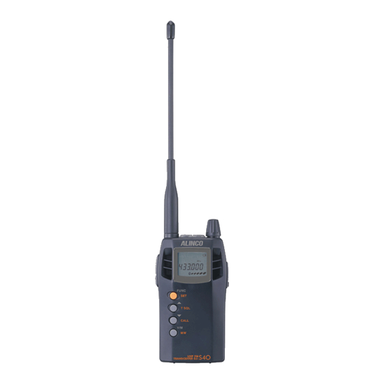
DJ-S40T / E
Service Manual
CONTENTS
1) GENERAL ................................................................ 2
2) TRANSMITTER ........................................................ 2
3) RECEIVER ............................................................... 2
1) Receiver system ....................................................... 3
2) Terminalmitter system ............................................... 4
3) PLL, VCO Circuit ....................................................... 4
4) M38224M6M ............................................................ 5
1) M64082A (XA0543) .................................................. 7
2) NMJ2070MT1 (XA210) ............................................. 8
3) NJM2904V (XA0573) ................................................ 8
4) NJM2902V-TE1 (XA0596) ........................................ 9
5) TA31136FN (XA0404) ............................................... 9
6) UPC2771T (XA0545) .............................................. 10
7) CAT24WC16JITE13 (XA0855) ................................ 10
8) S-816A30AMC (XA0848) ........................................ 10
9) S-80827ALNP (XA0857) ......................................... 11
10) MRF9745T1 (XE0034) ............................................ 11
11) Transistor, Diode and LED Outline Drawings ........... 12
12) LCD Connection ..................................................... 13
All manuals and user guides at all-guides.com
1) Front View ............................................................... 14
2) Bottom View ............................................................ 15
MAIN Unit ......................................................... 16~20
SW Unit .................................................................. 20
Mechanical Parts .................................................... 20
Packing ................................................................... 20
...................................................... 21~22
PC BOARD VIEW
1) UP0433(1/2) side A ................................................ 23
2) UP0433(1/2) side B ................................................ 24
3) PTT Unit WIRING ................................................... 25
............................................. 26
...................................................... 27
ALINCO,INC.
Advertisement
Table of Contents

Related Manuals for Alinco DJ-S40T


Summary of Contents for Alinco DJ-S40T
-
Page 1: Table Of Contents
All manuals and user guides at all-guides.com DJ-S40T / E Service Manual CONTENTS SPECIFICATIONS EXPLODED VIEW 1) GENERAL ..............2 1) Front View ............... 14 2) TRANSMITTER ............2 2) Bottom View ............15 3) RECEIVER ............... 2 PARTS LIST CIRCUIT DESCRIPTION MAIN Unit ............ -
Page 2: Specifications
All manuals and user guides at all-guides.com SPECIFICATIONS 1) GENERAL Frequency coverage T : TX 430 ~ 449.995MHz RX 410 ~ 470MHz E : TX 430 ~ 439.995MHz RX 430 ~ 439.995MHz TA : TX 410 ~ 470MHz RX 410 ~ 470MHz Mode F3E (FM) Channel steps... -
Page 3: Circuit Description
All manuals and user guides at all-guides.com CIRCUIT DESCRIPTION 1) Receiver System The receiver system is a double superheterodyne system with a 21.7MHz first IF and a 450kHz second IF. 1. Front End The signal from the anntena is pssed through low-pass filter and input to RF coil L24 and L17(band pass filter). -
Page 4: Terminalmitter System
All manuals and user guides at all-guides.com 2)Transmitter System 1.Microphone Amplifier The input signal from built-in or external microphone is led to the microphone mute circuit Q15,pre-emphasis circuit ,IDC circuit IC4,the signal is input to the maximum deviation adjustment volume VR2.Then mixed at the add VR2 with the CTCSS tone signal which is generated by CPU,Then it is input to VCO as the modulation signal. -
Page 5: M38224M6M
All manuals and user guides at all-guides.com 4) M38224M6M Terminal Connection (TOP VIEW) - Page 6 All manuals and user guides at all-guides.com Terminal function of CPU No. Pin Name Function I/O Logic Description No. Pin Name Function I/O Logic Description Noise level input for squelch 41 P115 TON3 O Activ high Tone output 3 Key input ( , ,V/M) 42 P14 TON2 O Activ high...
-
Page 7: Semiconductor Data
All manuals and user guides at all-guides.com SEMICONDUCTOR DATA 1) M64082AGP (XA0543) DUAL PLL FREQUENCY SYNTHESIZER Xout CONT Fin1 Fin2 Lock CONT Buffer Xout 1/4 divider Programmable divider 1/2 divider through for reference frequency Data latch (11 or 17 bits) 2-modulus Programmable divider Fin2... -
Page 8: Nmj2070Mt1 (Xa210)
All manuals and user guides at all-guides.com 2) NJM2070MT1 (XA210) Low Voltage Power Amplifier Equivalent Circuit 3) NJM2904V-TE1 (XA0573) -
Page 9: Njm2902V-Te1 (Xa0596)
All manuals and user guides at all-guides.com 4) NJM2902V-TE1 (XA0596) Quad Single Supply Operational Amplifier 5) TA31136FN (XA0404) Low Power FM IF... -
Page 10: Upc2771T(Xa0545)
All manuals and user guides at all-guides.com 6) UPC2771T(XA0545) Terminal Connection (Top View) 1: INPUT 2: GND 3: GND 4: OUTPUT 5: GND 6: Vcc 7) CAT24WC16JITE13 (XA0855) PDIP Name Function User Configurable Chip Selects A0..A2 Ground Serial Address/Data I/O Serial Clock Write Protect Input 2.5V~6.0V Power Supply... -
Page 11: S-80827Alnp (Xa0857)
All manuals and user guides at all-guides.com 9) S-80827ALNP (XA0857) Pin Assignment Top view 1 OUT 3 NC Block Diagram 10) MRF9745T1 (XE0034) PAKEGE DIMENSIONS STYLE 1 : PIN 1. DRAIN 2. GATE 3. SOURCE 4. SOURCE... -
Page 12: Transistor, Diode And Led Outline Drawings
All manuals and user guides at all-guides.com 11) Transistor, Diode and LED Outline Drawings 1SV307(TPH3) 2SA1036K T146Q 2SA1576A 2SB766A-TX 2SC4081 T106R 2SC4618TLP 2SC4808-TX. AR XD0326 XT110 XT0094 XT0170 XT0095 XT0172 XT0171 2SC5066-O(TE85L) 2SD2216R-TX 2SK3074 DA204U HSU277TRF ISV311(TPL3) M1FE 40400V1A XT0138 XT0135 XE0044 XD0130... -
Page 13: Lcd Connection
All manuals and user guides at all-guides.com 12) LCD connection Pin No COM0 COM1 COM2 COM3 COM0 COM1 COM2 COM3... -
Page 14: Exploded View
All manuals and user guides at all-guides.com EXPLODED VIEW 1) Front View UR0023 TN0014 TZ0088 UP0433 TL0027 DG0040 TL0026 EL0053 ST0069 FG0330 KZ0134 YX0032 DP0139... -
Page 15: Bottom View
All manuals and user guides at all-guides.com 2) Bottom View AF0025 AF0031 FG0336 FG0345 RED ( MRCL04AA ) UP0433 BLUE ( MACL04AA ) ES0025 FP0182 TS0165 FG0329 AN0027 FG0333 FG0331 SD0092 NK0077 SD0093 SP0013 FG0346 AN0012 FM0201 RD0108 FG0337 UE0338 FG0332 AX0008 FG0334... -
Page 16: Parts List
All manuals and user guides at all-guides.com PARTS LIST MAIN Unit Version Version Ref. Ref. Parts No. Description Parts Name Parts No. Description Parts Name T E TA T E TA UP0433 PC Board DJS40 INTEGRATED 0.5 0.5 0.5 CS0367 Chip tantalum TMCMA0J106MTR CU3531... - Page 17 All manuals and user guides at all-guides.com Version Version Ref. Ref. Parts No. Description Parts Name Parts No. Description Parts Name T E TA T E TA C128 CU3551 Chip C. GRM36B223K16PT XL0036 Chip Diode SML-310MTT86 C129 CS0367 Chip tantalum TMCMA0J106MTR XL0036 Chip Diode...
- Page 18 All manuals and user guides at all-guides.com Version Version Ref. Ref. Parts No. Description Parts Name Parts No. Description Parts Name T E TA T E TA XT0170 Chip Transistor 2SB766A-TX RK3550 Chip R. ERJ2GEJ103X XT0095 Chip Transistor 2SC4081 T106R RK3564 Chip R.
- Page 19 All manuals and user guides at all-guides.com Version Version Ref. Ref. Parts No. Description Parts Name Parts No. Description Parts Name T E TA T E TA R124 RK3550 Chip R. ERJ2GEJ103X R203 RK3558 Chip R. ERJ2GEJ473X R125 RK3562 Chip R. ERJ2GEJ104X R204 RK3542 Chip R.
-
Page 20: Sw Unit
All manuals and user guides at all-guides.com Mechanical Parts Packing Version Ref. Ref. Version Parts No. Description Parts Name Parts No. Description Parts Name T E TA T E TA MBCL02AA Wire #30B02-20-02 EBP-53N Ni-Cd Bttery Pack MRCL02AA Wire #30R02-20-02 EDC-93 AC Aadaptor(120V) MRCL02AA... -
Page 21: Adjustment
All manuals and user guides at all-guides.com ADJUSTMENT 1. Enter the frequency in memory. (M1 ~ M17) * Refer to Memory Channel’s Frequency List 2. Press FUNC > MONI (Key Lock) > FUNC > > 2 times > V/M > MONI 2 times (It becomes in “Adjustment Mode”... - Page 22 All manuals and user guides at all-guides.com Sta- Adj. or Ter- Adj. Item Frequency (MHz) Adj.Range Condition Check minal Point :435.05 ∼ Rx : 0.8 1.2V :435.05 Check Tx : 1.0 ∼ PD Voltage 1.4V :435.05 :435.05 ± 100Hz Reference :435.05 Adj.
-
Page 23: Up0433(1/2) Side A
All manuals and user guides at all-guides.com PC BO PC BO PC BOARD ARD VIEW VIEW VIEW VIEW PC BO PC BO VIEW 1) 1) 1) 1) 1) UP0433(1/2) Side A UP0433(1/2) Side A UP0433(1/2) Side A UP0433(1/2) Side A UP0433(1/2) Side A... -
Page 24: Up0433(1/2) Side B
All manuals and user guides at all-guides.com 2) 2) 2) 2) 2) UP0433(1/2) Side B UP0433(1/2) Side B UP0433(1/2) Side B UP0433(1/2) Side B UP0433(1/2) Side B... -
Page 25: Ptt Unit Wiring
All manuals and user guides at all-guides.com 3) 3) 3) 3) 3) PTT Unit PTT Unit PTT Unit PTT Unit PTT Unit WIRING WIRING WIRING WIRING WIRING... -
Page 26: Schematic Diagram
All manuals and user guides at all-guides.com SCHEMA SCHEMA SCHEMA SCHEMA SCHEMATIC DIA TIC DIA TIC DIA TIC DIA TIC DIAGRAM GRAM GRAM GRAM GRAM... -
Page 27: Block Diagram
All manuals and user guides at all-guides.com BLOCK DIA BLOCK DIA BLOCK DIA BLOCK DIA BLOCK DIAGRAM GRAM GRAM GRAM GRAM TX:410-470MHz RX:430-449.995MHz (T) TX/RX:430-439.995MHz (E) - Page 28 All manuals and user guides at all-guides.com...
- Page 29 All manuals and user guides at all-guides.com...
- Page 30 DJ-195 DJ-195 DJ-195 DJ-195 vice Man vice Man Ser vice Man vice Man vice Man ual ALINCO ALINCO , , , , , INC. ALINCO INC. INC. ALINCO ALINCO INC. INC. Head Office : Head Office : Head Office : Shin-Dai Building 9th Floor...
Need help?
Do you have a question about the DJ-S40T and is the answer not in the manual?
Questions and answers