Table of Contents
Advertisement
Quick Links
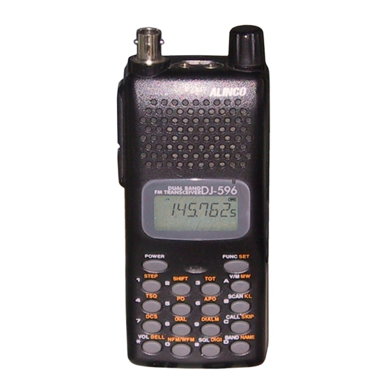
DJ-596T / DJ-596E
Service Manual
CONTENTS
1) GENERAL ................................................................ 2
2) TRANSMITTER ........................................................ 2
3) RECEIVER ............................................................... 2
1) [RX] ...................................................................... 3~5
2) [TX] ........................................................................... 5
3) M38267M8L(XA0844) ........................................... 6~8
1) µPC2710T (XA0449) ................................................ 9
2) S-81350HG-KD-T1 (XA0724) ................................... 9
3) 24LC32AT-I/SN (XA0604) ....................................... 10
4) M5222FP-600C (XA0385) ...................................... 10
5) TC4W53FU (XA0348) ............................................. 11
6) TK10931V (XA0666) ............................................... 11
7) NJM2902V-TE1 (XA0596) ...................................... 12
8) NJM2070M (XA0210) ............................................. 12
9) µPD3140GS-E1 (XA0312) ...................................... 13
10) BA4510FV-E2 (XA0537) ......................................... 14
11) S-80845ALMP-EA9-T2 (XA0620) ........................... 14
12) MB88347LPFV-G-BND-EF (XA0599) ..................... 15
13) Transistor, Diode and LED Outline Drawings ........... 16
14) LCD Connection(EL0044) ....................................... 16
1) Front View ............................................................... 17
2) Rear View ............................................................... 18
MAIN Unit ......................................................... 19~24
Mechanical Parts .................................................... 24
Packing ................................................................... 24
1) Required Test Equipment .................................. 25~26
.................................................. 33~34
...................................................... 36
............................................. 35
ALINCO,INC.
Advertisement
Table of Contents

Related Manuals for Alinco DJ-596T


Summary of Contents for Alinco DJ-596T
-
Page 1: Table Of Contents
DJ-596T / DJ-596E Service Manual CONTENTS SPECIFICATIONS EXPLODED VIEW 1) GENERAL ..............2 1) Front View ............... 17 2) TRANSMITTER ............2 2) Rear View ............... 18 3) RECEIVER ............... 2 PARTS LIST CIRCUIT DESCRIPTION MAIN Unit ............19~24 1) [RX] ..............3~5 Mechanical Parts ............ -
Page 2: Specifications
SPECIFICATIONS General Type D J-596T DJ-596E 136.000-173.995MHz 144.000-145.995MHz Receiving Range 400.000-511.995MHz 430.000-439.995MHz 144.000-147.995MHz 144.000-145.995MHz Transmitter Range 420.000-449.995MHz 430.000-439.995MHz Modulation F2, F3 +14˚ F~+ 140˚ F ) Frequency Stability ± 5ppm -10˚C~+60˚C Ant.Impedance 50Ω Supply Voltage 6.0~16.0VDC DC13.8V VHF Approx.1.2A UHF : Approx.1.4A Transmit 9.6V EBP-50N Approx.1.2A, UHF Approx.1.5A... -
Page 3: Circuit Description
CIRCUIT DESCRIPTION 1) [RX] 1. RX Method: Double Super Heterodyne Method 1st IF FM 39.15 MHz 2nd IF 2. Front End The signal input from antenna passes through the duplexer FL1 and low pass filter, then it is amplified at RF amplifier Q17. The amplified signal is led to band pass filter and band switch D19, then input to the mixer Q16. - Page 4 5. Squelch Q24 determines the gain of AF signal output from pin 12 of IC5 according to the WFM/NFM of IC8. Then the signal is input to pin 19 of IC5. The input signal passes through the noise filter amplifier and rectifier circuit, then output from pin 21 of IC5.
- Page 5 IC2 compares the frequency gained by dividing the signal added to pin 19 of IC2 by the control signal from IC6 with the frequency gained by dividing the reference frequency of 12.9 MHz inside IC2. When the phase difference is found as a result of phase comparison, the pulse signal is output from the charge pump output of pin 13 of IC2, then the signal is converted into the DC voltage at the inside circuit for passive filter and added to the cathode side of...
-
Page 6: M38267M8L(Xa0844)
3) M38267M8L (XA0844) Terminal Connection (TOP VIEW) - Page 7 Terminal Signal Description P67/AN7 S-meter input P66/AN6 Noise level input for squelch P65/AN5 Low battery detection input P64/AN4 CTCSS/DCS tone input P63/SCLK22/AN3 Band plan 1 P62/SCLK21/AN2 DCS signal mute P61/SOUT2/AN1 DCSW DCS signal mute P60/SIN2/AN0 FKEY Function key input P57/ADT/DA2 CTCSS/DCS tone output, Tuning voltage output P56/DA1 DTOUT...
- Page 8 Terminal Signal Description P15/SEG39 Key matrix output P14/ SEG38 Key matrix output P13/ SEG37 UHF-PLL power ON/OFF output P12/ SEG36 VHF-PLL power ON/OFF output P11/ SEG35 UHF-TX power ON/OFF output P10/ SEG34 AF AMP power ON/OFF output P07/SEG33 VHF-TX power ON/OFF output P06/SEG32 RX power ON/OFF output P05/SEG31...
-
Page 9: Semiconductor Data
SEMICONDUCTOR DATA 1) µ µ µ µ µ PC2710T (XA0449) RF Amplifier Parameter Symbol Condition Ratings Unit Supply voltage Circuit current Vcc=5V, no signa Power gain Vcc=5V, f=500MHz Staturated output power Po(sat) Vcc=5V, f=500MHz, Pin=-8dBm +13.5 Noise figure Vcc=5V, f=500MHz Upper frequency (-3dB) Vcc=5V, Reference freq. -
Page 10: 24Lc32At-I/Sn (Xa0604)
3) 24LC32AT-I/SN (XA0604) 32K 2.5V I C Serial EEPROM PDIP Name Function A0..A2 User Configurable Chip Selects Ground Serial Address/Data I/O Serial Clock Write Protect Input +2.5V~6.0V Power Supply 4) M5222FP-600C (XA0385) Electronic Volume... -
Page 11: Tc4W53Fu (Xa0348)
5) TC4W53FU (XA0348) 6) TK10931V (XA0666) Pin Assignment / BLOCK Diagram (Top View) RECT FM DET RSSI MIXER... -
Page 12: Njm2902V-Te1 (Xa0596)
7) NJM2902V-TE1 (XA0596) Quad Single Supply Operational Amplifier 8) NJM2070M (XA0210) -
Page 13: Μpd3140Gs-E1 (Xa0312)
9) µ µ µ µ µ PD3140GS-E1 (XA0312) 80 ~ 550MHz Dual PLL Synthesizer Specifications Operating frequency: 200 ~ 400MHz (Vin=-12 ~ 0dBm, pin 2 and 19 input) 80 ~ 550MHz (Vin=-8 ~ 0dBm, pin 2 and 19 input) Consumption current: 2.7 ~ 4.1mA (Vcc=1.8V while 1 channel is used) 4.3 ~ 6.6mA (Vcc=1.8V while both channels are used) 0 ~ 10uA (Vcc=1.8V in power save mode) -
Page 14: Ba4510Fv-E2 (Xa0537)
10) BA4510FV-E2 (XA0537) Dual Operational Amplifier Vcc=± 2.5V Typ High through rate: 5V/µSec Block Diagram (Top View) 11) S-80845ALMP-EA9-T2 (XA0620) Voltage Regulator... -
Page 15: Mb88347Lpfv-G-Bnd-Ef (Xa0599)
12) MB88347LPFV-G-BND-EF (XA0599) D/A converter for digital tuning... -
Page 16: Transistor, Diode And Led Outline Drawings
13) Transistor, Diode, and LED Ontline Drawings Top View 1SV214 TPH4 1SV279 (TPH3) 1SV307(TPH3) 1SV311 TPL3 2SB766A-TX 2SD2216R-TX 2SC5066FT-Y(TE85L) XD0131 XD0364 XD0326 XD0344 XT0170 XT0180 XT0135 2SK882-GR-TE85L 2SK2975-T11-A 2SK3074 BRPG1201W TR DA204U T106 DAN235E-TL ISS390 TE61 XE0040 XE0038 XE0044 XL0028 XD0130 XD0320 XD0342... -
Page 17: Exploded View
EXPLODED VIEW 1) Front View... -
Page 18: Rear View
2) Rear View... -
Page 19: Parts List
PARTS LIST MAIN Unit Description Part Name Description Part Name Parts No. Parts No. Ref. No. Ref. No. RADIATIVE PLATE Chip C. GRM36B471K50PT FM0194 CU3531 Chip C. GRM36B103K16PT FG0291 CU3547 LCD RUBBER CONNECT Chip C. GRM36B102K50PT TL0022 CU3535 REFLECTIVE SHEET 195 SILICON DUMPER TMCP0J225MTR TZ0049... - Page 20 Description Part Name Description Part Name Parts No. Parts No. Ref. No. Ref. No. C107 Chip C. C173 Chip C. CU3519 GRM36CH470J50PT CU3111 C1608JB1C104KT-N C108 Chip C. C174 Chip C. GRM36B332K50PT CU3512 GRM36CH120J50PT CU3541 C109 Chip C. GRM36B103K16PT C175 Chip C. GRM36B223K16PT CU3551 CU3547...
- Page 21 Description Part Name Description Part Name Parts No. Parts No. Ref. No. Ref. No. C235 M38267M8L275GP CS0408 Chip Tantalum 6MCM156MATER XA0844 C236 Chip C. 24LC32AT-I/SN CU3018 C1608CH1H390JT-AS XA0604 C237 Chip C. NJM2902V-TE1 XA0596 CU3512 GRM36CH120J50PT NJM2070M T1 C238 Chip C. CU3515 GRM36CH220J50PT XA0210...
- Page 22 Description Part Name Description Part Name Parts No. Parts No. Ref. No. Ref. No. Chip R. ERJ2GEJ823X XP1501-TX RK3561 XU0172 Chip Transistor Chip R. ERJ2GEJ332X RK3544 XP1501-TX XU0172 Chip Transistor Chip R. ERJ2GEJ682X RK3548 XT0180 Chip Transistor 2SC5066FT-Y (TE85L) Chip R. ERJ2GEJ472X XP1501-TX RK3546...
- Page 23 Description Part Name Description Part Name Parts No. Parts No. Ref. No. Ref. No. Chip R. ERJ2GEJ122X R146 Chip R. ERJ2GEJ103X RK3550 RK3539 R147 Chip R. ERJ2GEJ102X Chip R. ERJ2GEJ122X RK3538 RK3539 R148 Chip R. ERJ2GEJ103X Chip R. ERJ2GEJ104X RK3562 RK3550 Chip R.
-
Page 24: Mechanical Parts
Mechanical Parts Description Part Name Parts No. Ref. No. R210 Chip R. ERJ2GEJ104X RK3562 R211 Chip R. ERJ2GEJ473X RK3558 Description Part Name Parts No. Ref. No. R212 Chip R. ERJ2GEJ473X RK3558 CHASSIS DJ596 SS0097 R213 Chip R. ERJ2GEJ331X RK3532 KL6767-PTT DJ195 FG0290 R214 Chip R. -
Page 25: Adjustment
ADJUSTMENT 1) Required Test Equipment The following items are required to adjust radio parameters. 1. Regulated Power supply Supply voltage: 5 to14 VDC Current: 3A or more 2. Digital Multimeter Voltage range: FS = Approx. 20V Current: 10A or more Input resistance: High impedance 3. - Page 26 11.Frequency Counter Measurable frequency: Up to 500MHz Measurable stability: Approx. ± 0.1ppm 12.Linear Detector Measurable frequency: Up to 500MHz Characteristics: Flat 60 dB or more Note · Standard modulation: 1kHz ± 3.5kHz /DEV · Reference sensitivity: 12dB SINAD · Specified audio output level: 200mW at 8Ω ·...
-
Page 27: Entering And Releasing The Adjustment Mode
2) Entering and releasing the adjustment mode The DJ-596 does not require a serviceperson to manipulate the components on the printed-circuit board, except the trimmer when adjusting reference frequency and deviation. Most of the adjustments for the transceiver are made by using the keys on it while the unit is in the adjustment mode. - Page 28 Reference frequency adjustment 1. In the adjustment mode, select channel 1 by rotating the main tuning dial. 2. Press the key to start transmission. 3. Rotate TC1 on the main board until the value on the frequency counter matches the one displayed on the LCD. UHF high-power adjustment 1.
- Page 29 VHF minimum frequency sensitivity adjustment See “Note on adjusting the sensitivity” later in this section. 1. In the adjustment mode, select channel 6 by rotating the main tuning dial. 2. Set the minimum frequency sensitivity rotating the main tuning dial, while F appears after the key is pressed.
- Page 30 VHF S-meter (FULL) adjustment 1. In the adjustment mode, select channel 13 by rotating the main tuning dial. The S-meter will show all circles ( 2. Enter “+20” dBµ (EMF) with the transceiver tester (SSG). 3. Press the key. The transceiver beeps indicating the new setting has been stored successfully.
- Page 31 UHF narrow deviation adjustment 1. In the adjustment mode, select channel 19 by rotating the main tuning dial. 2. Input a 50mVrms, 1kHz signal with your transceiver tester through the external microphone jack. 3. With the tester, put the transceiver in the transmission mode. 4.
- Page 32 Tone 88.5Hz test 1. In the adjustment mode, select channel 23 by rotating the main tuning dial. 2. Press the key. An 88.5Hz tone is automatically sent. 3. Check the deviation with the transceiver tester, and make sure the deviation level is within 0.4 to 1.2kHz range.
-
Page 33: Pc Board View
PC BOARD VIEW MAIN SIDE A... - Page 34 MAIN SIDE B...
- Page 37 DJ-195 Service Manual ALINCO, INC. Head Office : Shin-Dai Building 9th Floor 2-6, 1-Chome, Dojimahama, Kita-ku, Osaka 530-0004, Japan Phone: +81-6-4797-2136 Fax: +81-6-4797-2157 E-mail:export@alinco.co.jp Dealer/Distributor Copyright 2001 Alinco, lnc. Osaka Japan Printed in Japan PM0071...
Need help?
Do you have a question about the DJ-596T and is the answer not in the manual?
Questions and answers