Alinco DR-135 Service Manual
Hide thumbs
Also See for DR-135:
- Service manual (71 pages) ,
- Dealer's manual (20 pages) ,
- Service manual (60 pages)
Table of Contents
Advertisement
Quick Links
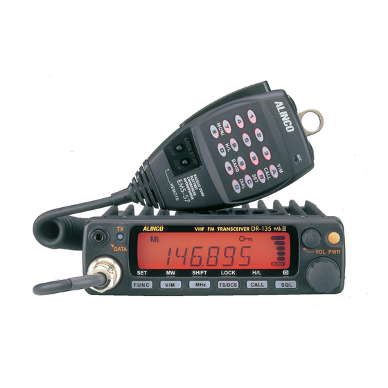
DR-135 / DR-235 / DR-435
Service Manual
CONTENTS
GENERAL ........................................................................................ 2
TRANSMITTER ................................................................................ 2
RECEIVER ....................................................................................... 2
CIRCUIT DESCRIPTION DR-135
1) Receiver System (DR-135) ........................................................... 3, 4
2) Transmitter System (DR-135) ....................................................... 4, 5
3) PLL Synthesizer Circuit (DR-135) ................................................. 5, 6
4) Receiver System (DR-235) ........................................................... 6, 7
5) Transmitter System (DR-235) ....................................................... 7, 8
6) PLL Synthesizer Circuit (DR-235) ................................................. 8, 9
7) Receiver System (DR-435) ......................................................... 9, 10
8) Transmitter System (DR-435) ......................................................... 10
9) PLL Synthesizer Circuit (DR-435) ................................................... 11
10) CPU and Peripheral Circuits(DR-135 DR-235 DR-435) ............. 11,12
11) Power Supply Circuit ....................................................................... 13
12) M3826M8269GP (XA0818) ....................................................... 14~16
1) M5218FP (XA0068) ........................................................................ 17
2) NJM7808FA (XA0102) .................................................................... 17
3) TC4S66F (XA0115) ........................................................................ 17
4) TK10930VTL (XA0223) .................................................................. 18
5) BU4052BF (XA0236) ...................................................................... 19
6) TC4W53FU (XA0348) .................................................................... 19
7) M64076GP (XA0352) ..................................................................... 20
8) LA4425A (XA0410) ......................................................................... 21
9) M67746 (XA0412) .......................................................................... 21
10) M68729 (XA0591) .......................................................................... 22
11) M57788 (XA0077A) ........................................................................ 23
12) mPC2710T (XA0449) ..................................................................... 24
13) NJM2902 (XA0596) ........................................................................ 24
14) 24LC32A (XA0604) ........................................................................ 25
15) S-80845ALMP-EA9-T2 (XA0620) ................................................... 25
16) L88MS05TLL (XA0675) .................................................................. 25
17) AN8010M (XA0119) ....................................................................... 26
18) TK10489M (XA0314) ...................................................................... 26
19) Transistor, Diode, and LED Ontline Drawings .................................. 27
20) LCD Connection (TTR3626UPFDHN) ........................................... 28
1) Top and Front View ......................................................................... 29
2) Bottom View .................................................................................... 30
3) LCD Assembly ................................................................................ 31
CPU .......................................................................................... 32, 33
Main Unit(DR-135) .................................................................... 33~36
Main Unit(DR-235) .................................................................... 36~39
VCO Unit(DR-235) ......................................................................... 39
Main Unit(DR-435) .......................................................................... 42
VCO Unit(DR-435) ......................................................................... 42
All manuals and user guides at all-guides.com
Mechanical Parts ............................................................................ 43
Packing Parts ................................................................................. 43
ACCESSORIES .............................................................................. 43
ACCESSORIES(SCREW SET) ...................................................... 43
TNC(EJ41U) .................................................................................. 44
TNC (EJ41U) Packing Parts ........................................................... 45
1) Adjustment Spot ............................................................................ 46
2) VCO and RX Adjustment Specification ........................................... 47
3) Tx Adjustment Specification ............................................................ 47
4) Rx Test Specification ....................................................................... 48
5) Tx Test Specification ....................................................................... 49
1) Adjustment Spot ............................................................................ 50
2) VCO and RX Adjustment Specification ........................................... 51
3) Tx Adjustment Specification ............................................................ 51
4) Rx Test Specification ....................................................................... 52
5) Tx Test Specification ....................................................................... 53
1) Adjustment Spot ............................................................................ 54
2) VCO and RX Adjustment Specification ........................................... 55
3) Tx Adjustment Specification ............................................................ 55
4) Rx Test Specification ....................................................................... 56
5) Tx Test Specification ....................................................................... 57
1) CPU Unit Side A ............................................................................. 58
2) CPU Unit Side B ............................................................................. 58
3) Main Unit Side A DR-135 (UP 0400B) ............................................. 59
4) Main Unit Side B DR-135 (UP 0400B) ............................................. 59
5) Main Unit Side A DR-235 (UP 0414) ............................................... 60
6) Main Unit Side B DR-235 (UP 0414) ............................................... 60
7) Main Unit Side A DR-435 (UP 0415) ............................................... 61
8) Main Unit Side B DR-435 (UP 0415) ............................................... 61
9) Tnc Unit Side A (UP 0402) (DR-135TP only) .................................. 62
10) Tnc Unit Side B (UP 0402) (DR-135TP only) .................................. 62
1) CPU Unit DR-135 / DR-235 / DR-435 ............................................. 63
2) Main Unit DR-135 ........................................................................... 64
3) Main Unit DR-235 ........................................................................... 65
4) Main Unit DR-435 ........................................................................... 66
5) TNC Unit (DR-135TP only) ............................................................. 67
1) DR-135 ........................................................................................... 68
2) DR-235 ........................................................................................... 69
3) DR-435 ........................................................................................... 70
Advertisement
Table of Contents

Related Manuals for Alinco DR-135


Summary of Contents for Alinco DR-135
-
Page 1: Table Of Contents
10) M68729 (XA0591) ................22 2) CPU Unit Side B ................58 11) M57788 (XA0077A) ................ 23 3) Main Unit Side A DR-135 (UP 0400B) ..........59 12) mPC2710T (XA0449) ..............24 4) Main Unit Side B DR-135 (UP 0400B) ..........59 13) NJM2902 (XA0596) ................ -
Page 2: Specifications
All manuals and user guides at all-guides.com SPECIFICATIONS General Frequency coverage DR-135 DR-235 DR-435 118.000 ~ 135.995MHz (AM RX) 216.000 ~ 279.995MHz (RX) 350.000 ~ 511.995MHz (RX) T,TG 136.000 ~ 173.995MHz (RX) 222.000 ~ 224.995MHz (TX) 430.000 ~ 449.995MHz (TX) (U.S amateur) -
Page 3: Circuit Description
All manuals and user guides at all-guides.com CIRCUIT DESCRIPTION DR-135/DR-235/DR-435 1) Receiver System (DR-135) The receiver system is a double superheterodyne system with a 21.7 MHz first IF and a 450 kHz second IF . 1. Front End The received signal at any frequency in the 136.000MHz to 173.995MHz range... -
Page 4: Transmitter System (Dr-135)
The 2nd IF 450 kHz signal which passes through filter FL101 (wide) and FL102 (narrow) during narrow, changes its width using the width control switching IC103 and IC102. 2) Transmitter System (DR-135) 1. Modulator Circuit The audio signal is converted to an electrical signal by the microphone, and input it to the microphone amplifier (Q6). -
Page 5: Pll Synthesizer Circuit (Dr-135)
(Q118, Q117, Q116), then it controls the APC voltage supplied to the younger amplifier Q115 and the final power module IC110 to fix the transmission power. 3) PLL Synthesizer Circuit (DR-135) 1. PLL The dividing ratio is obtained by sending data from the CPU (IC1) to pin 2 and sending clock pulses to pin 3 of the PLL IC (IC116). -
Page 6: Receiver System (Dr-235)
All manuals and user guides at all-guides.com 5. VCO Circuit A Colpitts oscillation circuit driven by Q131 directly oscillates the desired frequency. The frequency control voltage determined in the CPU (IC1) and PLL circuit is input to the varicaps (D122 and D123). This change the oscillation frequency, which is amplified by the VCO buffer (Q134) and output from the VCO area. -
Page 7: Transmitter System (Dr-235)
All manuals and user guides at all-guides.com 4. Audio Circuit The audio signal from pin 12 of IC108 is amplified by the audio amplifier (IC104:A), and switched by the signal switch IC (IC111) and then input it to the de-emphasis circuit. and is compensated to the audio frequency characteristics in the de-emphasis circuit (R203, R207, R213, R209, C191, C218, C217) and amplified by the AF amplifier (IC104:D). -
Page 8: Pll Synthesizer Circuit (Dr-235)
All manuals and user guides at all-guides.com 2. Power Amplifier Circuit The transmitted signal is oscillated by the VCO, amplified by the drive amplifier (IC112) and younger amplifier (Q115), and input to the final power module (IC110). The signal is then amplified by the final power module (IC110) and led to the antenna switch (D110) and low-pass filter (L113, L114, L115, L116, C215, C216, C202, C203 and C204), where unwanted high harmonic waves are reduced as needed, and the resulting signal is supplied to the antenna. -
Page 9: Receiver System (Dr-435)
All manuals and user guides at all-guides.com 5. VCO Circuit A Colpitts oscillation circuit driven by Q503 directly oscillates the desired frequency. The frequency control voltage determined in the CPU (IC1) and PLL circuit is input to the varicaps (D503 and D504). This change the oscillation frequency, which is amplified by the VCO buffer (Q504) and output from the VCO area. -
Page 10: Transmitter System (Dr-435)
All manuals and user guides at all-guides.com 5. Squelch Circuit The detected output which is outputted from the pin 11 of IC108 is inputted to pin 13 of IC108 after it was been amplified by IC104:A and it is outputted from pin 14 after the noise component was been eliminated from the composed band pass filter in the built in amplifier of the IC, then the signal is rectified by D106 to convert into DC component. -
Page 11: Pll Synthesizer Circuit (Dr-435)
(D502 and D503). This change the oscillation frequency, which is amplified by the VCO buffer (Q503,504) and output from the VCO unit. 10) CPU and Peripheral Circuits (DR-135 DR-235 DR-435) 1. LCD Display Circuit The CPU turns ON the LCD via segment and common terminals with 1/4 the... - Page 12 All manuals and user guides at all-guides.com 2. Dimmer Circuit The dimmer circuit makes the output of pin 13 of CPU (IC1) into "H" level at set mode, so that Q9 and Q3 will turn ON to make the lamp control resistor R84 short and make its illumination bright.
-
Page 13: Power Supply Circuit
All manuals and user guides at all-guides.com 11) Power Supply Circuit When power supply is ON, there is a "L" signal being inputted to pin 39 (PSW) of CPU which enables the CPU to work. Then, "H" signal is outputted from the pin 41 (C5C) of CPU and drives ON the power supply switch control Q8 and Q7 which turns the 5VS ON. -
Page 14: M3826M8269Gp (Xa0818)
All manuals and user guides at all-guides.com 12) M3826M8L269GP (XA0818) Terminal Connection (TOP VIEW) - Page 15 All manuals and user guides at all-guides.com Pin Name Function I/O PU Logic Description P67/AN7 S-meter input P66/AN6 Noise level input for squelch P65/AN5 Battery voltage input P64/AN4 CTCSS tone input/DSC code input 5 P63/SCLK22/AN3 Band plan 1 6 P62/SCLK21/AN2 Band plan 2 7 P61/SOUT2/AN1 DCSW Activ high...
- Page 16 All manuals and user guides at all-guides.com Pin Name Function I/O PU Logic Description P06/SEG32 P05/SEG31 P04/SEG30 P03/SEG29 P02/SEG28 P01/SEG27 P00/SEG26 P37/SEG25 P36/SEG24 P35/SEG23 P34/SEG22 P33/SEG21 P32/SEG20 P31/SEG19 P30/SEG18 SEG17 SEG16 LCD segment signal SEG15 SEG14 SEG13 SEG12 SEG11 SEG10 SEG9 SEG8 SEG7...
-
Page 17: Semiconductor Data
All manuals and user guides at all-guides.com SEMICONDUCTOR DATA 1) M5218FP (XA0068) Dual Low Noise Operational Amplifiers Output 1 Power Supply Plus Inverting Input 1 Output 2 Non Inverting Input 1 Inverting Input 2 Power supply Minus Non Inverting Input 2 2) NJM7808FA (XA0102) Pin Assignment 1. -
Page 18: Tk10930Vtl (Xa0223)
All manuals and user guides at all-guides.com 4) TK10930VTL (XA0223) Narrow Band FM IF IC IF IN 10.7MHz AF OUTPUT (AM) 4.7K 270K S DET AM DET FM DET IF AMP FM AF OUT AF OUTPUT (FM) 8.2K CFU455D Vcc 3V Parameter Symbol Ratings... -
Page 19: Bu4052Bf (Xa0236)
All manuals and user guides at all-guides.com 5) BU4052BF (XA0236) Analog Multiplexer/Demultiplexer 6) TC4W53FU (XA0348) Multiplexer/Demultiplexer Function Table COMMON Control input ON channel NONE * Don't Care... -
Page 20: M64076Gp (Xa0352)
All manuals and user guides at all-guides.com 7) M64076GP (XA0352) Dual PLL Synthesizer Parameter Symbol Condition Min. Typ. Max. Unit Fin=80~520MHz Power supply voltage Vin=-10dBm LPF supply voltage Fin=80~520MHz Local oscillator input level Vin=-20~-4dBm Local oscillator input frequency Vcc=2.7~5.5V Vcc=2.7~5.5V Vcc=2.7~5.5V Vp-p Xin input level... -
Page 21: La4425A (Xa0410)
All manuals and user guides at all-guides.com 8) LA4425A (XA0410) 5W Audio Power Amplifiers Test Circuit 13.2V LA4425 2.2 F Input 1000 F Vcc=13.2V RL=4 Po =5W Gain= 45dB 9) M67746 (XA0412) 144 ~ 148MHz 60W RF Power Module Rating Symbol Ratings Unit... -
Page 22: M68729 (Xa0591)
All manuals and user guides at all-guides.com 10) M68729 (XA0591) 220 ~ 246MHz 30W RF Power Module ABSOLUTE MAXIMUM RATING(TC = 25˚C) Rating Symbol Ratings Unit Supply voltage M68729 Total current Input power Pin(max) Output Power Po(max) Operation case temperature Tc(op) -30 to + 110 Strage temperature... -
Page 23: M57788 (Xa0077A)
All manuals and user guides at all-guides.com 11) M57788M (XA0077) -
Page 24: Mpc2710T (Xa0449)
All manuals and user guides at all-guides.com 12) µ µ µ µ µ PC2710T (XA0449) RF Amplifier Parameter Symbol Condition Ratings Unit Supply voltage Circuit current Vcc=5V, no signa Power gain Vcc=5V, f=500MHz Staturated output power Po(sat) Vcc=5V, f=500MHz, Pin=-8dBm +13.5 Noise figure Vcc=5V, f=500MHz... -
Page 25: 24Lc32A (Xa0604)
All manuals and user guides at all-guides.com 14) 24LC32A (XA0604) PDIP Name Function A0..A2 User Configurable Chip Selects Ground Serial Address/Data I/O Serial Clock Write Protect Input 2.5V~6.0V Power Supply 15) S-80845ALMP-EA9-T2 (XA0620) 16) L88MS05TLL (XA0675) 5V Voltage Regulator With On/Off Function Pin Assignment 1. -
Page 26: An8010M (Xa0119)
All manuals and user guides at all-guides.com 17) AN8010M (XA0119) Voltage Regulator Test Circuit Vout AN8010M Output Common Input AN8010M 18) TK10489M (XA0314) SQUELCH S DET QUAD DET... -
Page 27: Transistor, Diode, And Led Ontline Drawings
All manuals and user guides at all-guides.com 19) Transistor, Diode, and LED Outline Drawings Top View 1SV214 1SV237 1SV262 1SV268 RLS-73 1SS356 1SS355 XD0131 XD0141 XD0300 XD0301 XD0363 XD0254 XD0272 DA204U DAN235U DSA3A1 MA304 MA729 MA8100 MA742 XD0130 XD0246 XD0131 XD0299 XD0300 XD0297... -
Page 28: Lcd Connection (Ttr3626Upfdhn)
All manuals and user guides at all-guides.com 20) LCD Connection (TTR3626UPFDHN) -
Page 29: Exploded View
All manuals and user guides at all-guides.com EXPLODED VIEW 1) Top and Front View AA0050 AV0006 FG0273 DR-135 : DP0127 DR-235 : DP0135 DR-435 : DP0136 AV0006 T. E. TA NK0072 KZ0105 TG. EG. TAG NK0073 KZ0120... -
Page 30: Bottom View
AA0050 T. E. TA KS0068 TG. EG. TAG KS0070 AV0006 UA0037Y AV0006 AV0006 UX1047 AW0001 ST0065 AZ0042 AE0029 FG0320 UE0401 ES0017 (DR-135 / 435 only) AV0006 ST0066 TG0034 UE0258 FF0015 UX1251 YZ0131 T. E. TA SS0093 TG. EG. TAG SS0095... -
Page 31: Lcd Assembly
All manuals and user guides at all-guides.com 3) LCD Assembly CPU BOARD FM0034 NUT (UE0035) FG0305 FF0017 ST0068 TL0023 DG0037 TL0024 EL0049 ST0064... -
Page 32: Parts List
All manuals and user guides at all-guides.com PARTS LIST Ref. Ref. Parts No. Description Parts Name Parts No. Description Parts Name DR-135 DR-235 DR-435 DR-135 DR-235 DR-435 CU3111 Chip C. C1608JB1C104KT-N RK3046 Chip R. MCR03EZHJ472 CU3111 Chip C. C1608JB1C104KT-N RK3001 Chip R. -
Page 33: Main Unit
All manuals and user guides at all-guides.com Ref. Ref. Parts No. Description Parts Name Parts No. Description Parts Name DR-135 DR-235 DR-435 DR-135 DR-235 DR-435 UU0015Z Switch EVQPPXA25 C173 CU3037 Chip C. C1608JB1H152KT-AS CU3029 Chip C. C1608JB1H331KT-AS UU0015Z Switch EVQPPXA25... - Page 34 All manuals and user guides at all-guides.com Ref. Ref. Parts No. Description Parts Name Parts No. Description Parts Name DR-135 DR-235 DR-435 DR-135 DR-235 DR-435 XD0254 Chip Diode 1SS355 TE17 C263 CE0100 Electrolytic C. 16MV 22UW D117 XD0130 Chip Diode...
- Page 35 All manuals and user guides at all-guides.com Ref. Ref. Parts No. Description Parts Name Parts No. Description Parts Name DR-135 DR-235 DR-435 DR-135 DR-235 DR-435 XU0131 Chip Transistor DTC114EUA T106 R189 RK3038 Chip R. MCR03EZHJ102 Q133 XT0124 Chip Transistor 2SC4215-Y(TE85L)
-
Page 36: Main Unit
All manuals and user guides at all-guides.com Ref. Ref. Parts No. Description Parts Name Parts No. Description Parts Name DR-135 DR-235 DR-435 DR-135 DR-235 DR-435 R279 RK3046 Chip R. MCR03EZHJ472 C109 CS0216 Chip tantalum TMCMB1A106MTR R280 RK3058 Chip R. MCR03EZHJ473... - Page 37 All manuals and user guides at all-guides.com Ref. Ref. Parts No. Description Parts Name Parts No. Description Parts Name DR-135 DR-235 DR-435 DR-135 DR-235 DR-435 C211 CU3003 Chip C. C1608CH1H020CT-AS CN102 UE0397 Connector 10-5082-3110-17-100 C212 CE0364 Electrolytic C. 16MV 47SWB+TS...
- Page 38 All manuals and user guides at all-guides.com Ref. Ref. Parts No. Description Parts Name Parts No. Description Parts Name DR-135 DR-235 DR-435 DR-135 DR-235 DR-435 Q128 XU0131 Chip Transistor DTC114EUA T106 R193 RK3043 Chip R. MCR03EZHJ272 Q129 XU0148 Chip Transistor DTC144EUA T106...
-
Page 39: Vco Unit(Dr-235)
All manuals and user guides at all-guides.com Ref. Ref. Parts No. Description Parts Name Parts No. Description Parts Name DR-135 DR-235 DR-435 DR-135 DR-235 DR-435 R295 RK3038 Chip R. MCR03EZHJ102 L505 QC0104 Chip Inductor LER015T1R5M R297 RK3050 Chip R. MCR03EZHJ103... - Page 40 All manuals and user guides at all-guides.com Ref. Ref. Parts No. Description Parts Name Parts No. Description Parts Name DR-135 DR-235 DR-435 DR-135 DR-235 DR-435 C167 CU3035 Chip C. C1608JB1H102KT-AS C286 CU3027 Chip C. C1608CH1H221JT-AS C169 CU3035 Chip C. C1608JB1H102KT-AS...
- Page 41 All manuals and user guides at all-guides.com Ref. Ref. Parts No. Description Parts Name Parts No. Description Parts Name DR-135 DR-235 DR-435 DR-135 DR-235 DR-435 L118 QKA95D Coil MR3.0 9.5T 0.6 R153 RK3038 Chip R. MCR03EZHJ102 L119 QC0059 Chip Inductor...
-
Page 42: Vco Unit(Dr-435)
All manuals and user guides at all-guides.com Ref. Ref. Parts No. Description Parts Name Parts No. Description Parts Name DR-135 DR-235 DR-435 DR-135 DR-235 DR-435 R259 RK3050 Chip R. MCR03EZHJ103 C513 CS0063 Chip tantalum TMCSA1V104MTR R260 RK3054 Chip R. MCR03EZHJ223... -
Page 43: Packing Parts
All manuals and user guides at all-guides.com Ref. Parts No. Description Parts Name DR-135 DR-235 DR-435 ST0065 SP Holder DR135 ST0066 SP FITTING DR135 TG0034 SP Himelon DR135 UE0258 ANT Connector FM-M.D.R-(4) YZ0131 Tape #9110 12X1mm DS0388A Model Name Plate... -
Page 44: Tnc(Ej41U)
All manuals and user guides at all-guides.com TNC (EJ41U) Ref.No. Parts No. Description Parts Name Ref.No. Parts No. Description Parts Name BAT1 ED0006 Battery BR2032 1F2 RK3038 Chip R. MCR03EZHJ102 CS0408 Chip Tantal 6MCM156MATER RK3038 Chip R. MCR03EZHJ102 CS0408 Chip Tantal 6MCM156MATER RK3038 Chip R. -
Page 45: Tnc (Ej41U) Packing Parts
All manuals and user guides at all-guides.com TNC (EJ41U) Packing Parts Ref.No. Parts No. Description Parts Name FD0001 Floppy-Disc (WIN2HD) FF0034 VELCRO FG0040 Cushion HK0487 Package Item Carton EJ41U HP0029 Plastic bag 5X100X100 HP0040 Plastic bag 8X130X200 PF0061 SHEET EJ41U PR0449 Label EJ41U... -
Page 46: Adjustment
All manuals and user guides at all-guides.com DR-135 ADJUSTMENT 1) Adjustment Spot Power Supply Voltage 13.8 V Output of SSG is all EMF indication If without instruction, WIDE mode If without instruction, SSG output is MOD 1KHz WIDE DEV 3.5KHz/DEV, NARROW DEV 1.75KHz/DEV Standard Modulation is also based above. -
Page 47: Vco And Rx Adjustment Specification
All manuals and user guides at all-guides.com 2) VCO and RX Adjustment Specification ITEM UNIT ADJ.SPOT ADJUSTING METHOD CONDITION Adjustment 145.90MHz MAIN TC101 Adjust so that Tx Frequency Frequency becomes within 145.90MHz±100Hz 136.00MHz MAIN L123 Adjust so that PD voltage becomes Adjustment 1.5V 173.99MHz... -
Page 48: Rx Test Specification
All manuals and user guides at all-guides.com 4) Rx Test Specification TEST ITEM CONDITION ADJ STANDARD TEST STANDARD NOTE RX Sensitivity 136.05MHz Less than -7dBu Less than -6dBu 12dBSINAD 146.05MHz Less than -8dBu Less than -7dBu 173.95MHz Less than -6dBu Less than -5dBu 146.05MHz Less than -8dBu... -
Page 49: Tx Test Specification
All manuals and user guides at all-guides.com 5) Tx Test Specification TEST ITEM CONDITION ADJ STANDARD TEST STANDARD NOTE TX Output 136.00MHz TA,TAG ONLY More than More than HI POWER 144.00MHz 50±3W 146.00MHz 50±1W 50±3W 148.00MHz 50±3W T,TG ONLY 173.99MHz More than More than TA,TAG ONLY... -
Page 50: Adjustment
All manuals and user guides at all-guides.com DR-235 ADJUSTMENT 1) Adjustment Spot Power Supply Voltage 13.8 V Output of SSG is all EMF indication If without instruction, WIDE mode If without instruction, SSG output is MOD 1KHz WIDE DEV 3.5KHz/DEV, NARROW DEV 1.75KHz/DEV Standard Modulation is also based above. -
Page 51: Vco And Rx Adjustment Specification
All manuals and user guides at all-guides.com 2) VCO and RX Adjustment Specification ITEM CONDITION UNIT ADJ.SPOT ADJUSTING METHOD Adjustment 224.90MHz MAIN TC101 Adjust so that Tx Frequency Frequency becomes within 224.90MHz±100Hz 225.00MHz L503 Adjust so that PD voltage becomes Adjustment 2.2V 224.99MHz... -
Page 52: Rx Test Specification
All manuals and user guides at all-guides.com 4) Rx Test Specification TEST ITEM CONDITION ADJ STANDARD TEST STANDARD NOTE RX Sensitivity 216.05MHz Less than -7dBu Less than -6dBu 12dBSINAD 223.50MHz Less than -8dBu Less than -7dBu 250.05MHz Less than -3dBu Less than -2dBu 223.50MHz Less than -8dBu... -
Page 53: Tx Test Specification
All manuals and user guides at all-guides.com 5) Tx Test Specification TEST ITEM CONDITION ADJ STANDARD TEST STANDARD NOTE TX Output 222.00MHz 25±1W 25±3W HI POWER 223.50MHz 25±1W 25±3W 224.99MHz 25±1W 25±3W TX Output 223.50MHz 10±1W 10±2W MID POWER TX Output 223.50MHz 4.5±1W 3~6W... -
Page 54: Adjustment
All manuals and user guides at all-guides.com DR-435 ADJUSTMENT 1) Adjustment Spot Power Supply Voltage 13.8 V Output of SSG is all EMF indication If without instruction, WIDE mode If without instruction, SSG output is MOD 1KHz WIDE DEV 3.5KHz/DEV, NARROW DEV 1.75KHz/DEV Standard Modulation is also based above. -
Page 55: Vco And Rx Adjustment Specification
All manuals and user guides at all-guides.com 2) VCO and RX Adjustment Specification ITEM CONDITION UNIT ADJ.SPOT ADJUSTING METHOD Adjustment 439.00MHz MAIN TC101 Adjust so that Tx Frequency Frequency becomes within 439.00MHz±100Hz 425.00MHz L503 Adjust so that PD voltage becomes Adjustment 1.7V 511.95MHz... -
Page 56: Rx Test Specification
All manuals and user guides at all-guides.com 4) Rx Test Specification TEST ITEM CONDITION ADJ STANDARD TEST STANDARD NOTE RX Sensitivity 350.05MHz Less than -1dBu Less than 0dBu 12dBSINAD 430.05MHz Less than -7.5dBu Less than-6.5dBu 440.05MHz Less than-7.5dBu Less than-6.5dBu 450.05MHz Less than-7.5dBu Less than-6.5dBu... -
Page 57: Tx Test Specification
All manuals and user guides at all-guides.com 5) Tx Test Specification TEST ITEM CONDITION ADJ STANDARD TEST STANDARD NOTE TX Output 430.00MHz 35±3W HI POWER 440.00MHz 35±1W 35±3W 450.00MHz 35±3W T,TG ONLY TX Output 440.00MHz 10±1W 10±2W MID POWER TX Output 440.00MHz 5±1W 5±2W... -
Page 58: Pc Board View
All manuals and user guides at all-guides.com PC BOARD VIEW 1) CPU Unit Side A DR-135 (UP 0400B) DR-235 (UP 0414) DR-435 (UP 0415) 2) CPU Unit Side B DR-135 (UP 0400B) DR-235 (UP 0414) DR-435 (UP 0415) DR135 T, TG... -
Page 59: Main Unit Side A Dr-135 (Up 0400B)
All manuals and user guides at all-guides.com 3) MAIN Unit Side A DR-135 (UP 0400B) 4) MAIN Unit Side B DR-135 (UP 0400B) -
Page 60: Main Unit Side A Dr-235 (Up 0414)
All manuals and user guides at all-guides.com 5) MAIN Unit Side A DR-235 (UP 0414) 6) MAIN Unit Side B DR-235 (UP 0414) -
Page 61: Main Unit Side A Dr-435 (Up 0415)
All manuals and user guides at all-guides.com 7) MAIN Unit Side A DR-435 (UP 0415) 8) MAIN Unit Side B DR-435 (UP 0415) -
Page 62: Tnc Unit Side A (Up 0402) (Dr-135Tp Only)
All manuals and user guides at all-guides.com 9) TNC Unit Side A (UP 0402) (DR-135TP only) 10) TNC Unit Side B (UP 0402) (DR-135TP only) OPTION unit (EJ41U) -
Page 63: Schematic Diagram 1) Cpu Unit Dr-135 / Dr-235 / Dr-435
All manuals and user guides at all-guides.com SCHMATIC DIAGRAM 1) CPU Unit DR-135 / DR-235 / DR-435 TO MAIN CN102 TO MAIN CN103 DR135 T, TG JUMPER DR135 E, EG JUMPER DR135 TA, TAG DR235 T, TG JUMPER DR435 T, TG... -
Page 64: Main Unit Dr-135
All manuals and user guides at all-guides.com 2) MAIN Unit DR-135 5.0V 12.2V 1.1V 600mVp-p 50mVp-p 600mVp-p 300mVp-p TO OPTION 4.9V 4.9V 300mVp-p 300mVp-p 1.9V 300mVp-p TO CPU 300mVp-p 4.5V 7.6V TO CPU OPTION 7.8V 500mVp-p 3.2V 0.6V RX IN : 1KHz 3.5KHz/DEV 60dBu... -
Page 65: Main Unit Dr-235
All manuals and user guides at all-guides.com 3) MAIN Unit DR-235 TO OPTION TO CPU TO CPU OPTION... -
Page 66: Main Unit Dr-435
All manuals and user guides at all-guides.com 4) MAIN Unit DR-435 TO OPTION TO CPU TO CPU OPTION RX IN : 1KHz 3.5KHz/DEV 60dBu TX IN : 1KHz 4mVemf Hi Power... -
Page 67: Tnc Unit (Dr-135Tp Only)
All manuals and user guides at all-guides.com 5) TNC Unit (DR-135TP only) or option TO MAIN CN107... -
Page 68: Block Diagram
All manuals and user guides at all-guides.com BLOCK DIAGRAM... - Page 69 All manuals and user guides at all-guides.com...
- Page 70 All manuals and user guides at all-guides.com...
-
Page 71: Alinco,Inc
U.S.A. : 438 Amapola Ave., Suite 130, Torrance, CA 90501-6201, U.S.A. Phone: 310-618-8616 Fax: 310-618-8758 http://www.alinco.com/ Germany : Eschborner Landstrasse 55, 60489 Frankfurt am Main, Germany Phone: 069-786018 Fax: 069-789-60766 http://www.alinco.de/ Dealer/Distributor Copyright 2000 Alinco, lnc. Osaka Japan Printed in Japan PM0063...
Need help?
Do you have a question about the DR-135 and is the answer not in the manual?
Questions and answers