Samsung HT-D4500 Service Manual
Hide thumbs
Also See for HT-D4500:
- User manual (287 pages) ,
- Firmware upgrade manual (1 page) ,
- User manual (71 pages)
Table of Contents
Advertisement
Quick Links
SERVICE
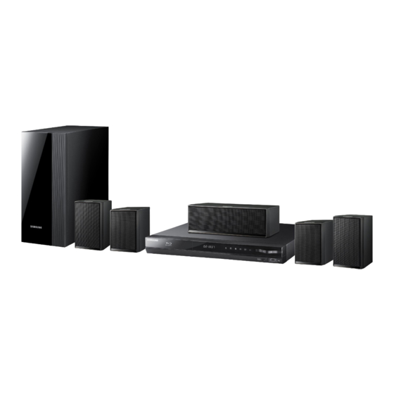
Home Entertainment System
HT-D4500
Refer to the service manual in the GSPN (see the rear cover) for more information.
Home Entertainment
System
Model Name
Model Code
MANUAL
1. Precaution
2. Product Specification
3. Disassembly & Reassembly
4. Troubleshooting
5. PCB Diagram
6. Schematic Diagram
HT-D4500
HT-D4500/EN
Contents
Advertisement
Table of Contents

Related Manuals for Samsung HT-D4500


Summary of Contents for Samsung HT-D4500
- Page 1 Home Entertainment System Model Name HT-D4500 Model Code HT-D4500/EN SERVICE MANUAL Home Entertainment System Contents 1. Precaution 2. Product Specification 3. Disassembly & Reassembly 4. Troubleshooting 5. PCB Diagram HT-D4500 6. Schematic Diagram Refer to the service manual in the GSPN (see the rear cover) for more information.
-
Page 2: Table Of Contents
PCB Diagram ........................... 5 − 1 5.1. Wiring Diagram........................5 − 1 5.2. FRONT PCB Top ........................5 − 2 5.2.1. Pin Connection ......................5 − 3 5.2.2. Test Point Wave Form ....................5 − 4 Copyright© 1995-2011 SAMSUNG. All rights reserved. - Page 3 6.14. FLASH MEMORY/EMMC MOVINAND..................6 − 17 6.15. FIRENCE POWER JTAG DEBUG ..................... 6 − 18 6.16. FRONT-END BLOCK......................6 − 19 6.17. FIR END RAPTOR........................6 − 20 6.18. SMPS ............................ 6 − 21 Copyright© 1995-2011 SAMSUNG. All rights reserved.
-
Page 4: Precaution
TES T ALL EXPO S ED METAL SU RFACES 2-WIRE CORD ALSO TES T WITH PLUG REVER S ED (US ING AC EARTH ADAPTER P LUG GROUND AS R EQ UIRED) Figure 1.1 AC Leakage Test Copyright© 1995-2011 SAMSUNG. All rights reserved. - Page 5 A replacement part that does not have the same safety characteristics as the original might create shock, fire or other hazards. Copyright© 1995-2011 SAMSUNG. All rights reserved.
-
Page 6: Servicing Precautions
CAUTION First read the “Safety Precautions” section of this manual. If some unforeseen circumstance creates a conflict between the servicing and safety precautions, always follow the safety precautions. Copyright© 1995-2011 SAMSUNG. All rights reserved. -
Page 7: Precautions For Electrostatically Sensitive Devices (Esds)
8) Minimize body motions when handling unpackaged replacement ESDs. Motions such as brushing clothes together, or lifting a foot from a carpeted floor can generate enough static electricity to damage an ESD. Copyright© 1995-2011 SAMSUNG. All rights reserved. -
Page 8: Product Specification
Download in Standby Mode • Remote iPod / iPhone support (Digital USB Audio) • Network Feature Search All Your Video • Remote Hot Key Netflix, Smart Hub, Search All • BD Remote Control • One Foot Connection Copyright© 1995-2011 SAMSUNG. All rights reserved. -
Page 9: Specifications
165W x 2(3Ω) Surround speaker output Subwoofer speaker output 170W(3Ω) Amplifier Analog input : 20Hz~20kHz (±3dB) • Frequency response Digital input : 20Hz~40kHz (±-4dB) • 70dB S/N Ratio Channel separation 60dB Input sensitivity (AUX)500mV Copyright© 1995-2011 SAMSUNG. All rights reserved. - Page 10 Center : 8.97 x 3.03 x 2.75 inches (W x H x D) Subwoofer : 6.61 x 13.78 x 11.22 inches Front : 0.94 Ibs Surround : 0.73 Ibs Weights Center : 1.06 Ibs Subwoofer : 8.38 Ibs Copyright© 1995-2011 SAMSUNG. All rights reserved.
-
Page 11: Ht-D4200 Specifications
Front speaker output 165W x 2(3Ω) 170W(3Ω) Subwoofer speaker output Analog input : 20Hz~20kHz (±3dB) • Frequency response Digital input : 20Hz~40kHz (±-4dB) • Amplifier S/N Ratio 70dB 60dB Channel separation Input sensitivity (AUX)500mV Copyright© 1995-2011 SAMSUNG. All rights reserved. - Page 12 Maximum input 330W 340W Front : 90 x 139 x 70 mm Dimensions (W x H x D) Subwoofer : 168 x 350 x 285 mm Front : 0.42 kg Weights Subwoofer : 3.62 kg Copyright© 1995-2011 SAMSUNG. All rights reserved.
-
Page 13: Specifications Analysis
HDMI IN X / X / X X / 2 inputs / 2 inputs 2 inputs One Board (S-ATA) One Board (S-ATA) One Board (S-ATA) Main ↔ Loader O: Feature Included, X: Not Included Copyright© 1995-2011 SAMSUNG. All rights reserved. -
Page 14: Accessories
2. Product Specification 2.4. Accessories 2.4.1. Supplied Accessories Accessories Item Item code Remark Remote Control AH59-02345A Batteries (AAA size) 4301-000116 Video Cable AH39-40001V Local Samsung Dealer FM Antenna AH42-00021A User’s Manual AH68-02406M Copyright© 1995-2011 SAMSUNG. All rights reserved. -
Page 15: Disassembly & Reassembly
2. Unfasten 2 screws on the side for Top Cover. : BH, +, B, M3, L10, ZPC (BLK), SWRCH18A 5. Unfasten 3 screws and 2 holder for taking out VFD Cover. : BH, +, B, M3, L10, ZPC (BLK), SWRCH18A Copyright© 1995-2011 SAMSUNG. All rights reserved. - Page 16 11. Then, only the Bottom Chassis is left. 8. For Main Assy, unfasten 3 screws on the rear side. (Tuner, SPK Jack, AV Jack) : BH, +, B, M3, L10, ZPC (BLK), SWRCH18A Copyright© 1995-2011 SAMSUNG. All rights reserved.
-
Page 17: Troubleshooting
4. Troubleshooting 4. Troubleshooting 4.1. Checkpoints by Error Mode Oscilloscope Setting Values Normal Voltage 24MHz 32.768KHz Voltage/DIV 2V/div 0.5V/div 0.5V/div TIME/DIV 100ms/div 10ns/div 5us/div Copyright© 1995-2011 SAMSUNG. All rights reserved. -
Page 18: No Power
Ye s Che ck co mp one nts a round IC. Re place compone nt RA805, DA805, RA807, if it ha s proble m. RA809. Ye s Re pla ce SMPS ASS ’Y. Copyright© 1995-2011 SAMSUNG. All rights reserved. - Page 19 Check TRA802 ICA1 pin 7 14~19V • → Check TRA801/802 • → Check OCM801 • → Check MA801, TA801S, DRA821/822 • •ICA1 1V < pin 2 < 4.2V → Check for shortage Replace ICA1 Copyright© 1995-2011 SAMSUNG. All rights reserved.
-
Page 20: No Sound
R1026 ~ R1 031 S igna l OK? Cha nge MAIN P CB. Ye s L2001 ~ L2006 S igna l OK? Cha nge AMP P CB. Ye s Check the signal from jack and if not, change AMP. Copyright© 1995-2011 SAMSUNG. All rights reserved. -
Page 21: Disc Loading Error
Is th e De ck c a ble (be twe e n MAIN & DECK) Re ins e rt DECK ca ble corre ctly. inse rte d co rre ctly? Ye s Cha nge the DECK. Copyright© 1995-2011 SAMSUNG. All rights reserved. -
Page 22: Remote Doesn't Work
REM_EYE Pin 1 S igna l OK? Re fe r to wa ve pa ttern Ye s ima ge of Fig. 4-1 . Cha nge the powe r of IC23 Pin 7, ch a nge the MAIN P CB. Copyright© 1995-2011 SAMSUNG. All rights reserved. - Page 23 FC 2 FC 2 50 V 50 V 100UF 100UF 47N F 47N F REMOC ON REMOC ON DGND DGND * 6.2. FRONT <HDMI EYE S IGNAL> * 5.2. FRONT P CB Top <Fig. 4-1> Copyright© 1995-2011 SAMSUNG. All rights reserved.
-
Page 24: No Logo (Hdmi) - Label A
Ye s Change MAIN PCB or System MICOM. Check IC29 ’s crystal signal is OK? Re fer to w a ve pa tter n Ye s ima ge of Fig. 4-3 . HDMI Cable Error. Copyright© 1995-2011 SAMSUNG. All rights reserved. - Page 25 RCLAMP 0524P .TCT RCLAMP 0524P .TCT H_T0+ H_T0+ AL5V_PW AL5V_PW H_T0- H_T0- H_TC+ H_TC+ H_TC- H_TC- * 6.11. HDMI MICOM <HDMI EYE S IGNAL> IC29 N 9 5 * 5.4. MAIN P CB Top <Fig. 4-2> Copyright© 1995-2011 SAMSUNG. All rights reserved.
- Page 26 HDMITX_TX2N HDMITX_TX2N HDMITX_TX1P HDMITX_TX1P HDMITX_TX1N HDMITX_TX1N HDMITX_TX0P HDMITX_TX0P * 6.11. HDMI MICOM <X52 Mus t be 24MHz> IC1 3 IC29 CN95 IC1 7 CN 1 * 5.4. MAIN P CB Top <Fig. 4-3> 4-10 Copyright© 1995-2011 SAMSUNG. All rights reserved.
-
Page 27: No Logo (Component) - Label B
Vide o output from IC11 s olde ring a nd de vice s . * Refe r to wave pa tte rn Ye s ima ge of Fig. 4-5 . Compone nt Ca ble Error. Copyright© 1995-2011 SAMSUNG. All rights reserved. 4-11... - Page 28 * 6.6. AUDIO/VIDEO/IP OD OUT CEC * 5.5. MAIN P CB Bottom C121 C122 C123 <C121 Y S igna l> <C122 P b S igna l> <C123 P r S igna l> <Fig. 4-4> 4-12 Copyright© 1995-2011 SAMSUNG. All rights reserved.
- Page 29 * 6.6. AUDIO/VIDEO/IP OD OUT CEC IC41 IC13 IC29 * 5.4. MAIN P CB Top R181 R182 R183 <R181 Y S igna l> <R182 P b S igna l> <R183 P r S igna l> <Fig. 4-5> Copyright© 1995-2011 SAMSUNG. All rights reserved. 4-13...
-
Page 30: No Logo (Composite)
Vide o output from IC11 P in14 . proble m, cha nge the MAIN P CB. * Refe r to wave pa tte rn Ye s ima ge of Fig. 4-7 . Compone nt Ca ble Error. 4-14 Copyright© 1995-2011 SAMSUNG. All rights reserved. - Page 31 R161 R161 10KOHM 10KOHM 1/16W 1/16W * 6.6. AUDIO/VIDEO/IP OD OUT CEC C847 <C847 Compos it Color Ba r> IC13 IC29 CN95 IC17 CN 1 * 5.4. MAIN P CB Top <Fig. 4-6> Copyright© 1995-2011 SAMSUNG. All rights reserved. 4-15...
- Page 32 SD/ HD_OUT3 DGND DGND * 6.6. AUDIO/VIDEO/IP OD OUT CEC R820 <C820 Compos it Color Ba r> IC 1 3 IC 2 9 IC 1 7 * 5.4. MAIN P CB Top <Fig. 4-7> 4-16 Copyright© 1995-2011 SAMSUNG. All rights reserved.
-
Page 33: Disc Skips Or Freezing
BD: ove r 400mV Cha nge the DECK. DVD: ove r 200mV CD: ove r 200mV Ye s Ye s On ly CD NG? Cha nge the MAIN BOARD. Cha nge the MAIN BOARD. Copyright© 1995-2011 SAMSUNG. All rights reserved. 4-17... -
Page 34: No Disc Reading Error
Consuit with the Samsung Electronics. which is a va ila ble on the Sa m- sung We b Site Ye s Update with the new version and try a ga in. 4-18 Copyright© 1995-2011 SAMSUNG. All rights reserved. -
Page 35: Network Error
The connection between LAN and SET is direct. So there is no need to check H/W if there is network problem. If it is, the problem is MAIN CHIP (IC1)'s BGA soldering problem. It must be changed to a new board. Copyright© 1995-2011 SAMSUNG. All rights reserved. 4-19... -
Page 36: Initialization & Upgrade Methods
Step 2: press and hold INFO button on the remote over 5 seconds. Then, you will see the screen below • Method 2 Select the Settings on the menu. Settings→ Support→ Software Upgrade or Contact Samsung • Description for the meaning Front : System micom S/W : BACKEND Firmware... -
Page 37: How To Update Firmware
The upgrade is complete when the product turns off, and then turns on again by itself. Never turn the product off or back on manually during the update process. Samsung Electronics shall take no legal responsibility for product malfunction caused by an unstable Internet connection or consumer negligence during a software upgrade. - Page 38 8) Select By Disc. NOTE When the system upgrade is done, check the software details in the software Upgrade menu. Do not turn off the product during the Software Upgrade. It may cause the product malfunction. 4-22 Copyright© 1995-2011 SAMSUNG. All rights reserved.
-
Page 39: Cold Start Method (Initialize Setup)
3) Then, VFD sign : “Initialize” → Power will be turned off automatically. 4) System Micom Cold Start : During Stand-By, just press the Stop Button “■” for over 5 seconds. Then, the power LED will glitter. Copyright© 1995-2011 SAMSUNG. All rights reserved. 4-23... -
Page 40: Buyer-Region Code Setting Method
NOTE The “T-MODE” indicator on the VFD only appears for a very short time. 3) You can see “TEST − −” on the VFD. Insert the number “46” to select the Region Code. 4-24 Copyright© 1995-2011 SAMSUNG. All rights reserved. - Page 41 “000” and the region is USA which supports 5.1CH Audio output. If it is “047EU2”, it means that you inserted region code “047” and the region is Europe which supports 2.1ch Audio output. Copyright© 1995-2011 SAMSUNG. All rights reserved. 4-25...
- Page 42 4. Troubleshooting Table 4.1 HT-D4500 Series 5.1CH Option Table Region Code Area USA (ZA) JAPAN KOREA (KR) TAIWAN (ZW) PHILIPPINES (XP) MEXICO, PANAMA, COLOMBIA (ZX) PERU (PE), CHILE (ZS), ARGENTINA (ZB) EU (ZF) (XN), (XE), (EN), (ZV), (EN), (XU) SINGAPORE, VIETNAM (XS), INDONESIA (XD), MALAYSIA (XM), THAILAND (XT), INDIA (XL)
- Page 43 TURKEY (AU) RUSSIA, UKRAINE, KAZAKHSTAN (RU) AUSTRALIA, NEWZILAND (XY) ARAB, PAKISTAN, EGYPT, IRAQ, LEBANON, SYLBIA, MOROCCO, TUNIS (ZN) CHINA (XZ), HONG KONG (ZK) BRAZIL (ZD) CANADA (ZC) IRAN (HC) USA (ZA) ETC2 ETC3 Copyright© 1995-2011 SAMSUNG. All rights reserved. 4-27...
-
Page 44: Adjustment
Press button “235878” using remote control. ▪ And then you can see this message. Error Code ▪ B : BD ADJ OK (DVD NG) ▪ BT : BD TILT ADJ NG ▪ BC: BD CL ADJ NG 4-28 Copyright© 1995-2011 SAMSUNG. All rights reserved. - Page 45 1 - BD collimator value • 2 - BD tilt value • 3 - Reserve • 4 - Reserve • 5 - Cable status • 6 - Reserve • Error Code - Error code during adjustment Copyright© 1995-2011 SAMSUNG. All rights reserved. 4-29...
-
Page 46: Pcb Diagram
VFD-28V VFD-28V -4.3V_P W -VFD +4.3V_P W +VFD P _ON P -ON DGND D12V_P W D12V_P W DGND DGND T5.4V 5.6V T5.4V 5.6V T5.4V 5.6V S LO2+ LO2+ S LO2+ S LO2+ CN22 FRONT Copyright© 1995-2011 SAMSUNG. All rights reserved. -
Page 47: Front Pcb Top
5. PCB Diagram 5.2. FRONT PCB Top UIC2 CN1001 Copyright© 1995-2011 SAMSUNG. All rights reserved. -
Page 48: Pin Connection
5. PCB Diagram 5.2.1. Pin Connection 1) CN1001 VFD, KEY, USB INTERFACE Pin No. Signal VFD_GND VFD_CLK VFD_DATA VFD_CE AD_KEY DGND VFD+ VFD- VFD-28V DGND ST5.4V D5.0V_PW REMC DGND USB_PW USB_PW Copyright© 1995-2011 SAMSUNG. All rights reserved. -
Page 49: Test Point Wave Form
5. PCB Diagram 5.2.2. Test Point Wave Form Copyright© 1995-2011 SAMSUNG. All rights reserved. -
Page 50: Front Pcb Bottom
5. PCB Diagram 5.3. FRONT PCB Bottom Copyright© 1995-2011 SAMSUNG. All rights reserved. -
Page 51: Main Pcb Top
5. PCB Diagram 5.4. MAIN PCB Top EDITED BY MINGOO IC41 IC13 IC29 CN95 IC17 IC2003 IC2002 IC2001 IC14 IC801 IC32 IC1001 CN25 IC23 CN22 EDITED BY MINGOO Copyright© 1995-2011 SAMSUNG. All rights reserved. -
Page 52: Pin Connection
+12V SLO1+ DGND DGND VARI_PC_A SLO1- TACT_IN SLO2- VFDCE SLO2+ VFDDATA VFDCLK DGND BD RF- BD RF+ VREF_1.65V VCC_5V VREF_2.1V DVD_PD_FSW BD_PD_FSW PU_SEL BD MPD DVD_VR DVD_MPD CD_VR DVD LD BDLD CD LD M_A- Copyright© 1995-2011 SAMSUNG. All rights reserved. -
Page 53: Test Point Wave Form
5. PCB Diagram 5.4.2. Test Point Wave Form Copyright© 1995-2011 SAMSUNG. All rights reserved. -
Page 54: Main Pcb Bottom
5. PCB Diagram 5.5. MAIN PCB Bottom EDITED BY MINGOO EDITED BY MINGOO Copyright© 1995-2011 SAMSUNG. All rights reserved. -
Page 55: Test Point Wave Form
5. PCB Diagram 5.5.1. Test Point Wave Form Copyright© 1995-2011 SAMSUNG. All rights reserved. 5-10... -
Page 56: Smps Pcb Top
5. PCB Diagram 5.6. SMPS PCB Top EDITED BY MINGOO CNM821 A821 CN802 EDITED BY MINGO O 5-11 Copyright© 1995-2011 SAMSUNG. All rights reserved. -
Page 57: Pin Connection
5. PCB Diagram 5.6.1. Pin Connection 1) CNM821 MAIN POWER Pin No. Signal 5.6V 5.6V 5.6V P-ON +VFD -VFD 2) CNA821 AMP POWER Pin No. Signal Copyright© 1995-2011 SAMSUNG. All rights reserved. 5-12... -
Page 58: Smps Pcb Bottom
5. PCB Diagram 5.7. SMPS PCB Bottom EDITED BY MINGOO EDITED BY MINGOO 5-13 Copyright© 1995-2011 SAMSUNG. All rights reserved. -
Page 59: Schematic Diagram
P S 9850 I2S 7.1c h I2S 2 CH MEM A MEM B o viNAND DDR3 DDR3 FLAS H DDR3 2Gb (128M x 16) 1Gb (64M x 16) 1Gb (64M x 16) AK53 67 SMPS POWER Copyright© 1995-2011 SAMSUNG. All rights reserved. -
Page 60: Front
UAS 21-4K5J 0A UAS 21-4K5J 0A 1/10W 1/10W 4.7KO HM 4.7KO HM DGND DGND CG ND CG ND J TP 1280A6 J TP 1280A6 S W8 S W8 VOL+ VOL+ CG ND CG ND DGND DGND Copyright© 1995-2011 SAMSUNG. All rights reserved. -
Page 61: Test Point Wave Form
6. Schematic Diagram 6.2.1. Test Point Wave Form Copyright© 1995-2011 SAMSUNG. All rights reserved. -
Page 62: Amp Pwm
KS T92 27KOHM 27KOHM KS T92 KS T92 22KOHM 22KOHM R1203 R1203 R1207 R1207 R1211 R1211 Q202 Q202 Q204 Q204 Q206 Q206 D3.3V_P W D3.3V_P W KS T92 KS T92 DGND AVGND DGND DGND AVGNDDGND Copyright© 1995-2011 SAMSUNG. All rights reserved. -
Page 63: Ti Amp
P GND P GND R2050 R2050 TTR16 TTR16 _SD_PO WER _SD_PO WER AMP_SD AMP_SD 33KOHM 33KOHM S P K_FR- S P K_FR- 0OHM 0OHM TP2002 TP2002 AMP_CLIP 0 AMP_CLIP 0 TP2003 TP2003 AMP_READY AMP_READY Copyright© 1995-2011 SAMSUNG. All rights reserved. -
Page 64: Dc-Dc Power
VINVOUT VOUT DGND DGND DGND DGND D12V_P W D12V_P W FD9V_P W FD9V_P W LD1117AG-ADJ -A LD1117AG-ADJ -A IC93 IC93 DGND DGND DGND DGND VINVOUT VOUT 1/10W 1/10W 240OHM 240OHM 10UF 10UF DGND DGND Copyright© 1995-2011 SAMSUNG. All rights reserved. -
Page 65: Audio/Video/Ipod Out Cec
1O HM 1/16W 1O HM1/16W S D/HD_IN2 S D/HD_IN2 S D/HD_OUT2 S D/HD_OUT2 R1 83 R1 83 1O HM 1/16W 1O HM1/16W S D/HD_IN3 S D/HD_IN3 S D/HD_OUT3 S D/HD_OUT3 DGND DGND DGND DGND DGND DGND Copyright© 1995-2011 SAMSUNG. All rights reserved. -
Page 66: Test Point Wave Form
6. Schematic Diagram 6.6.1. Test Point Wave Form Copyright© 1995-2011 SAMSUNG. All rights reserved. -
Page 67: Usb Ethernet
1/16W R427 R427 I_MAC_RX_ER I_MAC_RX_ER R433 R433 4.7KOHM 4.7KOHM 1/16W 1/16W R434 R434 R428 R428 LED1_AD1 LED1_AD1 4.7KOHM 4.7KOHM 1/16W 1/16W R429 R429 LED0_AD0 LED0_AD0 4.7KOHM 4.7KOHM1/16W 1/16W R430 R430 I_MAC_RX_DV I_MAC_RX_DV DGND DGND Copyright© 1995-2011 SAMSUNG. All rights reserved. -
Page 68: Ipod
RES - RES - VS S VS S R392 R392 33OHM 33OHM 1/10W 1/10W DGND DGND DGND DGND IP OD_RS T IP OD_RS T (OVER 500MA-P ATTEN 1MM) (OVER 500MA-P ATTEN 1MM) DGND DGND 6-10 Copyright© 1995-2011 SAMSUNG. All rights reserved. -
Page 69: Front Micom
KIA7042AF-RTF DGND DGND C5500 C6500 C5500 C6500 UR35 UR35 UR36 UR36 DGND DGND 10022HS -18C 10022HS -18C DGND DGND FRONT FULL DOWN CHECK FRONT FULL DOWN CHECK DGND DGND S T5.4V S T5.4V Copyright© 1995-2011 SAMSUNG. All rights reserved. 6-11... -
Page 70: Dir/Adc/Rx Switching/D.in
100NF 100NF OR12 OR12 S EL S EL S P DIF_EXT S P DIF_EXT 100OHM 100OHM ARC_IN ARC_IN OR14 OR14 1/16W 1/16W S P DIF_F S P DIF_F /2Q3D1 DGND DGND DGND DGND 6-12 Copyright© 1995-2011 SAMSUNG. All rights reserved. -
Page 71: Hdmi Micom
FJ V4101RMTF HQ6 3 HQ6 3 KRC104S KRC104S DGND DGND HR641 HR641 1KOHM 1KOHM HP D1 HP D1 1/16W 1/16W DGND DGND HDMI_CEC HDMI_CEC DGND DGND DGND DGND DGND DGND DGND DGND DGND DGND Copyright© 1995-2011 SAMSUNG. All rights reserved. 6-13... -
Page 72: Test Point Wave Form
6. Schematic Diagram 6.11.1. Test Point Wave Form 6-14 Copyright© 1995-2011 SAMSUNG. All rights reserved. -
Page 73: Ddr3 Interface
VS S Q VS S Q VS S Q DDRA_CLK0- DDRA_CLK0- VS S Q VS S Q DDRB_CLK+ DDRB_CLK+ R810 R810 DDRA_CLK1+ DDRA_CLK1+ DGND DGND DGND DGND DDRB_CLK- DDRB_CLK- DDRA_CLK1- DDRA_CLK1- DGND DGND Copyright© 1995-2011 SAMSUNG. All rights reserved. 6-15... -
Page 74: Interface/Sata Block
4.7KOHM US B_RES ET US B_RES ET R256 R256 4.7KOHM 4.7KOHM IP OD_VD_S W IP OD_VD_S W R257 R257 4.7KOHM 4.7KOHM I_EXTINT2 I_EXTINT2 R258 R258 4.7KOHM 4.7KOHM I_EXTINT1 I_EXTINT1 R259 R259 4.7KOHM 4.7KOHM 6-16 Copyright© 1995-2011 SAMSUNG. All rights reserved. -
Page 75: Flash Memory/Emmc Movinand
DGND D3.3V_P W D3.3V_P W D3.3V_P W D3.3V_P W D3.3V_P W D3.3V_P W DGND DGND EMMC_D0 EMMC_D0 EMMC_D1 EMMC_D1 EMMC_D2 EMMC_D2 EMMC_D3 EMMC_D3 EMMC_D4 EMMC_D4 EMMC_D5 EMMC_D5 EMMC_D6 EMMC_D6 EMMC_D7 EMMC_D7 EMMC_CMD EMMC_CMD Copyright© 1995-2011 SAMSUNG. All rights reserved. 6-17... -
Page 76: Firence Power Jtag Debug
VDD33 DGND DGND VDD33 VDD33 VDD33 VDD33 VDD33 VDD33 VDD33 VDD33 DGND DGND VDD33 VDD33 VDD33 VDD33 DGND DGND VDD33 VDD33 VDD33 VDD33 VDD33 VDD33 VDD33 VDD33 VDD33 VDD33 DGND DGND DGND DGND 6-18 Copyright© 1995-2011 SAMSUNG. All rights reserved. -
Page 77: Front-End Block
S IP _TX S IP _TX DGND DGND S DATA S DATA UARTTX UARTTX S IP _RX S IP _RX UARTRX UARTRX DGND DGND S IP _GND S IP _GND DGND DGND DGND DGND Copyright© 1995-2011 SAMSUNG. All rights reserved. 6-19... -
Page 78: Fir End Raptor
10KOHM 1/10W 1/10W FCS _P FCS _P TRK_N TRK_N FCS _N FCS _N TRK_P TRK_P DRV_LDIN DRV_LDIN DRV_TRO DRV_TRO DRV_FLO DRV_FLO DRV_FRO DRV_FRO DGND DGND DGND DGND DGND DGND DRV_LDIN DRV_LDIN DRV_DMO DRV_DMO 6-20 Copyright© 1995-2011 SAMSUNG. All rights reserved. -
Page 79: Smps
1/2W INR10 D56 1K-TK INR10 D56 1K-TK 45 5 45 5 VX801S VX801S FS 801S FS 801S SR-5 -5A SR-5 -5A EY801 EY801 EY802 EY802 CN80 1 CN80 1 JE20 2-1-T* JE20 2-1-T* Copyright© 1995-2011 SAMSUNG. All rights reserved. 6-21... - Page 80 E.Asia, W.Asia, https://gspn2.samsungcsportal.com China, Japan N.America, S.America https://gspn3.samsungcsportal.com This Service Manual is a property of Samsung Electronics Co.,Ltd. © 2011 Samsung Electronics Co.,Ltd. Any unauthorized use of Manual can be punished under All rights reserved. applicable International and/or domestic law.
Need help?
Do you have a question about the HT-D4500 and is the answer not in the manual?
Questions and answers