
Subscribe to Our Youtube Channel
Related Manuals for PEP Modular Computers VMP2

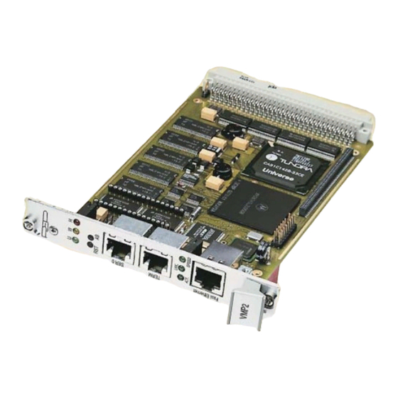
Summary of Contents for PEP Modular Computers VMP2
- Page 1 VMP2 Power PC-based CPU Board for VME Applications Manual ID: 24855, Rev. Index 02 November 2002 The product described in this manual is in compliance with all applied CE stan- dards.
-
Page 2: Imprint
PEP Modular Computers GmbH. Disclaimer: PEP Modular Computers GmbH rejects any liability for the cor- rectnesss and completeness of this manual as well as its suitabil- ity for any particular purpose. -
Page 3: Table Of Contents
1. Introduction ....................1 - 3 1.1 Board Introduction .................. 1 - 4 1.2 Board Overview ..................1 - 5 1.3 VMP2 Main Specifications ..............1 - 6 1.4 Applied Standards .................. 1 - 8 1.4.1 CE Compliance ................1 - 8 1.4.2 Mechanical Compliance .............. - Page 4 2.6.4 Front Panel LED’s ................2 - 19 Chapter 3. Installation ..................... 3 - 3 3.1 Board Installation ..................3 - 3 3.1.1 Front Panel I/O Connectors .............. 3 - 4 Page 0 - 4 © 2002 PEP Modular Computers GmbH ID 24855, Rev. 02...
- Page 5 4.3.5 IRQ Routing ................... 4 - 19 4.3.6 Real-time Clock ................4 - 20 4.3.7 EEPROM ..................4 - 21 4.3.8 Digital Temperature Sensor ............4 - 21 ID 24855, Rev. 02 © 2002 PEP Modular Computers GmbH Page 0 - 5...
- Page 6 Updating the NetBootLoader ............5 - 11 5.4.6.1 Updating With an Image Loaded Via an ftp Server ....5 - 11 5.4.6.2 Updating Via a Separate DIL FLASH ........5 - 11 Page 0 - 6 © 2002 PEP Modular Computers GmbH ID 24855, Rev. 02...
- Page 7 Annex B. VMP1-Post (Optional) ................... B - 3 Annex C. Optoisolation RS485 Module (Optional) ............C - 3 Annex D. JTAG Subsystem ..................D - 3 ID 24855, Rev. 02 © 2002 PEP Modular Computers GmbH Page 0 - 7...
- Page 8 E. CP320-TR1 (Optional) ................. E - 3 Annex Annex Annex Annex Annex F. CP320-TR2 (Optional) ................. F - 3 Annex G. PMC-HDD1 Module (Optional) ..............G - 3 Page 0 - 8 © 2002 PEP Modular Computers GmbH ID 24855, Rev. 02...
-
Page 9: List Of Tables
VMP2 Preface List of Tables VMP2 Main Specifications................1 - 6 Pin Assignment J1/P1 VME Connector CON1 .......... 2 - 10 Ethernet RJ45 Connector CON8 Pin Assignment ........2 - 11 Serial Port Connectors CON6 and CON7 Pin Assignment ....... 2 - 12 PCI Expansion Connector Pinout .............. - Page 10 E-3 CP320-TR1 Jumper Settings ..............E - 4 Serial Port Pinout ..................F - 4 G-1 Pinout of the PMC Connectors..............G - 4 G-2 IDE Hard Disk Drive Connector Pinout ............G - 5 Page 0 - 10 © 2002 PEP Modular Computers GmbH ID 24855, Rev. 02...
- Page 11 C-1 View of underside of RS485 Module ............C - 3 D-1 JTAG Chain Illustration ................D - 3 D-2 Resistor Positions on Reverse of VMP2 Board ..........D - 4 E-1 View of Underside of the CP320-TR1 Module..........E - 3 View of Underside of CP320-TR2 Module........... F - 4 G-1 PMC-HDD1 Module with Hard Disk Drive Attached ........
- Page 12 Preface VMP2 This page was intentionally left blank. Page 0 - 12 © 2002 PEP Modular Computers GmbH ID 24855, Rev. 02...
- Page 13 VMP2 Preface Preface ID 24855, Rev. 02 © 2002 PEP Modular Computers GmbH Page 0 - 13...
- Page 14 Preface VMP2 This page was intentionally left blank. ID 24855, Rev. 02 © 2002 PEP Modular Computers GmbH Page 0 - 14...
-
Page 15: Proprietary Note
This document contains information proprietary to PEP Modular Computers. It may not be copied or transmitted by any means, disclosed to others, or stored in any retrieval system or media without the prior written consent of PEP Modular Computers GmbH or one of its autho- rized agents. -
Page 16: Explanation Of Symbols
This symbol and title emphasize aspects the reader should read through carefully for his or her own advantage. PEP Advantage This symbol and title emphasize advantages or positive aspects of a product and/or procedure. Page 0 - 16 © 2002 PEP Modular Computers GmbH ID 24855, Rev. 02... -
Page 17: For Your Safety
They can cause short circuits and damage the batter- ies or conductive circuits on the board. ID 24855, Rev. 02 © 2002 PEP Modular Computers GmbH Page 0 - 17... - Page 18 In order to maintain PEP’s product warranty, this product must not be altered or modified in any way. Changes or modifications to the device, which are not explicitly approved by PEP Modular Computers and described in this manual or received from PEP Technical Support as a special handling instruction, will void your warranty.
-
Page 19: Two Year Warranty
PEP Modular Computers, and the remaining part of the original guarantee, or any new guarantee to cover the repaired or replaced items, will be transferred to cover the new or repaired items. - Page 20 Preface VMP2 This page was intentionally left blank. ID 24855, Rev. 02 © 2002 PEP Modular Computers GmbH Page 0 - 20...
- Page 21 VMP2 Introduction Chapter Introduction ID 24855, Rev. 02 © 2002 PEP Modular Computers GmbH Page 1 - 1...
- Page 22 VMP2 Introduction This page was intentionally left blank. Page 1 - 2 © 2002 PEP Modular Computers GmbH ID 24855, Rev. 02...
-
Page 23: Introduction
The VMP2 is based on the MPC8245, a highly integrated microprocessor containing a PowerPC MPC603e core. This is the 330 MHz version with a Floating Point Unit (FPU). -
Page 24: Board Introduction
VMP2 Introduction 1.1 Board Introduction The VMP2 is a VME PowerPC-based single-board computer specifically designed for use in highly integrated platforms with solid mechanical interfacing for a wide range of industrial environment applications. Some of the VMP2’s outstanding features are: •... -
Page 25: Board Overview
Introduction 1.2 Board Overview The VMP2 is a 3U VME CPU board featuring a powerful CPU (number cruncher). The design is based on the new highly integrated Motorola PowerPC processor MPC8245, which integrates a PCI interface and several peripherals inside one Chip. -
Page 26: Vmp2 Main Specifications
VMP2 Introduction 1.3 VMP2 Main Specifications Table 1-1: VMP2 Main Specifications VMP2 Specifications Operating System Initial boot loader with capability to load VxWorks and other Support Real-time operating systems ANSI/VITA 1-1994 for VME, approved April 10, 1995 VME Interface Support for A24: D16/D8 master and A24: D16/D8 slave... - Page 27 VMP2 Introduction Table 1-1: VMP2 Main Specifications (Continued) VMP2 Specifications Debug Interface JTAG/BDM VME Connector 96-pin VME connector Onboard Connectors 2 x RJ45 for RS232, 1 x RJ45 for Ethernet PMC carrier, future PCI based I/O board with PCI Expansion Modules...
-
Page 28: Applied Standards
VMP2 Introduction 1.4 Applied Standards 1.4.1 CE Compliance The PEP Modular Computers’ VME systems comply with the requirements of the follow- ing CE-relevant standards: • Emission EN50081-1 • Immission EN50082-2 • Electrical Safety EN60950 1.4.2 Mechanical Compliance • Mechanical Dimensions IEEE 1101.10... - Page 29 VMP2 Functional Description Chapter Functional Description ID 24855, Rev. 02 © 2002 PEP Modular Computers GmbH Page 2 - 1...
- Page 30 VMP2 Functional Description This page was intentionally left blank. Page 2 - 2 © 2002 PEP Modular Computers GmbH ID 24855, Rev. 02...
-
Page 31: Functional Description
DEBUG POWER Motorola JTAG/Test SUPPLY MPC 8245 interface DC/DC 200-332 MHz RESET GENERATION M41T56 EXPANSION CONNECTOR EEPROM FAST INTERFACE PCI Bus ETHERNET Tundra 82559ER Universe II ID 24855, Rev. 02 © 2002 PEP Modular Computers GmbH Page 2 - 3... -
Page 32: Front Panels
IO1 Module - note the different position of the LNK . LN K . SER 0 connector AC T. S PEE D ACT . S PEE D VMP1 VMP1 VMP1-IO1 Page 2 - 4 © 2002 PEP Modular Computers GmbH ID 24855, Rev. 02... -
Page 33: Board Layout
VMP2 Functional Description 2.3 Board Layout Figure 2-3: VMP2 Board (Front View) SDRAM MEMORY ABORT BANK 1 & RESET UART RJ45 (Serial) X BUS DC/DC DC/DC BUFFERS RJ45 (Term.) LOGIC PCI TO VME BRIDGE ETHERNET ETHERNET CON10 GOLDCAP CON11 PCI EXPANSION CONNECTOR... -
Page 34: Main Features
VMP2. 2.4.1 The VMP2 is based on the Motorola PowerPC processor MPC8245 which integrates a large number of peripherals, such as a PCI interface, PCI arbiter, Interrupt Controller, Memory Controller and multiple Timers. CPU speed is 330 MHz. - Page 35 (LSU), system register unit (SRU), and a branch processing unit (BPU) 16 kB instruction cache 16 kB data cache Lockable L1 cache - entire cache or on a per-way basis Dynamic power management ID 24855, Rev. 02 © 2002 PEP Modular Computers GmbH Page 2 - 7...
-
Page 36: Memory
Memory 2.4.2.1 System Memory (DRAM) The main memory of the VMP2 consists of SDRAM, ranging from 64 up to 256 MByte, soldered onto the board for mechanical stability. The VMP2 provides ECC support (optional) and a maximum memory speed of 132 MHz. -
Page 37: Board Interfaces
Compatibility with PEP VME backplane design and feature set • Compatibility with PEP backplane transceiver logic A table showing the pinout of the VME bus connector appears on the following page. ID 24855, Rev. 02 © 2002 PEP Modular Computers GmbH Page 2 - 9... -
Page 38: Vme Bus Connector Con1 Pinout
BG2IN BG2OUT SYSCLK BG3IN SYSFAIL BG3OUT BERR SYSRESET LWORD WRITE DTACK IACK IACKIN SERA IACKOUT SERB IRQ7 IRQ6 IRQ5 IRQ4 IRQ3 IRQ2 IRQ1 -12V +5VSTDBY +12V Page 2 - 10 © 2002 PEP Modular Computers GmbH ID 24855, Rev. 02... -
Page 39: Ethernet Interface And Connector Pinout
The connector used for the 100BaseTX Ethernet interface is an RJ45 connector. The signals on this connector are as follows Table 2-2: Ethernet RJ45 Connector CON8 Pin Assignment Pin Number Signal ID 24855, Rev. 02 © 2002 PEP Modular Computers GmbH Page 2 - 11... -
Page 40: Serial Interfaces And Connectorpinout
Register. Please refer to Table 4-14 in chapter 4. Additionally, a module is available from PEP which provides an optoisolated half/full duplex RS-485 interface. For this reason the onboard SER connector on the VMP2 baseboard is not equipped. Please contact PEP Support department for more informa- tion. -
Page 41: Pci Expansion Interface And Connector Pinout
VMP2 for adding special functionality which is not provided on the VMP2 main board or on the VME bus. All the PCI signals of the onboard PCI bus will be routed to this connector, so that a complete PCI bus is provided on this connector. In addition, almost the same number of ground and power pins (3.3V and 5V) as are on a... -
Page 42: Pci Expansion Connector (Con11) Pinout
C/BE3# SDA (I2C) +3.3V AD23 AD22 AD21 AD20 AD19 AD18 AD17 AD16 C/BE2# FRAME# IRDY# +3.3V TRDY# DEVSEL# STOP# LOCK# +3.3V Table continued on following page Page 2 - 14 © 2002 PEP Modular Computers GmbH ID 24855, Rev. 02... - Page 43 Pin Number Signal PERR# SERR# C/BE1# AD15 +3.3V AD14 AD13 AD12 AD11 AD10 C/BE0# +3.3V +12V -12V 1) Ground 4) +12V 2) +3.3V 5) -12V 3) +5V ID 24855, Rev. 02 © 2002 PEP Modular Computers GmbH Page 2 - 15...
-
Page 44: Serial Interface Expansion Connector And Pinout
Eprom (up to 512 kB) e.g. 27C040 M-Systems DiskOnChip 2000 (up to 288 MB) Note: For the pinout of this connector please see Chapter 4, section 4.2.1 Page 2 - 16 © 2002 PEP Modular Computers GmbH ID 24855, Rev. 02... -
Page 45: Debug Interface And Connector Pinout
2.5.8 Digital Temperature Sensor (LM75) The VMP2 also provides an onboard digital temperature sensor with a thermal watch- dog functionality (National Semiconductor LM75). This has various uses including, for example, calibration of the onboard RTC over a wider temperature range. -
Page 46: Special Board Features
Button and the NMI initiated from the watchdog. The positions of the Abort and Reset buttons on the Front Panel may be viewed in Figure 2-2. Page 2 - 18 © 2002 PEP Modular Computers GmbH ID 24855, Rev. 02... -
Page 47: Front Panel Led's
The general purpose LED’s are programmable via a register in the System Logic. 3 additional LED’s, all green, are provided to indicate Ethernet working conditions: • Ethernet Link Integrity • Ethernet Activity • Ethernet Speed ID 24855, Rev. 02 © 2002 PEP Modular Computers GmbH Page 2 - 19... - Page 48 VMP2 Functional Description This page was intentionally left blank. Page 2 - 20 © 2002 PEP Modular Computers GmbH ID 24855, Rev. 02...
- Page 49 VMP2 Installation Chapter Installation ID 24855, Rev. 02 © 2002 PEP Modular Computers GmbH Page 3 - 1...
- Page 50 VMP2 Installation This page was intentionally left blank. Page 3 - 2 © 2002 PEP Modular Computers GmbH ID 24855, Rev. 02...
-
Page 51: Installation
3.1 Board Installation Slot Selection The VMP2 is designed so that it may be used in any free slot of a 3U VME Backplane. It has an automatic first slot detection mechanism which configures it as a System Con- troller when placed in the far left slot. -
Page 52: Front Panel I/O Connectors
• Do not touch components, connector-pins or traces. • If working at an anti-static workbench with professional dis- charging equipment, please do not omit to use it. PEP Advantage The VMP2 is designed to be bootstrapped from the Flash device alone. 3.1.1 Front Panel I/O Connectors... - Page 53 VMP2 Configuration Chapter Configuration ID 24855, Rev. 02 © 2002 PEP Modular Computers GmbH Page 4 - 1...
- Page 54 VMP2 Configuration This page was intentionally left blank. Page 4 - 2 © 2002 PEP Modular Computers GmbH ID 24855, Rev. 02...
-
Page 55: Configuration
4.1.1 Bootstrap Loader / Socket Jumper J1 The Jumper J1 is used to select the memory position from which the VMP2 fetches its boot code. It determines the address position of the onboard Flash window and the Flash/SRAM expansion socket (DIL600, 32-pin). -
Page 56: Resistor Setting For Non-Standard Socket Devices
4.1.4 RS485 Termination (Onboard Interface Only) When the VMP2 is using the onboard RS485 interface and is the last on the RS485 bus, then the RS485 interface must provide termination resistance. The purpose of J3 is to enable this line termination resistor (130 R). -
Page 57: Pinouts
NVSRAM, M-Systems Disk-On-Chip, EPROM etc.). Table 4-4: DIL 32 Pinout for Various Devices 4Mbit Disk 4Mbit 4Mbit Disk 4Mbit Flash OnChip SRAM Eprom Eprom SRAM OnChip Flash ID 24855, Rev. 02 © 2002 PEP Modular Computers GmbH Page 4 - 5... -
Page 58: Serial Interface Expansion Connector (Con3)
VMP2 Configuration 4.2.2 Serial Interface Expansion Connector (CON3) Table 4-5: RS Expansion Connector Pinout Pin Number Function Function Pin Number RTSB +3.3V Page 4 - 6 © 2002 PEP Modular Computers GmbH ID 24855, Rev. 02... -
Page 59: Board Address Map
4.3.1 Address Map Overview The following figures illustrate the address mapping of the VMP2. Where the first figure describes the overall map, the second figure provides a more detailed map of the upper- most address area. The upper area address map depends on the configuration of the VMP2 memory expansion sockets and the requirements of the application. -
Page 60: Vme Address Area
VME bus slave address and VME IRQ mask are programmable inside the TUNDRA UNIVERSE II. Please refer to the VME slave manual chapter in the TUNDRA UNI- VERSE II manual and the BSP documentation. Page 4 - 8 © 2002 PEP Modular Computers GmbH ID 24855, Rev. 02... -
Page 61: Onboard Device Addresses
VMP2 Configuration 4.3.3 Onboard Device Addresses Figure 4-3: VMP2 Device Address Map soldered FLASH, Socket (512k page) 0xFFF8 0000 0xFFF8 0000 soldered FLASH, Socket (512k page) Reset Entry 0xFFFF 0100 0xFFF0 0000 0xFFF0 0000 reserved reserved 0xFFE8 0000 0xFFE8 0000... -
Page 62: Special Registers Overview
Event Register 0xFFE0 001C Board/Logic Revision 0xFFE0 001E 4.3.4.2 Board ID Register The Board ID can be used to identify the VMP2 in a VME system. The value for the VMP2 is 01h. Table 4-7: Board ID Register REGISTER NAME ACCESS... -
Page 63: Software Compatibility Id
0x00 and will be incremented with each change in hardware (software sensitive only). Table 4-8: Software Compatibility ID REGISTER NAME ACCESS SOFTWARE COMPATIBILITY ID ADDRESS 0xFFE0 0012 BIT POSITION CONTENT DEFAULT ID 24855, Rev. 02 © 2002 PEP Modular Computers GmbH Page 4 - 11... -
Page 64: Memory Configuration Register
Flash memory may only be accessed through a 512 kB window; this is the only way to address a larger size Flash memory. Using bits FB0..FB3, 16 Flash banks can be selected (16x512 kB = 8 MB). The default value on startup of the VMP2 is 0x00. Table 4-10: Flash Bank Select Register... -
Page 65: Watchdog Control Register
Causes generation of a non-maskable interrupt upon Watchdog timeout Watchdog timer disabled Watchdog timer enabled Note... WD_EN Once the Watchdog timer is enabled it cannot be disabled except by resetting the system. ID 24855, Rev. 02 © 2002 PEP Modular Computers GmbH Page 4 - 13... -
Page 66: Control Register
When setting bit 7 the user must ensure that the corresponding interface is also an RS485. A mismatch will risk damage to the VMP2 and/or the application. Page 4 - 14 © 2002 PEP Modular Computers GmbH ID 24855, Rev. 02... -
Page 67: Event Register
Indicates that the Abort switch has not been pressed Indicates that the Abort switch has been pressed Reserved Reserved Reserved Reserved This bit is used by the bootstrap loader ID 24855, Rev. 02 © 2002 PEP Modular Computers GmbH Page 4 - 15... -
Page 68: Board / Logic Revision Register
0x00 for the initial board prototypes and will be incremented with each redesign / logic release. Table 4-14: Board Logic / Revision Register REGISTER NAME ACCESS BOARD LOGIC/REVISION ADDRESS 0xFFE0 001E BIT POSITION CONTENT DEFAULT Page 4 - 16 © 2002 PEP Modular Computers GmbH ID 24855, Rev. 02... -
Page 69: Uart A / Registers
Enhanced Mode Select Enhanced Mode Select Register FFe0 0007 Register Xon-1 Xon-1 FFe0 0004 Xon-2 Xon-2 FFe0 0005 Xoff-1 Xoff-1 FFe0 0006 Xoff-2 Xoff-2 FFe0 0007 ID 24855, Rev. 02 © 2002 PEP Modular Computers GmbH Page 4 - 17... -
Page 70: Uart B / Registers
Enhanced mode select register Enhanced mode select register 0xFFE0 000F Xon-1 Xon-1 0xFFE0 000C Xon-2 Xon-2 0xFFE0 000D Xoff-1 Xoff-1 0xFFE0 000E Xoff-2 Xoff-2 0xFFE0 000F Page 4 - 18 © 2002 PEP Modular Computers GmbH ID 24855, Rev. 02... -
Page 71: Irq Routing
LINT3# / VME Interrupt level 5 and 6 S_IRQ12 LINT4# / VME Interrupt level 7 + SYSFAIL S_IRQ13 LINT5# / VME ACFAIL S_IRQ14 LINT6# / 4 location monitors S_IRQ15 LINT7# / 4 mailboxes ID 24855, Rev. 02 © 2002 PEP Modular Computers GmbH Page 4 - 19... -
Page 72: Real-Time Clock
When the RTC has once been stopped due to low voltage, it is necessary to re-initialize the “Seconds” “Minutes” and “Hours” reg- isters before it will run again. Page 4 - 20 © 2002 PEP Modular Computers GmbH ID 24855, Rev. 02... -
Page 73: Eeprom
The EEPROM uses the I2C address 0x90. For more detailed information please refer to the manuals for the National Semiconduc- tor LM75 and the MOTOROLA MPC8245 (I2C bus). ID 24855, Rev. 02 © 2002 PEP Modular Computers GmbH Page 4 - 21... - Page 74 VMP2 Configuration This page was intentionally left blank. Page 4 - 22 © 2002 PEP Modular Computers GmbH ID 24855, Rev. 02...
-
Page 75: Netbootloader
VMP2 NetBootLoader Chapter NetBootLoader ID 24855, Rev. 02 © 2002 PEP Modular Computers GmbH Page 5 - 1... - Page 76 NetBootLoader VMP2 This page was intentionally left blank. Page 5 - 2 © 2002 PEP Modular Computers GmbH ID 24855, Rev. 02...
-
Page 77: General Operation
“abort” command via the TERM interface, or by performing a successful telnet login via the Ethernet interface. If the operator does not intervene, the boot operation is continued after the boot wait time has been exceeded. ID 24855, Rev. 02 © 2002 PEP Modular Computers GmbH Page 5 - 3... -
Page 78: Abt (Abort) Switch
The command title (CMD TITLE) is expressed in capital letters and is not the same as the syntax of the command. The command syntax is always written using small letters Page 5 - 4 © 2002 PEP Modular Computers GmbH ID 24855, Rev. 02... -
Page 79: Netbootloader Control
Display system information Memory Display memory contents Applies to all visible memory Display Display PCI device information PING Verify network status Version Display version number of NetBootLoader ID 24855, Rev. 02 © 2002 PEP Modular Computers GmbH Page 5 - 5... -
Page 80: Ftp Server Access
Table 5-5: Motorola S-Records Commands CMD TITLE ALIAS FUNCTION REMARKS SLoad Download Motorola S-Records Uses data buffer as target Page 5 - 6 © 2002 PEP Modular Computers GmbH ID 24855, Rev. 02... -
Page 81: Operating The Netbootloader
CPU board, the system must either be cold started or the operator must issue a “reset” command. In either event, the NetBootLoader is restarted and the boot operation begins anew. ID 24855, Rev. 02 © 2002 PEP Modular Computers GmbH Page 5 - 7... -
Page 82: Netbootloader Configuration
This command is used to set the password used by the NetBootLoader for the operation of the telnet interface. No password is required for access from the TERM interface. Page 5 - 8 © 2002 PEP Modular Computers GmbH ID 24855, Rev. 02... -
Page 83: Telnet Login
If an offset is specified, the image will be programmed exactly at this offset without adding length or CRC information. This option is intended for the storing of configuration information which is required to be located in FLASH. ID 24855, Rev. 02 © 2002 PEP Modular Computers GmbH Page 5 - 9... -
Page 84: Programming An Application
If necessary, the base address can be modified with the -o option of the “sl” command. Page 5 - 10 © 2002 PEP Modular Computers GmbH ID 24855, Rev. 02... -
Page 85: Updating The Netbootloader
FLASH. In this case, the boot operation must be started with the Boot Jumper inserted (boot from DIL FLASH). ID 24855, Rev. 02 © 2002 PEP Modular Computers GmbH Page 5 - 11... -
Page 86: Uploading A Flash Area
If it is necessary to relocate the image to another address after download, simply add a small assembly routine at the beginning of the code which will move the image to the correct address. Page 5 - 12 © 2002 PEP Modular Computers GmbH ID 24855, Rev. 02... -
Page 87: Commands
(U) flashes at the rate of two times a second. Therefore, if the boot wait is set to 1 second the LED will only flash two times. ID 24855, Rev. 02 © 2002 PEP Modular Computers GmbH Page 5 - 13... - Page 88 DESCRIPTION: An ftp server session which has been established with the command “login” is terminated with the command “bye”. FUNCTION: Change the current ftp server directory Page 5 - 14 © 2002 PEP Modular Computers GmbH ID 24855, Rev. 02...
- Page 89 “check” command is used to verify that the current application image in FLASH is valid. USAGE: Veriy valid application is stored in FLASH COMMAND / RESPONSE: check Check userimage CRC: ok ID 24855, Rev. 02 © 2002 PEP Modular Computers GmbH Page 5 - 15...
- Page 90 In both cases, the new image is checked for validity. If an image is invalid, the update is aborted. Additionally, the operation must be confirmed by typing the word “yes”. Any other or no input will cancel the operation. Page 5 - 16 © 2002 PEP Modular Computers GmbH ID 24855, Rev. 02...
- Page 91 Download file from ftp server SYNTAX: get <filename> where: command <filename> parameter: string name of image file to be downloaded, or path and name of image file to be downloaded ID 24855, Rev. 02 © 2002 PEP Modular Computers GmbH Page 5 - 17...
- Page 92 The command “info” is used to display an information summary for the running system. The CPU type, the board type, and the detected FLASH layout are displayed. Page 5 - 18 © 2002 PEP Modular Computers GmbH ID 24855, Rev. 02...
- Page 93 Without parameters, the FLASH is programmed using the contents of the data buffer. If no image is available in the data buffer, the FLASH programming is terminated. ID 24855, Rev. 02 © 2002 PEP Modular Computers GmbH Page 5 - 19...
- Page 94 Program FLASH from data buffer to offset 0xF4240 COMMAND / RESPONSE (none): lf -o=f4240 Program FLASH from visible address at 0x87000000 for length of 0x123456 COMMAND / RESPONSE (none): lf -m=87000000 -l=123456 Page 5 - 20 © 2002 PEP Modular Computers GmbH ID 24855, Rev. 02...
- Page 95 COMMAND / RESPONSE: login 192.168.47.12 johndoe mypassword (Response is dependent on the server accessed) L O G O U T FUNCTION: Terminate telnet session with NetBootLoader ID 24855, Rev. 02 © 2002 PEP Modular Computers GmbH Page 5 - 21...
- Page 96 If issued again without the “<adr>” parameter, the display starts with the end address of the previous display. Data is displayed as hexadecimal 32-bit words and as ASCII dump. Page 5 - 22 © 2002 PEP Modular Computers GmbH ID 24855, Rev. 02...
- Page 97 CRC. This is done automatically. Only in the event that the Ethernet interface does not properly initialize, may it be necessary to re-enter the parameters using the “-f” option. ID 24855, Rev. 02 © 2002 PEP Modular Computers GmbH Page 5 - 23...
- Page 98 (The old password must be known) Set password when the old password is not known COMMAND / RESPONSE: NetBtLd> passwd New Password: ***** Type again : ***** NetBtLd> Page 5 - 24 © 2002 PEP Modular Computers GmbH ID 24855, Rev. 02...
- Page 99 <parity> parameter: string: “n” (none), “o” (odd), “e” (even) defines parity to be used <stops> parameter: value: number: “1”, “2” defines number of stop bits ID 24855, Rev. 02 © 2002 PEP Modular Computers GmbH Page 5 - 25...
- Page 100 Set the bits per character parameter of “SER0” to 7 COMMAND / RESPONSE (none): pf ser0 //7 Set the stop bits parameter of “SER0” to 2 COMMAND / RESPONSE (none): pf ser0 ///2 Page 5 - 26 © 2002 PEP Modular Computers GmbH ID 24855, Rev. 02...
- Page 101 COMMAND / RESPONSE: ping 192.192.158.7 Send ten packets, 100 bytes long, and wait two seconds between packets COMMAND / RESPONSE: ping 192.192.158.7 -c 10 -s 100 -w 2 ID 24855, Rev. 02 © 2002 PEP Modular Computers GmbH Page 5 - 27...
- Page 102 If a ftp connection has been established with the “login” command, the command “pwd” is used to display the complete path of the current directory on the ftp server. FUNCTION: Reset the system SYNTAX: Page 5 - 28 © 2002 PEP Modular Computers GmbH ID 24855, Rev. 02...
- Page 103 USAGE: Store 64 kB of FLASH contents to the data buffer beginning at an offset of 1 MB COMMAND / RESPONSE (none): sf -o=100000 -l=10000 ID 24855, Rev. 02 © 2002 PEP Modular Computers GmbH Page 5 - 29...
- Page 104 Download S-Records to data buffer and reduce each record’s address by 0x10000. COMMAND / RESPONSE (none): sl -o=10000 FUNCTION: Display version number SYNTAX: DESCRIPTION: The command “ver” displays the actual version number of the NetBootLoader. Page 5 - 30 © 2002 PEP Modular Computers GmbH ID 24855, Rev. 02...
- Page 105 VMP2 VMP1-IO1 Module (Optional) Appendix VMP1-IO1 Module (Optional) ID 24855, Rev. 02 © 2002 PEP Modular Computers GmbH Page A - 1...
-
Page 106: Vmp1-Io1 Module (Optional)
VMP2 VMP1-IO1 Module (Optional) This page was intentionally left blank. Page A - 2 © 2002 PEP Modular Computers GmbH ID 24855, Rev. 02... -
Page 107: Overview
PMC modules in a 3U environment. A special feature of the VMP2 is the ability to cascade two of these IO1 modules on top of one another. This means that the VMP2 is able to carry any two PMC modules. Tre- mendous advantages in terms of expandability and flexibility are thus made available to the user as a result of the addition of this capability to the board’s many outstanding fea-... -
Page 108: Board Interfaces
PCI Specification Rev. 2.1. PMC Interface The PMC interface provides an easy way to extend the VMP2 via the wide array of inter- faces and functions which are available on PMC modules produced by the entire range of PMC vendors. -
Page 109: Board Layout
The VMP1-IO1 has two onboard connectors (CON9 and CON10) which provide all the PCI signals and the power supply for the PMC module. Figure A-1: Board Layout (Front View) MAGNIFIED DC/DC PCI EXPANSION CONNECTOR ID 24855, Rev. 02 © 2002 PEP Modular Computers GmbH Page A - 5... -
Page 110: Vmp1-Io1 Front Panel
A.4 VMP1-IO1 Front Panel Figure A-2: VMP1-IO1 Front Panel VMP1-IO1 The VMP1-IO1 front panel is provided with a window for the insertion of a PMC module bezel. Page A - 6 © 2002 PEP Modular Computers GmbH ID 24855, Rev. 02... -
Page 111: Technical Specifications
IEC68-2-64 Shocks: Permanent Shocks IEC68-2-29 Single Shock IEC68-2-27 Single-height Eurocard: Board Dimensions 100 mm x 160 mm 1 x 4 HP slot Board Weight 114 grams ID 24855, Rev. 02 © 2002 PEP Modular Computers GmbH Page A - 7... -
Page 112: Board Installation
6 mm) to secure the board to the VMP2 PMC Module Installation Place the EMC gasket on the bezel of your PMC-Module Push the PMC bezel into the window of the front-panel of the VMP2 and plug the connectors together. ×... - Page 113 VMP2 VMP1-IO1 Module (Optional) Figure A-3: Installation Diagrams PMC module VMP1-IO1 Front Panel VMP1-IO1 10mm stand-off PMC bezel 4 *M2.5 *6mm screws ID 24855, Rev. 02 © 2002 PEP Modular Computers GmbH Page A - 9...
-
Page 114: Pinouts
Ground IRDY# DEVSEL# Ground LOCK# SDONE# SBO# Ground V(I/O) AD[15] AD[12] AD[11] AD[09] Ground C/BE[0]# AD[06] AD[05] AD[04] Ground V(I/O) AD[03] AD[02] AD[01] AD[00] Ground REQ64# Page A - 10 © 2002 PEP Modular Computers GmbH ID 24855, Rev. 02... -
Page 115: Jn2 (Con5) Pin Assignment
PERR# Ground +3.3V SERR# C/BE[1]# Ground AD[14] AD[13] Ground AD[10] AD[08] +3.3V AD[07] PMC-RSVD +3.3V PMC-RSVD PMC-RSVD Ground PMC-RSVD PMC-RSVD Ground PMC-RSVD ACK64# +3.3V Ground PMC-RSVD ID 24855, Rev. 02 © 2002 PEP Modular Computers GmbH Page A - 11... -
Page 116: Jumper Setting
VMP1-IO1 Module (Optional) A.8 Jumper Setting The jumper settings of the IO1 module depend on the module’s position relative to the VMP2 and other modules, if any (please see Figure A4 below). Table A-4: IO1 Jumper Settings for Different Module Positions IDSEL... - Page 117 VMP2 VMP1-Post (Optional) Appendix VMP1-Post (Optional) ID 24855, Rev. 02 © 2002 PEP Modular Computers GmbH Page B - 1...
-
Page 118: Vmp1-Post (Optional)
VMP2 VMP1-Post (Optional) This page was intentionally left blank. Page B - 2 © 2002 PEP Modular Computers GmbH ID 24855, Rev. 02... - Page 119 The programmer can, therefore, define his own debug code and send it to the VMP2 by making a byte write command to the first address of the socket memory area. This address is 0xFFF0 0000 when the boot jumper J1 of the VMP2 is set and 0xFFF8 0000 when the boot jumper is open.
- Page 120 VMP2 VMP1-Post (Optional) Board Diagrams Figure B-1: Plan and Profile Views of VMP1-Post Module PLAN Number Display PROFILE NUMBER DISPLAY Higher Power Lower Power Page B - 4 © 2002 PEP Modular Computers GmbH ID 24855, Rev. 02...
- Page 121 VMP2 Optoisolation RS485 Module (Optional) Appendix Appendix Optoisolation RS485 Module (Optional) ID 24855, Rev. 02 © 2002 PEP Modular Computers GmbH Page C - 1...
-
Page 122: Optoisolation Rs485 Module (Optional)
VMP2 Optoisolation RS485 Module (Optional) This page was intentionally left blank. Page C - 2 © 2002 PEP Modular Computers GmbH ID 24855, Rev. 02... -
Page 123: View Of Underside Of Rs485 Module
Users who require an optoisolated version of the VMP2 are supplied with a customized VMP2 on which the standard RJ45 connector is omitted and also with this module which comes with a substitute RJ45 connector routed through optoisolation circuitry on the module. - Page 124 VMP2 Optoisolation RS485 Module (Optional) This page was intentionally left blank. Page C - 4 © 2002 PEP Modular Computers GmbH ID 24855, Rev. 02...
-
Page 125: Jtag Subsystem
VMP2 JTAG Subsystem Appendix Appendix JTAG Subsystem ID 24855, Rev. 02 © 2002 PEP Modular Computers GmbH Page D - 1... - Page 126 VMP2 JTAG Subsystem This page was intentionally left blank. Page D - 2 © 2002 PEP Modular Computers GmbH ID 24855, Rev. 02...
- Page 127 D. JTAG Subsystem Description All the JTAG capable devices on the VMP2 can be accessed through the onboard JTAG chain. The factory setting of the chain is such that only the onboard logic is in the chain. If it is required to access the Processor via the JTAG chain a different setting must be used (some resistors must be reset).
- Page 128 If EMULATOR access to the MPC8245 is required it must be ensured that R94 and R183 are set and also that R104 and R180 are removed (all resistors are 0R). Figure D-2: Resistor Positions on Reverse of VMP2 Board SDRAM MEMORY...
- Page 129 VMP2 CP320-TR1 (Optional) Appendix CP320-TR1 (Optional) ID 24855, Rev. 02 © 2002 PEP Modular Computers GmbH Page E - 1...
- Page 130 VMP2 CP320-TR1 (Optional) This page was intentionally left blank. Page E - 2 © 2002 PEP Modular Computers GmbH ID 24855, Rev. 02...
-
Page 131: Serial Port Pinout
Table E-2: Serial Port Pinout RS485 CON6 SIGNAL RJ45 HALF-DUPLEX FULL-DUPLEX (Serial) -RxD +TRXD -TxD +RxD -TRXD +TxD Refer to the Functional Description chapter for the pinout of CON3. ID 24855, Rev. 02 © 2002 PEP Modular Computers GmbH Page E - 3... - Page 132 VMP2 CP320-TR1 (Optional) Table E-3: CP320-TR1 Jumper Settings JUMPER SETTING FUNCTION 120 ohm termination, full-duplex 120 ohm termination, Open half-duplex No termination Open Open Page E - 4 © 2002 PEP Modular Computers GmbH ID 24855, Rev. 02...
- Page 133 VMP2 CP320-TR2 (Optional) Appendix CP320-TR2 (Optional) ID 24855, Rev. 02 © 2002 PEP Modular Computers GmbH Page F - 1...
- Page 134 CP320-TR2 (Optional) VMP2 This page was intentionally left blank. Page F - 2 © 2002 PEP Modular Computers GmbH ID 24855, Rev. 02...
- Page 135 The module has been designed so that it does not increase the board width, which remains unchanged at 4HP with the module in place. View of Underside of the CP320- TR2 Module. ID 24855, Rev. 02 © 2002 PEP Modular Computers GmbH Page F - 3...
-
Page 136: Serial Port Pinout
Serial Port Pinout Table F-1: Serial Port Pinout RS232 Signal CON3 ISO-GND CON6 RJ45 (Serial) Please note that this diagram is not to scale with other board diagrams Page F - 4 © 2002 PEP Modular Computers GmbH ID 24855, Rev. 02... - Page 137 VMP2 PMC-HDD1 Module (Optional) Appendix PMC-HDD1 Module (Optional) ID 24855, Rev. 02 © 2002 PEP Modular Computers GmbH Page G - 1...
- Page 138 PMC-HDD1 Module (Optional) VMP2 This page was intentionally left blank. Page G - 2 © 2002 PEP Modular Computers GmbH ID 24855, Rev. 02...
- Page 139 • The capacity of the module is defined by the hard drive in use. Figure G-1: PMC-HDD1 Module with Hard Disk Drive Attached HARD DISK DRIVE UNIT PMC-HDD1 ID 24855, Rev. 02 © 2002 PEP Modular Computers GmbH Page G - 3...
- Page 140 Signal Signal Signal Signal +3.3V Signal Signal Ground Signal Ground V (I/O) Signal Signal Signal Signal Signal Ground Signal Signal Signal +3.3V Ground Signal Ground Signal Page G - 4 © 2002 PEP Modular Computers GmbH ID 24855, Rev. 02...
- Page 141 Ground signal IDEIRQ Interrupt request Address 1 Address 0 Address 2 HCS0 HD select 0 HCS1 HD select 1 Ground signal 5V power 5V power Ground signal ID 24855, Rev. 02 © 2002 PEP Modular Computers GmbH Page G - 5...
- Page 142 PMC-HDD1 Module (Optional) VMP2 This page was intentionally left blank. Page G - 6 © 2002 PEP Modular Computers GmbH ID 24855, Rev. 02...
Need help?
Do you have a question about the VMP2 and is the answer not in the manual?
Questions and answers