Bose T1 ToneMatch Service Manual
Audio engine
Hide thumbs
Also See for T1 ToneMatch:
- Owner's manual (62 pages) ,
- Quick setup manual (2 pages) ,
- Owner's manual (2 pages)

Subscribe to Our Youtube Channel
Related Manuals for Bose T1 ToneMatch


Summary of Contents for Bose T1 ToneMatch
- Page 1 ® T1 ToneMatch Audio Engine US/Canada, European, UK and Australian Versions ©2010 Bose Corporation Service Manual Reference Number 296137-SM Rev. 01 Electronic Copy Only...
-
Page 2: Table Of Contents
Audio Engine (see Figure 1) ..........8 Figure 1. T1 ToneMatch Audio Engine Packaging View ..............8 Main Part List, T1 ToneMatch Audio Engine (see Figure 2) ............9 Figure 2. T1 ToneMatchTM Audio Engine Exploded View ..............10 Electrical Part Lists ........................11-39 Input/Output PCB Assembly .....................11-14... -
Page 3: Safety Information
THE PURPOSE OF SERVICING THE IDENTIFIED BOSE PRODUCT BY AN AUTHORIZED BOSE SERVICE CENTER OR OWNER OF THE BOSE PRODUCT, AND SHALL NOT BE REPRODUCED OR USED FOR ANY OTHER PURPOSE. Warranty The Bose T1 ToneMatch Audio Engine is covered by a limited 2-year transferable warranty. -
Page 4: Specifications
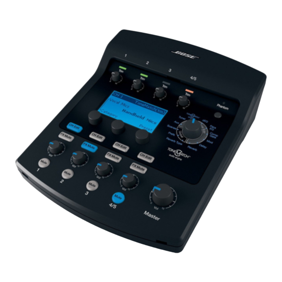
The T1 ToneMatch audio engine can be used with a Bose L1™ model II or model I system. When used with the Bose L1 model II or model I system, the T1 allows you to control the sound of your instrument as well as the output of the entire system. Using proprietary ToneMatch presets and associated zEQ tonal adjustments, the T1 enables you to preserve the natural sound of instruments or vocal microphones when amplified. - Page 5 Front Panel Controls and Indicators The control panel provides all the necessary controls and indicators for operation. 1. Input signal/clip LEDs (1-4/5) – Displays the input signal status in color: Green indicates the presence of an input signal, yellow indicates a signal near clipping, and red indicates clipping. 2.
- Page 6 Rear Connection Panel The rear panel provides all input/output connections. 1. IN – Analog input channels 1-3. Accepts XLR balanced cables for microphones, or ¼” TRS balanced or TS unbalanced cables for high-impedance inputs such as guitars. 2. Preamp OUT – Preamp outputs for channels 1-3. Accepts ¼” TRS balanced or TS unbal- anced cables.
-
Page 7: Electrostatic Discharge Sensitive (Esds) Device Handling
Accessories ® Description Bose Part Number Vendor Part Number T1 ToneMatch Power Supply 042533 Ethercon Cable Assy 042536 svc-sien11+cable Carry Bag Accessory 042534 svc-sien11+bag Microphone Stand Bracket 042535 T1 ToneMatch audio engine ToneMatch audio engine power supply microphone stand bracket... -
Page 8: Packaging Part List, T1 Tonematch
298750 4155-2721+0 RETENTION SCREW 298751 4155-2731+0 POLYBAG 1497-2812+0 L2 MOUNTING ARM 298749 4135-7071+0 POLYBAG 1497-7222+0 GIFT BOX (CARTON) 298754 1481-0701+1 1 2 3 4 5 4 6 10 11 12 13 14 Figure 1. T1 ToneMatch Audio Engine Packaging View... -
Page 9: Main Part List, T1 Tonematch Audio Engine (See Figure 2)
Main Part List T1 ToneMatch ® Audio Engine (see Figure 2) ® Item Description Bose Part Vendor Part Qty. Note Number Number Number PANEL, REAR, I/O 298733 1406-3101+0 HOUSING, TOP 298730 1468-0401+1 HOUSING, BOTTOM 298731 1468-0501+1 LID ASSY, CONSISTS OF ITEMS... - Page 10 ® Figure 2. T1 ToneMatch Audio Engine Exploded View...
-
Page 11: Electrical Part Lists
Electrical Part List Input/Output PCB Assembly Resistors Reference Description Vendor Part Note Designator Number 100K, RMG, 0603, 1/16W, 1% 4723-104A+P 100K, RMG, 0603, 1/16W, 1% 4723-104A+P 0 OHM, RMG, 0603, 1/16W, 5% 4723-000J+P 0 OHM, RMG, 0603, 1/16W, 5% 4723-000J+P 0 OHM, RMG, 0603, 1/16W, 5% 4723-000J+P 0 OHM, RMG, 0603, 1/16W, 5%... - Page 12 Electrical Part List Input/Output PCB Assembly Resistors (continued) Reference Description Vendor Part Note Designator Number R128 10K, RMG, 0603/1608, 1/16W, 1% 4723-103A+P R139 10K, RMG, 0603/1608, 1/16W, 1% 4723-103A+P R223 47K, RMG, 0603/1608, 1/16W, 5% 4723-473J+P R224 47K, RMG, 0603/1608, 1/16W, 5% 4723-473J+P R225 47K, RMG, 0603/1608, 1/16W, 5%...
- Page 13 Electrical Part List Input/Output PCB Assembly Capacitors (continued) Reference Description Vendor Part Note Designator Number 100pF, CC, 0603/1608, 50V, 5%, 1X2 150F-101J+P-AC 100pF, CC, 0603/1608, 50V, 5%, 1X2 150F-101J+P-AC 100pF, CC, 0603/1608, 50V, 5%, 1X2 150F-101J+P-AC 100pF, CC, 0603/1608, 50V, 5%, 1X2 150F-101J+P-AC 100pF, CC, 0603/1608, 50V, 5%, 1X2 150F-101J+P-AC...
- Page 14 Electrical Part List Input/Output PCB Assembly Capacitors (continued) Reference Description Vendor Part Note Designator Number C239 0.1uF, CC, 0603/1608, 50V, 10%, 1x2 150F-104K+P-AC C240 100pF, CC, 0603/1608, 50V, 5%, 1X2 150F-101J+P-AC C241 100pF, CC, 0603/1608, 50V, 5%, 1X2 150F-101J+P-AC C242 0.1uF, CC, 0603/1608, 50V, 10%, 1x2 150F-104K+P-AC C243...
-
Page 15: Digital Signal Processor (Dsp) Pcb Assembly
Electrical Part List Digital Signal Processor (DSP) PCB Assembly Resistors Reference Description Vendor Part Note Designator Number 100K, RMG, 0603, 1/16W, 1% 4723-104A+P 100K, RMG, 0603, 1/16W, 1% 4723-104A+P 10M, RMG, 0603/1608, 1/16W, 5% 4723-106J+P 100 OHM, RMG, 0603/1608, 1/16W, 5% 4723-101J+P 100 OHM, RMG, 0603/1608, 1/16W, 5% 4723-101J+P... - Page 16 Electrical Part List Digital Signal Processor (DSP) PCB Assembly Resistors (continued) Reference Description Vendor Part Note Designator Number 10K, RMG, 0603/1608, 1/16W, 1% 4723-103A+P 10K, RMG, 0603/1608, 1/16W, 1% 4723-103A+P 10K, RMG, 0603/1608, 1/16W, 1% 4723-103A+P 10K, RMG, 0603/1608, 1/16W, 1% 4723-103A+P 10K, RMG, 0603/1608, 1/16W, 1% 4723-103A+P...
- Page 17 Electrical Part List Digital Signal Processor (DSP) PCB Assembly Resistors (continued) Reference Description Vendor Part Note Designator Number R109 1K, RMG, 0603/1608, 1/16W, 1% 4723-102A+P R110 0 OHM, RMG, 0603, 1/16W, 5% 4723-000J+P-R R112 1K, RMG, 0603/1608, 1/16W, 1% 4723-102A+P R113 0 OHM, RMG, 0603, 1/16W, 5% 4723-000J+P-R...
- Page 18 Electrical Part List Digital Signal Processor (DSP) PCB Assembly Resistors (continued) Reference Description Vendor Part Note Designator Number R158 3.3K, RMG, 0603/1608, 1/16W, 1% 4723-332A+P R162 10K, RMG, 0603/1608, 1/16W, 5% 4723-103J+P R163 10K, RMG, 0603/1608, 1/16W, 5% 4723-103J+P R164 10K, RMG, 0603/1608, 1/16W, 5% 4723-103J+P R167...
- Page 19 Electrical Part List Digital Signal Processor (DSP) PCB Assembly Resistors (continued) Reference Description Vendor Part Note Designator Number R210 634 OHM, 0603, RMG, 1/16W, 1% 4723-6340+P R211 634 OHM, 0603, RMG, 1/16W, 1% 4723-6340+P R212 634 OHM, 0603, RMG, 1/16W, 1% 4723-6340+P R213 4.7K, RMG, 0603/1608, 1/16W, 5%...
- Page 20 Electrical Part List Digital Signal Processor (DSP) PCB Assembly Resistors (continued) Reference Description Vendor Part Note Designator Number R276 100K, RMG, 0603/1608, 1/16W, 5% 4723-104J+P R277 4.42K, RMG, 0603, 1/16W, 1% 4723-4421+P R278 4.42K, RMG, 0603, 1/16W, 1% 4723-4421+P R279 100K, RMG, 0603/1608, 1/16W, 5% 4723-104J+P R280...
- Page 21 Electrical Part List Digital Signal Processor (DSP) PCB Assembly Resistors (continued) Reference Description Vendor Part Note Designator Number R326 1.5K, RMG, 1206, 1/8W, 5% 4721-152J+6 R327 30K, RMG, 0603/1608, 1/16W, 5% 4723-303J+P R328 30K, RMG, 0603/1608, 1/16W, 5% 4723-303J+P R329 30K, RMG, 0603/1608, 1/16W, 5% 4723-303J+P R330...
- Page 22 Electrical Part List Digital Signal Processor (DSP) PCB Assembly Resistors (continued) Reference Description Vendor Part Note Designator Number R372 4.99K, RMG, 0603, 1/16W, 1% 4723-4991+P R373 4.99K, RMG, 0603, 1/16W, 1% 4723-4991+P R374 4.99K, RMG, 0603, 1/16W, 1% 4723-4991+P R375 4.99K, RMG, 0603, 1/16W, 1% 4723-4991+P R376...
- Page 23 Electrical Part List Digital Signal Processor (DSP) PCB Assembly Resistors (continued) Reference Description Vendor Part Note Designator Number R419 3.3K, RMG, 0603/1608, 1/16W, 1% 4723-332A+P R420 3.3K, RMG, 0603/1608, 1/16W, 1% 4723-332A+P R421 10 OHM, RMG, 1206, 1/4W, 5% 4725-100J+6 R501 100 OHM, RMG, 0603/1608, 1/16W, 5% 4723-101J+P...
- Page 24 Electrical Part List Digital Signal Processor (DSP) PCB Assembly Resistors (continued) Reference Description Vendor Part Note Designator Number R556 10K, RMG, 0603/1608, 1/16W, 5% 4723-103J+P R557 10K, RMG, 0603/1608, 1/16W, 5% 4723-103J+P R558 10K, RMG, 0603/1608, 1/16W, 5% 4723-103J+P R559 10K, RMG, 0603/1608, 1/16W, 5% 4723-103J+P R560...
- Page 25 Electrical Part List Digital Signal Processor (DSP) PCB Assembly Capacitors Reference Description Vendor Part Note Designator Number 1000pF, CC, 0603/1608, 50V, 10%, 1X2 150F-102K+P-AC 0.01uF, CC, 0603, 50V, 10%, 1x2 150F-103K+P-AC 0.01uF, CC, 0603, 50V, 10%, 1x2 150F-103K+P-AC 100pF, CC, 0603/1608, 50V, 5%, 1X2 150F-101J+P-AC 0.01uF, CC, 0603, 50V, 10%, 1x2 150F-103K+P-AC...
- Page 26 Electrical Part List Digital Signal Processor (DSP) PCB Assembly Capacitors (continued) Reference Description Vendor Part Note Designator Number 0.01uF, CC, 0603, 50V, 10%, 1x2 150F-103K+P-AC 1000pF, CC, 0603/1608, 50V, 10%, 1X2 150F-102K+P-AC 1000pF, CC, 0603/1608, 50V, 10%, 1X2 150F-102K+P-AC 1000pF, CC, 0603/1608, 50V, 10%, 1X2 150F-102K+P-AC 1000pF, CC, 0603/1608, 50V, 10%, 1X2 150F-102K+P-AC...
- Page 27 Electrical Part List Digital Signal Processor (DSP) PCB Assembly Capacitors (continued) Reference Description Vendor Part Note Designator Number C100 100pF, CC, 0603/1608, 50V, 5%, 1X2 150F-101J+P-AC C102 100pF, CC, 0603/1608, 50V, 5%, 1X2 150F-101J+P-AC C104 100pF, CC, 0603/1608, 50V, 5%, 1X2 150F-101J+P-AC C106 470pF, CC, 0603, 50V, 5%...
- Page 28 Electrical Part List Digital Signal Processor (DSP) PCB Assembly Capacitors (continued) Reference Description Vendor Part Note Designator Number C155 47uF, CE, 63V, 20%, RLT, P5.0, 8X11.5, LOW 157I-476M+K-OVR C156 0.01uF, CC, 0603, 50V, 10%, 1x2 150F-103K+P-AC C157 0.01uF, CC, 0603, 50V, 10%, 1x2 150F-103K+P-AC C158 1000pF, CC, 0603/1608, 50V, 10%, 1X2...
- Page 29 Electrical Part List Digital Signal Processor (DSP) PCB Assembly Capacitors (continued) Reference Description Vendor Part Note Designator Number C212 0.1uF, CC, 0603/1608, 50V, 10%, 1x2 150F-104K+P-AC C213 0.1uF, CC, 0603/1608, 50V, 10%, 1x2 150F-104K+P-AC C214 0.1uF, CC, 0603/1608, 50V, 10%, 1x2 150F-104K+P-AC C215 0.1uF, CC, 0603/1608, 50V, 10%, 1x2...
- Page 30 Electrical Part List Digital Signal Processor (DSP) PCB Assembly Capacitors (continued) Reference Description Vendor Part Note Designator Number C297 0.01uF, CC, 0603, 50V, 10%, 1x2 150F-103K+P-AC C301 100uF, CT, 6.3V, 20%, SMD, 3.5X2.8MM 154B-107M+3-FE C302 100uF, CT, 6.3V, 20%, SMD, 3.5X2.8MM 154B-107M+3-FE C303 100uF, CT, 6.3V, 20%, SMD, 3.5X2.8MM...
- Page 31 Electrical Part List Digital Signal Processor (DSP) PCB Assembly Capacitors (continued) Reference Description Vendor Part Note Designator Number C504 0.47uF, CC, 0805, 25V, 20% 150E-474M+J-BD C505 1uF, CC, 1206, 16V, 20%, 1.6X3.2 150D-105M+6-CF C506 1uF, CC, 1206, 16V, 20%, 1.6X3.2 150D-105M+6-CF C507 0.01uF, CC, 0603, 50V, 10%, 1x2...
- Page 32 Electrical Part List Digital Signal Processor (DSP) PCB Assembly Capacitors (continued) Reference Description Vendor Part Note Designator Number C563 47pF, CC, 0603, 50V, 5%, 1x2 150F-470J+P-AC C564 0.01uF, CC, 0603, 50V, 10%, 1x2 150F-103K+P-AC C565 0.01uF, CC, 0603, 50V, 10%, 1x2 150F-103K+P-AC C566 0.01uF, CC, 0603, 50V, 10%, 1x2...
- Page 33 Electrical Part List Digital Signal Processor (DSP) PCB Assembly Capacitors (continued) Reference Description Vendor Part Note Designator Number C608 1uF, CC, 1206, 16V, 20%, 1.6X3.2 150D-105M+6-CF C610 0.01uF, CC, 0603, 50V, 10%, 1x2 150F-103K+P-AC C611 1uF, CC, 1206, X7R, 50V, 10%, MURATA 150F-105K+6-CFM Inductors Reference...
- Page 34 Electrical Part List Digital Signal Processor (DSP) PCB Assembly Diodes (continued) Reference Description Vendor Part Note Designator Number BAV99, SOT23, PHILIPS 4840-8970+3 SCHOTTKY, 40V, 3A, ST, PS3L40S, 480L-40S0+3 DO-214AB, SMD, ST BAV99, SOT23, PHILIPS 4840-8970+3 ZENER, 1/2W, 15V, 5%, SOD-123C, 4837-15V9+3 MMSZ5245BT1G SCHOTTKY, 40V, 3A, ST, PS3L40S,...
- Page 35 Electrical Part List Digital Signal Processor (DSP) PCB Assembly Light Emitting Diodes (continued) Reference Description Vendor Part Note Designator Number LED22 LOW CURRENT, SMD, LED, BLUE 3700-7830+B LED23 LOW CURRENT, SMD, LED, BLUE 3700-7830+B LED24 LOW CURRENT, SMD, LED, BLUE 3700-7830+B LED25 LOW CURRENT, SMD, LED, BLUE...
- Page 36 Electrical Part List Digital Signal Processor (DSP) PCB Assembly Transistors (continued) Reference Description Vendor Part Note Designator Number 2N2222, SMD, MMBT2222ALT1G 4860-5410+3 2N2222, SMD, MMBT2222ALT1G 4860-5410+3 2N2222, SMD, MMBT2222ALT1G 4860-5410+3 2N2222, SMD, MMBT2222ALT1G 4860-5410+3 2N2222, SMD, MMBT2222ALT1G 4860-5410+3 2N2222, SMD, MMBT2222ALT1G 4860-5410+3 2N2222, SMD, MMBT2222ALT1G 4860-5410+3...
- Page 37 Electrical Part List Digital Signal Processor (DSP) PCB Assembly Integrated Circuits Reference Description Vendor Part Note Designator Number STEP-DOWN CONVERTER, MP1591DN, 3132-4711+0 SOIC8N, MPS TL072CDR, DUAL J-FET, INPUT, OP-AMP 3130-8020+0 BA4560F-E2, HIGH SLEW DUAL OP-AMP 3131-5330+0 DC-DC CONVERTER, SMD, MC34063ADR2G, 3132-4041+0 SOIC-8 TL072CDR, DUAL J-FET, INPUT, OP-AMP...
- Page 38 Electrical Part List Digital Signal Processor (DSP) PCB Assembly Integrated Circuits (continued) Reference Description Vendor Part Note Designator Number U516 LATCH, 74HC373, TSSOP20 3132-4791+0 U517 LATCH, 74HC373, TSSOP20 3132-4791+0 U518 A/D, MCP3008, SO16 3132-4821+0 Miscellaneous Reference Description Vendor Part Note Designator Number 4P, ST, WAFER, P=2.5, COULOMB...
-
Page 39: Display Pcb Assembly
Electrical Part List Digital Signal Processor (DSP) PCB Assembly Miscellaneous (continued) Reference Description Vendor Part Note Designator Number VR502 VARIABLE RESISTOR, ROTARY, 10KBX2, 4751-1395+0 20%, V, L24, D SHAFT, NOBLE VR503 VARIABLE RESISTOR, ROTARY, 10KBX2, 4751-1395+0 20%, V, L24, D SHAFT, NOBLE VR504 VARIABLE RESISTOR, ROTARY, 10KBX2, 4751-1385+0... -
Page 40: Disassembly Procedures
Disassembly Procedures 1. Bottom Housing Removal 1.1 Place the T1 onto a soft surface. Turn the T1 unit over onto the front panel. Using a Phillips-head screwdriver, remove the six screws that secure the bottom housing to the top housing. 1.2 At the bottom edge of the unit near the volume controls, carefully separate the bottom housing from the top housing. - Page 41 Disassembly Procedures 3. Input / Output Panel Removal 3.1 Perform procedure 2. 3.2 Using a Phillips-head screwdriver, remove the six screws that secure the RJ45 ® and Neutrik jacks to the I/O panel. 3.3 Remove the seven plastic nuts that secure the 1/4”...
-
Page 42: Test Procedures
Refer to the examples below. 3.3 Press the channel 1 Mute button ON. - DSP Firmware:1.2 Verify that it illuminates blue. Press the - Bose presets: 1.0 channel 1 Mute button again and verify that - Bose scenes: 1.0 it is no longer illuminated. - Page 43 Test Procedures 4.4 Measure the THD+N level at the master 8. ToneMatch ® Operational Test output jack. Verify that it is <0.05% at -20dBV. 8.1 Set up the L1 Model II system with the B1 bass module connected. 4.5 Repeat steps 4.1 to 4.4 for channels 2 and 3.
-
Page 44: Appendix
Appendix T1 ToneMatch ® Test Cables Note: In order to be able to properly test the T1 ToneMatch Audio Engine, you will need to make up a few test cables. 1. Balanced XLR Microphone Input Test Cable Parts needed: 1 - XLR male connector... -
Page 45: Software Update Procedure
Computer with a USB 1.1 or 2.0 port and Microsoft Windows 2000 or higher installed • T1 ToneMatch AC power supply, product code 042533, or an L1 Model II power stand with a ToneMatch system cable. • USB cable, Type A to Type B Update Procedure 1. -
Page 46: Theory Of Operation
This document refers to schematic revision 10. ® The T1 ToneMatch Audio Engine consists of a small, portable housing that contains Input and Output (I/O) connectors on an I/O PCB, a main PCB with user controls and an LCD display, as well as a removable top cover with storage for a mounting bracket. - Page 47 Theory of Operation Indicators • Signal/Clip Indicator - Indicates status of the analog input signal: • Green = normal • Yellow = high level • Red = overload • Phantom - shows red when phantom power is on • LCD - shows the menu items chosen by the selector knob Signal Path Mic and Line Inputs for channels 1, 2, and 3 Note: All reference designators apply to Channel 1.
- Page 48 Theory of Operation Numerous small capacitors in the range of 100-500pF are used to reduce susceptibility to incoming EMI. Line inputs 4 and 5 Note: All reference designators apply to Channel 4. The circuits for channels 5 are identical. J2 is a balanced ¼” TRS connector that provides a short to ground when no jack is inserted to keep input noise low.
- Page 49 Each input channel is fed through a dynamic processor into a three band equalizer and another ® ® parametric EQ section. Then the signal is filtered with a Bose preset or ToneMatch filter and volume/mute is applied. These post-fade signals are routed into three independent effects processor (Reverb, Modulator, and Delay).
- Page 50 1K resistor and two 4.99K resistors to pins 2 and 3 of the microphone connector. This allows up to 14 mA of current into condenser mics. Software Updates Please see the Bose L1 Updater instructions for how to update T1 and L1 Model II power stand firmware. Buses DSP –...
- Page 51 Theory of Operation DSP – Volume Controls U518 is an A/D used to read volume knob settings. It also communicates with the DSP through the primary SPI bus. DSP – USB Audio is passed between DSP and the TAS1020A USB chip with an I S bus labeled USB_BICK, USB_LRCLK, USB_SDIN1 and USB_SDOUT1.
-
Page 52: Circuit Board Layout Diagrams
Circuit Board Layout Diagrams Figure 3. DSP PCB Top Component Layout and Etch... - Page 53 Circuit Board Layout Diagrams Figure 4. DSP PCB Top Component Layout and Power Layer Etch...
- Page 54 Circuit Board Layout Diagrams Figure 5. DSP PCB Top Component Layout and Ground Layer Etch...
- Page 55 Circuit Board Layout Diagrams Figure 6. DSP PCB Bottom Component Layout and Etch...
- Page 56 Circuit Board Layout Diagrams Figure 7. Input / Output PCB Top Component Layout and Etch Figure 8. Input / Output PCB Bottom Component Layout and Etch Figure 9. -15V PCB Top Component Layout and Etch Figure 10. -15V PCB Bottom Component Figure 11.
-
Page 57: Ic Diagrams
IC Diagrams handbook, halfpage MLB312 Pin configuration Logic symbol PIN DESCRIPTION to A address inputs 4, 5 enable inputs (active LOW) enable input (active HIGH) 15, 14, 13, 12, 11, 10, 9, 7 to Y outputs (active LOW) positive supply voltage FUNCTION TABLE Notes 1. - Page 58 IC Diagrams PIN DESCRIPTION 3-state output enable input (active LOW) 2, 5, 6, 9, 12, 15, 16, 19 to Q 3-state latch outputs 3, 4, 7, 8, 13, 14, 17, 18 to D data inputs v i t positive supply voltage FUNCTION TABLE INPUTS OUTPUTS...
- Page 59 IC Diagrams 4 BLOCKS OF ON-CHIP MEMORY 10 11 12 CORE PROCESSOR BLOCK 0 BLOCK 1 BLOCK 2 BLOCK 3 INSTRUCTION SRAM SRAM CACHE TIMER SRAM SRAM 1M BIT 1M BIT 32-BIT 48-BIT 0.5M BIT 0.5M BIT 2M BIT 2M BIT ADDR DATA ADDR...
- Page 60 IC Diagrams Pin Descriptions (Continued) State During and Type After Reset Description SPIDS Input only Serial Peripheral Interface Slave Device Select. An active low signal used to select the processor as an SPI slave device. This input signal behaves like a chip select, and is provided by the master device for the slave devices.
- Page 61 IC Diagrams FLASH MEMORY ARRAY SOIC Top View PAGE (256/264 BYTES) G ND RESET V CC BUFFER 1 (256/264 BYTES) BUFFER 2 (256/264 BYTES) I/O INTERFACE RESET Block Diagram Pin Configurations Asserted Symbol Name and Function State Type Chip Select: Asserting the CS pin selects the device.
- Page 62 IC Diagrams PIN DESCRIPTIONS BLOCK DIAGRAM 3.3 V to 5 V 2.5 V to 5 V Hardware or Left and Internal Voltage Internal External C/SPI Right Mute Reference Oscillator Mute Control Control Data Controls Register / Hardware Configuration Reset SDOUT (M/S Selectable Left Volume...
- Page 63 IC Diagrams PINOUT DIAGRAM (TOP VIEW) PINOUT DIAGRAM (TOP VIEW) 36-SOJ LOGIC DIAGRAM, EACH INVERTER FUNCTION TABLE (EACH INVERTER) INPUT OUTPUT PIN FUNCTION Pin Name Pin Function SN74LVCU04A, Hex inverter Address Inputs Write Enable TOP VIEW Chip Select 1IN+ 2IN+ Output Enable 1IN−...
- Page 64 IC Diagrams IN 2 CURRENT INTERNAL SENSE REGULATORS AMPLIFIER TOP VIEW OSCILLATOR SLOPE COMP 35/330KHz COMP SHUTDOWN CURRENT 1.2V COMPARATOR COMPARATOR EN 7 LOCKOUT EXPOSED PAD COMPARATOR ON BACKSIDE 1.8V 2.60V/ 2.35V 0.7V 1.230V FREQUENCY ERROR FOLDBACK AMPLIFIER COMPARATOR COMP Functional Block Diagram PIN FUNCTIONS Pin #...
- Page 65 IC Diagrams Terminal Assignments Functional Block Diagram (TOP VIEW) USB Serial 1520 Byte Interface CODEC SRAM C–Port Engine Interface 35 34 33 32 31 28 27 26 P1.1 CSCLK Suspend CDATO P1.0 /Resume Logic MCLKO1 MCLKO2 Global 6 MHz Control/Status RESET Registers VREN...
-
Page 66: Troubleshooting
Troubleshooting Problem What to check T1 is plugged Make sure you have power at the AC outlet. Try operating a lamp or other in, power switch equipment from the same AC outlet or test the outlet using an AC outlet tester. is on, but no power. - Page 67 Troubleshooting Problem What to check Poor quality • Make sure there is no unwanted zEQ or Para EQ equalization applied. sound from a • Verify that you have selected an appropriate ToneMatch engine preset for microphone or your microphone/instrument. If you do not want to use a ToneMatch engine instrument preset, make sure ToneMatch is set to flat.
- Page 68 Troubleshooting Problem What to check Poor-sounding If using the T1 with an L1 model I system: playback of a • Do not use a female 1/8” stereo-to-male ¼” stereo adapter when connecting stereo a portable device to an input channel on the L1 model I power stand. The L1 recording using model I input channels use a monaural (TS) connection.
-
Page 69: Service Manual Revision History
Troubleshooting Problem What to check Unable to send • Check that the USB signal is assigned to the desired audio engine inputs. audio from a See “PC to USB” in the Prefs menu. computer to the • Verify that the audio engine input channels assigned to the incoming USB T1 via a USB signal are not muted and their volume controls are turned up. - Page 70 SPECIFICATIONS AND FEATURES SUBJECT TO CHANGE WITHOUT NOTICE Bose Corporation The Mountain Framingham Massachusetts USA 01701 P/N: 296137-SM Rev. 01 5/2010 (P) http://serviceops.bose.com...
Need help?
Do you have a question about the T1 ToneMatch and is the answer not in the manual?
Questions and answers