Table of Contents
Advertisement
SERVICE MANUAL
Ver 1.0 2001.04
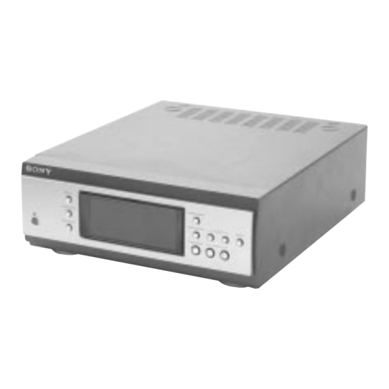
ST-S5 is the tuner section
in MHC-S7AV.
Sony Corporation
9-873-832-11
2001D0500-1
Home Audio Company
SPECIFICATIONS
Tuner section
FM stereo, FM/AM superheterodyne tuner
FM tuner section
Tuning range
87.5 – 108.0 MHz
Antenna
FM lead antenna
Antenna terminals
75 ohm unbalanced
Intermediate frequency
10.7 MHz
AM tuner section
Tuning range
AEP, UK models:
531 – 1,602 kHz
(with the interval set at
9 kHz)
Other models:
531 – 1,602 kHz
(with the interval set at
9 kHz)
530 – 1,710 kHz
(with the interval set at
10 kHz)
Antenna
AM loop antenna
Antenna terminals
External antenna terminal
Intermediate frequency
450 kHz
Approx. 280 x 108 x 340 mm
Dimensions (w/h/d)
Mass
Approx. 2.1 kg
Design and specifications are subject to change
without notice.
ST-S5
Australian Model
FM STEREO/FM-AM
SUPERHETERODYNE TUNER
AEP Model
UK Model
E Model
Advertisement
Table of Contents

Related Manuals for Sony ST-S5


Summary of Contents for Sony ST-S5
- Page 1 ST-S5 SERVICE MANUAL AEP Model UK Model Ver 1.0 2001.04 E Model Australian Model ST-S5 is the tuner section in MHC-S7AV. SPECIFICATIONS Tuner section FM stereo, FM/AM superheterodyne tuner FM tuner section Tuning range 87.5 – 108.0 MHz Antenna FM lead antenna...
-
Page 2: Table Of Contents
3-1. Disassembly Flow ............6 OPERATION. REPLACE THESE COMPONENTS WITH 3-2. Cover ................7 SONY PARTS WHOSE PART NUMBERS APPEAR AS 3-3. Front Panel Section ............7 SHOWN IN THIS MANUAL OR IN SUPPLEMENTS PUB- 3-4. PANEL Board, SIRCS Board ......... 8 LISHED BY SONY. -
Page 3: Servicing Notes
ST-S5 SECTION 1 SERVICING NOTES This set is a component of the MHC-S7AV. • MODEL IDENTIFICATION The MHC-S7AV system configuration is as shown below, and – Rear Panel – therefore it does not operate normally unless all four components are connected. -
Page 4: General
ST-S5 SECTION 2 This section is extracted from instruction manual. GENERAL LOCATION OF CONTROLS – Front Panel – qjqk ql w; CLOCK/TIMER wg (13, 21, 29) DISPLAY qh (13, 16, 18, 29, 35) ENTER w; (17, 18) IR receptor wh PRESET +/–... -
Page 5: Setting The Time
ST-S5 Setting the time Remote Control Turn on the system. Press CLOCK/TIMER (or CLOCK/TIMER 1 2 3 SET on the remote). When you set the time for the first time, proceed to step 5. Press O or o repeatedly to select “CLOCK SET”. -
Page 6: Disassembly
ST-S5 SECTION 3 DISASSEMBLY • This set can be disassembled in the order shown below. 3-1. DISASSEMBLY FLOW 3-2. COVER (Page 7) 3-3. FRONT PANEL SECTION 3-5. TUNER PACK (FM/AM) 3-7. DSP BOARD (Page 7) (Page 8) (Page 9) 3-4. PANEL BOARD, 3-6. -
Page 7: Cover
ST-S5 Note: Follow the disassembly procedure in the numerical order given. 3-2. COVER 3 cover 1 screw (+BVTT3 × 6 (S)) 2 two screws (case 3 TP2) 2 two screws (case 3 TP2) 3-3. FRONT PANEL SECTION 1 wire (flat type) (19 core) -
Page 8: Panel Board, Sircs Board
ST-S5 3-4. PANEL BOARD, SIRCS BOARD 2 two screws (BVTP2.6 × 8) 6 SIRCS board 4 PANEL board 2 four screws (BVTP2.6 × 8) 5 two claws 2 screw (BVTP2.6 × 8) (AEP, UK models) 1 wire (flat type) (19 core) -
Page 9: Main Board
ST-S5 3-6. MAIN BOARD 1 wire (flat type) (23 core) (CN508) 2 five connectors (CN510, 5031, 5032, 5041, 5042) 1 wire (flat type) (21 core) (CN509) 6 MAIN board 4 screw 4 two screws (BVTP3 × 8) (BVTP3 × 8) -
Page 10: Test Mode
SECTION 4 TEST MODE [GC Test Mode] Note: Use flowing buttons in the test mode. no mark : Button of tuner unit (ST-S5) Enter the GC Test Mode mode : Button of amplifier unit (TA-S7AV) Procedure 1: : Button of CD unit (CDP-S3) 1. -
Page 11: Diagrams
ST-S5 SECTION 5 DIAGRAMS 5-1. NOTE FOR PRINTED WIRING BOARDS AND SCHEMATIC DIAGRAMS • Circuit Boards Location Note on Printed Wiring Board: Note on Schematic Diagram: DSP board • All capacitors are in µF unless otherwise noted. pF: µµF • X : parts extracted from the component side. -
Page 12: Schematic Diagram - Main Board (1/2)
ST-S5 5-2. SCHEMATIC DIAGRAM – MAIN Board (1/2) – (1/2) CN5031 M(A)-GND EVER+5V D-GND NO901 NO991 C991 D+5V +15V REGULATOR (Page 13) IC991 C992 NJM7815FA CN5041 MIC-SIG MIC-GND (A-GND) FL-OUT FRONT-GND FR-OUT CENTER-OUT CENTER-GND (Page 13) SL-OUT S-GND SR-OUT OPTICAL RECEIVER... - Page 13 ST-S5 5-3. SCHEMATIC DIAGRAM – MAIN Board (2/2) – • See page 20 for Waveforms. (2/2) CN506 (AEP,UK) (E,AUS) ST-CLK (AEP,UK) R957 ST-DIN MC D0 ST-DOUT MC D1 COAXIAL ST-CE FM 75Ω A+10V R958 TUNED C962 R959 C961 FM/AM STEREO...
-
Page 14: Printed Wiring Board - Main Board
ST-S5 5-4. PRINTED WIRING BOARD – MAIN Board – • See page 11 for Circuit Boards Location. • Semiconductor Location Ref. No. Location ANTENNA D551 (E, AUS) D552 (AEP, UK) 75Ω D901 COAXIAL D902 SYSTEM FM 75Ω D903 CONTROL 1... -
Page 15: Printed Wiring Board - Dsp Board
ST-S5 5-5. PRINTED WIRING BOARD – DSP Board – • See page 11 for Circuit Boards Location. • Semiconductor Location Ref. No. Location J601 VIDEO D601 (AUDIO) D604 J602 D605 D607 WOOFER D608 IC609 DSP BOARD D609 OPTICAL (CONDUCTOR SIDE) -
Page 16: Schematic Diagram - Dsp Board (1/2)
ST-S5 5-6. SCHEMATIC DIAGRAM – DSP Board (1/2) – • See page 20 for Waveforms. • See page 20 for IC Block Diagram. C657 1000p C656 C655 R664 CN602 A+5V FB608 A-GND R680 FB607 DIGITAL 3.3k D+5V FILTER, D/A CONVERTER... -
Page 17: Schematic Diagram - Dsp Board (2/2)
ST-S5 5-7. SCHEMATIC DIAGRAM – DSP Board (2/2) – • See page 20 for Waveforms. • See page 20 for IC Block Diagram. Q603 Q603 2SC1623 REGULATOR R776 (E,AUS) R778 C690 C691 R777 R775 R762 FB606 INPUT SELECT SWITCH, C689... -
Page 18: Printed Wiring Boards - Panel Section
ST-S5 5-8. PRINTED WIRING BOARDS – PANEL Section – • See page 20 for Circuit Boards Location. PANEL BOARD C610 JW24 R603 FL601 JW11 C601 FLUORESCENT C653 C655 C657 C659 C661 C651 INDICATOR C649 TUBE C664 S611 C650 S601 SIRCS... -
Page 19: Schematic Diagram - Panel Section
ST-S5 5-9. SCHEMATIC DIAGRAM – PANEL Section – • See page 20 for Waveform. FL601 FLUORESCENT INDICATOR TUBE C610 (AEP,UK) R616 S612 100k CN602 R627 5.6k DISP/STANDBY KEY S611 D-GND STEREO/ MONO JOG2-B JOG2-A S610 R626 JOG1-B 3.9k TUNER MEMORY... - Page 20 ST-S5 • Waveforms • IC Block Diagrams – MAIN Board – – DSP Board – – DSP Board – 1 IC501 qa (XCOUT) 1 IC601 9 (MCLK1), IC604 w; (XMCK), 5 IC601 ws (KFSIO), IC604 qd (CKOUT) IC604 LC89056W-E wa (XOUT) 4.4 Vp-p...
-
Page 21: Ic Pin Function Description
ST-S5 5-10. IC PIN FUNCTION DESCRIPTION • MAIN BOARD IC501 M30622MGA-A39FP (SYSTEM CONTROLLER) Pin No. Pin Name Description AMP-DATA Serial data output to the M61512FP (IC607) AMP-CLK Serial data transfer clock signal output to the M61512FP (IC607) AMP-LAT Serial data latch pulse signal output to the M61512FP (IC607) - Page 22 ST-S5 Pin No. Pin Name Description — Ground terminal 65 to 70 — — Not used (open) LINE-MUTE Audio line muting on/off control signal output to the audio line circuit “L”: muting on — — Not used (open) DISPLAY KEY...
- Page 23 ST-S5 • DSP BOARD IC601 CXD9617R (AUDIO DIGITAL SIGNAL PROCESSOR) Pin No. Pin Name Description — Ground terminal XRST Reset signal input from the M61512FP (IC607) “L”: reset EXTIN Master clock signal input terminal Not used (fixed at “L”) Sampling frequency selection signal input terminal Not used (fixed at “L”) VDDI —...
- Page 24 ST-S5 Pin No. Pin Name Description — Ground terminal WMD0 S-RAM wait mode setting terminal Fixed at “L” in this set PAGE2 Page selection signal output terminal Not used (open) — Ground terminal PAGE1, PAGE0 52, 53 Page selection signal output terminal Not used (open) BOOT Boot mode control signal output terminal Not used (fixed at “L”)
- Page 25 ST-S5 • DSP BOARD IC604 LC89056W-E (DIGITAL AUDIO INTERFACE RECEIVER) Pin No. Pin Name Description DISEL Selection terminal of data input terminal Fixed at “L” in this set DOUT Digital data output to the optical transceiver (IC609) DIN0 Digital data input from the optical receiver (IC952) (for CDP-S3)
- Page 26 ST-S5 • DSP BOARD IC605 AK4527 (A/D, D/A CONVERTER) Pin No. Pin Name Description Audio serial data source selection signal input terminal SDOS “L”: internal ADC output, “H”: DAUX input (fixed at “L” in this set) Serial control mode selection signal input terminal “L”: 3-wire serial, “H”: I2C bus SMUTE Soft muting on/off signal input from the system controller (IC501) “L”: muting on...
- Page 27 ST-S5 • PANEL BOARD IC601 MB90M407PF-G-102-BND (DISPLAY CONTROLLER) Pin No. Pin Name Description 1 to 6 G6 to G1 Grid drive signal output to the fluorescent indicator tube (FL601) 7 to 10 A1 to A4 Segment drive signal output to the fluorescent indicator tube (FL601) VSS FOR IO —...
-
Page 28: Exploded Views
ST-S5 SECTION 6 EXPLODED VIEWS NOTE: • -XX and -X mean standardized parts, so they • Items marked “*” are not stocked since they may have some difference from the original are seldom required for routine service. Some one. delay should be anticipated when ordering •... -
Page 29: Chassis Section
ST-S5 6-2. CHASSIS SECTION (Including not supplied not supplied not supplied Ref. No. Part No. Description Remark Ref. No. Part No. Description Remark * 51 4-924-098-01 HOLDER, PC BOARD 4-232-327-01 PANEL (ST), BACK (AEP, UK) A-2007-939-A MAIN BOARD, COMPLETE (MX) -
Page 30: Electrical Parts List
ST-S5 SECTION 7 ELECTRICAL PARTS LIST NOTE: • Due to standardization, replacements in the • Items marked “*” are not stocked since they The components identified by mark 0 or dotted line with mark parts list may be different from the parts speci- are seldom required for routine service. - Page 31 ST-S5 Ref. No. Part No. Description Remark Ref. No. Part No. Description Remark C684 1-126-964-11 ELECT 10uF < DIODE/RESISTOR > C685 1-126-964-11 ELECT 10uF C686 1-126-933-11 ELECT 100uF D601 8-719-158-02 DIODE RD3.9SB2 C687 1-126-933-11 ELECT 100uF D604 8-719-988-61 DIODE 1SS355TE-17...
- Page 32 ST-S5 Ref. No. Part No. Description Remark Ref. No. Part No. Description Remark Q610 8-729-141-73 TRANSISTOR 2SC3624A-T1L15L16 R658 1-216-809-11 METAL CHIP 1/16W R659 1-216-809-11 METAL CHIP 1/16W Q611 8-729-141-73 TRANSISTOR 2SC3624A-T1L15L16 R660 1-216-815-11 METAL CHIP 1/16W Q612 8-729-113-69 TRANSISTOR FN1F4M-M32...
- Page 33 ST-S5 MAIN Ref. No. Part No. Description Remark Ref. No. Part No. Description Remark R723 1-216-821-11 METAL CHIP 1/16W A-2007-939-A MAIN BOARD, COMPLETE (MX) A-4476-193-A MAIN BOARD, COMPLETE (AEP, UK) R724 1-216-841-11 METAL CHIP 1/16W A-4476-203-A MAIN BOARD, COMPLETE (KR, AUS)
- Page 34 ST-S5 MAIN Ref. No. Part No. Description Remark Ref. No. Part No. Description Remark < CONNECTOR > Q902 8-729-011-92 TRANSISTOR 2SC2001TP-K1K2 CN502 1-784-780-11 CONNECTOR, FFC 19P < RESISTOR > * CN505 1-569-624-11 SOCKET, CONNECTOR 17P (SYSTEM CONTROL 3) R501 1-247-807-31 CARBON...
- Page 35 ST-S5 MAIN PANEL Ref. No. Part No. Description Remark Ref. No. Part No. Description Remark R549 1-247-843-11 CARBON 3.3K 1/4W C653 1-162-282-31 CERAMIC 100PF R550 1-249-441-11 CARBON 100K 1/4W C654 1-162-282-31 CERAMIC 100PF R551 1-249-413-11 CARBON 1/4W R552 1-249-429-11 CARBON...
- Page 36 ST-S5 PANEL SIRCS Ref. No. Part No. Description Remark Ref. No. Part No. Description Remark R633 1-249-417-11 CARBON 1/4W R634 1-249-429-11 CARBON 1/4W R635 1-249-417-11 CARBON 1/4W R636 1-249-429-11 CARBON 1/4W R637 1-249-417-11 CARBON 1/4W R638 1-249-429-11 CARBON 1/4W R639...
- Page 37 ST-S5 MEMO...
- Page 38 ST-S5 REVISION HISTORY Clicking the version allows you to jump to the revised page. Also, clicking the version at the upper right on the revised page allows you to jump to the next revised page. Ver. Date Description of Revision...
Need help?
Do you have a question about the ST-S5 and is the answer not in the manual?
Questions and answers