Table of Contents
Advertisement
Quick Links
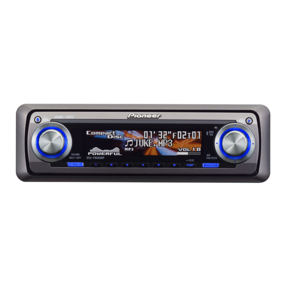
MULTI-CD CONTROL DSP HIGH POWER CD/MP3/WMA PLAYER WITH FM/AM TUNER
DEH-P860MP
DEH-P8600MP
DEH-P8650MP
This service manual should be used together with the following manual(s):
Model No.
Order No.
CX-3098
CRT3179
For details, refer to "Important symbols for good services".
PIONEER CORPORATION
PIONEER ELECTRONICS (USA) INC. P.O. Box 1760, Long Beach, CA 90801-1760, U.S.A.
PIONEER EUROPE NV Haven 1087, Keetberglaan 1, 9120 Melsele, Belgium
PIONEER ELECTRONICS ASIACENTRE PTE. LTD. 253 Alexandra Road, #04-01, Singapore 159936
PIONEER CORPORATION 2004
Mech.Module
S10WMAcode2
CD Mech. Module:Circuit Description, Mech. Description, Disassembly
4-1, Meguro 1-chome, Meguro-ku, Tokyo 153-8654, Japan
DEH-P860MP/XN/UC
/XN/UC
/XN/ES
Remarks
ORDER NO.
CRT3217
/XN/UC
K-ZZD.MAR. 2004 printed in Japan
Advertisement
Table of Contents

Related Manuals for Pioneer DEH-P860XN


Summary of Contents for Pioneer DEH-P860XN
- Page 1 PIONEER CORPORATION 4-1, Meguro 1-chome, Meguro-ku, Tokyo 153-8654, Japan PIONEER ELECTRONICS (USA) INC. P.O. Box 1760, Long Beach, CA 90801-1760, U.S.A. PIONEER EUROPE NV Haven 1087, Keetberglaan 1, 9120 Melsele, Belgium PIONEER ELECTRONICS ASIACENTRE PTE. LTD. 253 Alexandra Road, #04-01, Singapore 159936 PIONEER CORPORATION 2004 K-ZZD.MAR.
-
Page 2: Safety Information
SAFETY INFORMATION CAUTION This service manual is intended for qualified service technicians; it is not meant for the casual do-it-yourselfer. Qualified technicians have the necessary test equipment and tools, and have been trained to properly and safely repair complex products such as those covered by this manual. Improperly performed repairs can adversely affect the safety and reliability of the product and may void the warranty. - Page 3 [ Important symbols for good services ] In this manual, the symbols shown-below indicate that adjustments, settings or cleaning should be made securely. When you find the procedures bearing any of the symbols, be sure to fulfill them: 1. Product safety You should conform to the regulations governing the product (safety, radio and noise, and other regulations), and should keep the safety during servicing by following the safety instructions described in this manual.
-
Page 4: Table Of Contents
CONTENTS SAFETY INFORMATION ............................. 2 1. SPECIFICATIONS ............................5 2. EXPLODED VIEWS AND PARTS LIST ......................8 2.1 PACKING(DEH-P860MP/XN/UC,DEH-P8600MP/XN/UC)................. 8 2.2 PACKING(DEH-P8650MP/XN/ES)......................10 2.3 EXTERIOR(1) ............................12 2.4 EXTERIOR(2) ............................14 2.5 CD MECHANISM MODULE........................16 3. BLOCK DIAGRAM AND SCHEMATIC DIAGRAM ..................18 3.1 BLOCK DIAGRAM ........................... -
Page 5: Specifications
1. SPECIFICATIONS DEH-P860MP/XN/UC... - Page 6 DEH-P860MP/XN/UC...
- Page 7 DEH-P860MP/XN/UC...
-
Page 8: Exploded Views And Parts List
2. EXPLODED VIEWS AND PARTS LIST OTES : • Parts marked by " * " are generally unavailable because they are not in our Master Spare Parts List. • Screw adjacent to mark on the product are used for disassembly. •... - Page 9 (1) PACKING(DEH-P860MP/XN/UC,DEH-P8600MP/XN/UC) SECTION PARTS LIST Mark No. Description Part No. Mark No. Description Part No. 17-2 Owner's Manual See Contrast table(2) Cord Assy See Contrast table(2) 17-3 Installation Manual See Contrast table(2) Cord Assy CDE7701 17-4 Causion Card CRP1308 Accessory Assy CEA4302 Spring CBH1650...
-
Page 10: Packing(Deh-P8650Mp/Xn/Es)
2.2 PACKING(DEH-P8650MP/XN/ES) DEH-P860MP/XN/UC... - Page 11 - - - - PACKING(DEH-P8650MP/XN/ES) SECTION PARTS LIST Mark No. Description Part No. Mark No. Description Part No. 17-2 Owner's Manual CRD3832 Cord Assy CDE7436 17-3 Owner's Manual CRD3833 Cord Assy CDE7701 17-4 Owner's Manual CRB1902 Accessory Assy CEA4301 Spring CBH1650 17-5 Installation Manual CRD3834...
-
Page 12: Exterior(1)
2.3 EXTERIOR(1) (2/2) (2/2) : GEM1024 DEH-P860MP/XN/UC... - Page 13 (1) EXTERIOR(1) SECTION PARTS LIST Mark No. Description Part No. Mark No. Description Part No. Screw(M2x2.5) CBA1641 Holder CND2039 Screw(M2.6x4) CBA1769 CNV6963 Drive Unit See Contrast table(2) Lighting Conductor CNV7974 Screw BMZ26P040FTC Lighting Conductor CNV7975 Screw CBA1633 Keyboard Unit CWM9270 Spring CBL1632 Flat Cable...
-
Page 14: Exterior(2)
2.4 EXTERIOR(2) (1/2) (1/2) DEH-P860MP/XN/UC... - Page 15 (1) EXTERIOR(2) SECTION PARTS LIST Mark No. Description Part No. Mark No. Description Part No. Connector(CN351) CKM1389 Screw BMZ26P060FZK Screw BSZ26P060FTC Plug(CN571) CKS-786 Screw(M2.6x14) CBA1632 ••••• IC(IC301) PAL007A Connector(CN702) CKS3126 Transistor(Q742,861,871) 2SD2396 Connector(CN101) CKS3408 Connector(CN701) CKS3837 Cord Assy CDE7701 Fuse(10A) CEK1136 Connector(CN931) See Contrast table(2)
-
Page 16: Cd Mechanism Module
2.5 CD MECHANISM MODULE 1GEM1024 2GEM1045 3GEM1035 DEH-P860MP/XN/UC... - Page 17 Mark No. Description Part No. Mark No. Description Part No. CD Core Unit(S10WMACODE2) CWX2953 Gear CNV7208 Connector(CN101) CKS4182 Gear CNV7209 Connector(CN901) CKS4017 Gear CNV7210 Screw BMZ20P035FTC Gear CNV7211 Screw BSZ20P040FTC Gear CNV7212 Screw(M2x4) CBA1362 Rack CNV7214 Screw(M2x3) CBA1511 CNV7215 Screw(M2x3) CBA1527 CNV7216 •••••...
-
Page 18: Block Diagram And Schematic Diagram
3. BLOCK DIAGRAM AND SCHEMATIC DIAGRAM 3.1 BLOCK DIAGRAM CN101 TUNER AMP UNIT BUS+L 10 9 8 18 19 20 21 BUS-L FM/AM TUNER UNIT IC 5 IC 3 EEPROM 3.3V 5.0V ANTENNA CN402 AM ANT FMRF IC 2 IC 1 2.5V 3.3V FM ANT... - Page 19 CN351 RESET MUTE CN101 WOOFER L Q651 Q101 IC 651 Q352 B.UP S-80835CNMC-B8U RST1 BZ601 BUZZER ASENBO IC 321 REAR L PEE 22 PA2028A IP-BUS DRIVER Q353 BUS- IC 101 HA12240FP SYSTEM CONTROLLER BUS+ MODE S551 FRONT L IPPW IPPW MUTE Q351 Q354...
-
Page 20: Overall Connection Diagram(Guide Page)
3.2 OVERALL CONNECTION DIAGRAM(GUIDE PAGE) Note: When ordering service parts, be sure to refer to " EXPLODED VIEWS AND PARTS LIST" or "ELECTRICAL PARTS LIST". Large size SCH diagram TUNER AMP UNIT Guide page : SIGNAL LINE : POWER SUPPLY LINE 2.5V Detailed page 2.5V... - Page 21 NOTE : Symbol indicates a resistor. Decimal points for resistor 3.3V No differentiation is made between chip resistors and 4.7V and capacitor fixed values discrete resistors. are expressed as : 4.7V ← Symbol indicates a capacitor. ← No differentiation is made between chip capacitors and 0.022 R022 5.0V...
- Page 22 DEH-P860MP/XN/UC...
- Page 23 DEH-P860MP/XN/UC...
- Page 24 DEH-P860MP/XN/UC...
- Page 25 DEH-P860MP/XN/UC...
-
Page 26: Keyboard Unit
3.3 KEYBOARD UNIT REMOTE CONTROL SENSOR RESET MICROPHONE INPUT 5.2V 9.9V 9.1V MULTI-CONTROL OPEN DISP SOURCE/VOLUME CLOCK BAND/ESC DEH-P860MP/XN/UC... - Page 27 KEYBOARD UNIT FONT ROM OEL CONTROL/ KEY CONTROL OEL MODULE MXK8200 DEH-P860MP/XN/UC...
-
Page 28: Cd Mechanism Module(Guide Page)
3.4 CD MECHANISM MODULE(GUIDE PAGE) L209 C217 PICKUP UNIT(P9.9MP3)(SERVICE) Pull-down CXB6007 SPINDLE MOTOR CXB8933 LOADING/CARRIAGE CD DRIVER MOTOR 3.3V REGULATOR DEH-P860MP/XN/UC... - Page 29 CD CORE UNIT(S10WMACODE2) SWITCHES: CD CORE UNIT(S10WMACODE2) S901 : HOME SWITCH..ON-OFF S902 : CLAMP SWITCH..ON-OFF S903 : DSCSNS SWITCH..ON-OFF S904 : 12EJ SWITCH....ON-OFF S905 : 8EJ SWITCH....ON-OFF The underlined indicates the switch position. 1.5V REGULATOR SIGNAL LINE FOCUS SERVO LINE TRACKING SERVO LINE CARRIAGE SERVO LINE SPINDLE SERVO LINE...
- Page 30 DEH-P860MP/XN/UC...
- Page 31 4.00MHz DEH-P860MP/XN/UC...
- Page 32 DEH-P860MP/XN/UC...
- Page 33 DEH-P860MP/XN/UC...
- Page 34 - Waveforms Note : 1. The encircled numbers denote measuring points in the circuit diagram. 2. Reference voltage REFO1(1.65V) 1 DSCSNS 1 DSCSNS 1 DSCSNS 5V/div 500ms/div 5V/div 500ms/div 5V/div 500ms/div 2 8SNS 5 CLCONT 2 8SNS 5V/div 5V/div 5V/div 3 12SNS 4 LOEJ 3 12SNS...
- Page 35 0 FIN @ TE % RFAGC 500mV/div 200ms/div 500mV/div 2ms/div 1V/div 500µs/div # FE % RFAGC @ TE 500mV/div 500mV/div 500mV/div 9 TIN 500mV/div Focus Search waveform Track Open waveform 1 Track Jump waveform Ref.: Ref.: Ref.: REFO REFO REFO Mode: Mode: Mode:...
- Page 36 ^ LRCK ^ LRCK ^ LRCK 2V/div 5µs/div 1V/div 1µs/div 1V/div 1µs/div & BCK & BCK * DOUT 2V/div 1V/div 1V/div * DOUT 2V/div Digtal audio waveform Digtal audio waveform Analog audio waveform Ref.: Ref.: Ref.: AGND Mode: Mode: Mode: Normal Normal Normal...
- Page 37 DEH-P860MP/XN/UC...
-
Page 38: Pcb Connection Diagram
4. PCB CONNECTION DIAGRAM 4.1 TUNER AMP UNIT NOTE FOR PCB DIAGRAMS CORD ASSY TUNER AMP UNIT 1.The parts mounted on this PCB (POWER SUPPLY, SPEAKER) include all necessary parts for several destination. For further information for WIRED REMOTE respective destinations, be sure CONTROL to check with the schematic dia- gram. - Page 39 SIDE A CORD ASSY(RCA OUT) ANTENNA CABLE IC,Q IP-BUS CN902 CN901 M571 FLAP MOTOR FRONT DEH-P860MP/XN/UC...
- Page 40 TUNER AMP UNIT IC,Q TEST DEH-P860MP/XN/UC...
- Page 41 SIDE B DEH-P860MP/XN/UC...
-
Page 42: Switch Unit
4.2 SWITCH UNIT SWITCH UNIT CN571 CLOSE OPEN DEH-P860MP/XN/UC... -
Page 43: Keyboard Unit
4.3 KEYBOARD UNIT SIDE B SIDE A KEYBOARD UNIT KEYBOARD UNIT IC,Q IC,Q MODULE CN801 DEH-P860MP/XN/UC... -
Page 44: Cd Mechanism Module
4.4 CD MECHANISM MODULE SIDE A CD CORE UNIT(S10WMACODE2) LOADING /CARRIAGE MOTOR SPINDLE MOTOR CN701 HOME CN702 DEH-P860MP/XN/UC... - Page 45 SIDE B CD CORE UNIT(S10WMACODE2) 12EJ DSCSNS CLAMP DEH-P860MP/XN/UC...
-
Page 46: Electrical Parts List
5. ELECTRICAL PARTS LIST Circuit Symbol and No. Part No. Circuit Symbol and No. Part No. Q 561 Transistor 2SD1859 Q 562 Transistor IMD2A Q 571 Transistor 2SD1760F5 Q 572 Transistor IMD3A Q 651 Transistor 2SC3052-12 Unit Number:CWM9266(P860MP) Unit Number:CWM9267(P8600MP) Q 741 Transistor IMD2A... - Page 47 Circuit Symbol and No. Part No. Circuit Symbol and No. Part No. D 741 Diode HZS9L(B1) BZ601 Buzzer CPV1062 D 742 Diode HZS6L(C1) Y 401 FM/AM Tuner Unit CWE1646 D 801 Diode Network DA204U D 802 Diode Network DA204U RESISTORS D 803 Diode Network DA204U...
- Page 48 Circuit Symbol and No. Part No. Circuit Symbol and No. Part No. R 234 RN1/16SE1502D R 402 RS1/16S681J R 261 RN1/16SE3300D R 403 RS1/16S681J R 262 RN1/16SE3300D R 404 RS1/16S681J R 263 RN1/16SE3300D R 405 RS1/16S681J R 264 RN1/16SE3300D R 406 RS1/16S681J R 265 RN1/16SE4702D...
- Page 49 Circuit Symbol and No. Part No. Circuit Symbol and No. Part No. R 642 RS1/16S104J R 881 RS1/16S333J R 651 RS1/16S102J R 882 RS1/16S821J R 652 RS1/16S222J R 883 RS1/16S821J R 653 RS1/16S102J R 891 RS1/16S103J R 654 RS1/16S473J R 892 RS1/16S104J R 655 RS1/16S183J...
- Page 50 Circuit Symbol and No. Part No. Circuit Symbol and No. Part No. C 193 CCSRCH102J50 C 294 CKSRYB104K16 C 194 CKSYB106K6R3 C 301 CFTNA224J50 C 196 CCSRCH102J50 C 302 CFTNA224J50 C 197 CKSYB106K6R3 C 303 CFTNA224J50 C 199 CKSYB106K6R3 C 304 CFTNA224J50 C 200 CCSRCH102J50...
- Page 51 Circuit Symbol and No. Part No. Circuit Symbol and No. Part No. C 525 CKSRYB474K10 C 948 CKSRYB104K16 C 526 CKSRYB104K16 C 949 CKSYB475K10 C 527 CCSRCH101J50 C 961 CEAL470M6R3 C 528 CKSRYB105K10 C 962 CKSRYB104K16 C 529 CEAL100M16 C 964 CKSRYB104K16 C 530 CKSRYB105K10...
- Page 52 Circuit Symbol and No. Part No. Circuit Symbol and No. Part No. S 1909 Push Switch CSG1155 R 1919 RS1/16S221J R 1921 RS1/16S221J S 1910 Push Switch CSG1155 R 1923 RS1/16S221J S 1911 Push Switch CSG1155 R 1925 RS1/16S221J S 1912 Encoder(SOURCE/VOLUME)CSD1104 R 1927 RS1/16S821J...
- Page 53 Circuit Symbol and No. Part No. Circuit Symbol and No. Part No. IC 301 BA5835FM R 261 RS1/16S0R0J IC 501 S-L2980A15MC-C6A R 262 RS1/16S0R0J IC 701 PE5423A R 263 RS1/16S0R0J IC 703 S-812C33AUA-C2N R 264 RS1/16S0R0J Q 101 Transistor 2SB1132 R 267 RS1/16S0R0J Q 701...
- Page 54 Circuit Symbol and No. Part No. Circuit Symbol and No. Part No. R 778 RS1/16SS221J R 779 RS1/16SS221J C 505 CKSQYB475K6R3 R 901 RAB4CQ221J C 701 CKSSYB104K10 C 702 CKSSYB471K50 R 902 RS1/16S0R0J C 703 CKSSYB103K16 R 905 RS1/16SS221J C 704 4.7µF/25V CCH1592 R 906...
-
Page 55: Adjustment
6. ADJUSTMENT 6.1 JIG CONNECTION DIAGRAM TUNER AMP UNIT CN801 GGD1160 GGD1378 KEYBOARD UNIT CN1903 Rubber Band Rubber Band DEH-P860MP/XN/UC... -
Page 56: Cd Adjustment
6.2 CD ADJUSTMENT 1) Cautions on adjustments 2) Test mode • In this product the single voltage (3.3V) is used for the This mode is used to adjust the CD mechanism module. regulator. The reference voltage is the REFO1 (1.65V) •... - Page 57 - Flow Chart [4]+[6]+Reset or [KEY] [4]+[6]+BU+ACC Contents Test Mode In Display [CD]or[SOURCE] Source On [BAND] Power On Power On RF AMP SPINDLE (T.Offset is adjusted) (T.Offset is not adjusted) Gain switching Speed switching [→] [←] [BAND] Tracking Servo Focus Close Focus Mode Automatic adjustment CRG+...
-
Page 58: Checking The Grating After Changing The Pickup Unit
6.3 CHECKING THE GRATING AFTER CHANGING THE PICKUP UNIT • Note : The grating angle of the PU unit cannot be adjusted after the PU unit is changed. The PU unit in the CD mechanism module is adjusted on the production line to match the CD mechanism module and is thus the best adjusted PU unit for the CD mechanism module. - Page 59 Ech → Xch 20mV/div, AC Grating waveform Fch → Ych 20mV/div, AC 0° 30° 45° 60° 75° 90° DEH-P860MP/XN/UC...
-
Page 60: Error Mode
6.4 ERROR MODE - Error Messages If a CD is not operative or stopped during operation due to an error, the error mode is turned on and cause(s) of the error is indicated with a corresponding number. This arrangement is intended at reducing nonsense calls from the users and also for facilitating trouble analysis and repair work in servicing. -
Page 61: Oel Screensaver Studio Lka To Lkd Application
CD-R disc and install it to car audio. This function is similar to PC link-kit (CD-PC1). "OEL Screensaver Studio" is available to the public on the PIONEER Home Page. This software (GGV1168) is added LKA to LKD file conversion function to original "OEL Screensaver Studio". -
Page 62: General Information
7. GENERAL INFORMATION 7.1 DIAGNOSIS 7.1.1 DISASSEMBLY - Removing the Case (not shown) 1. Remove the two screws and then remove the Case. CD Mechanism Module - Removing the CD Mechanism Module (Fig.1) Remove the four screws. Disconnect the connector and then remove the CD Mechanism Module. - Page 63 - Removing the Tuner Amp Unit (Fig.3) Remove the three screws. Remove the screw. Straighten the tabs at three locations indicated. Remove the screw and then remove the Tuner Amp Unit. Tuner Amp Unit Fig.3 - Notes when assembling (Fig.4) The Holder hook touches the Sub Grille Assy.
- Page 64 - How to hold the Mechanism Unit 1. Hold the top and bottom frame. 2. Do not squeeze top frame's front portion too tight, because it is fragile. Do not squeeze. - Removing the Upper and Lower Frames 1. With a disc clamped, remove the four springs (A), Upper Frame the two springs (B), the two springs (C), and the four screws.
- Page 65 - Removing the Pickup Unit 1. Apply shorting solder to the Pickup flexible cable. Disconnect the cable. 2. Set the mechanism to the clamp mode. 3. Remove the lead wires from the inner holder. 4. Remove the washer, styling holder, change arm, and pickup lock arm.
-
Page 66: Connector Function Description
7.1.2 CONNECTOR FUNCTION DESCRIPTION DEH-P860MP/XN/UC... - Page 67 7.2 IC PD5928A NJM2872F05 PE5423A NJM4580V AK7730VT UPD63761GJ PCM1742KE PD5943A S-812C33AUA-C2N HA12240FP PD8126A BA5835FM NJM2112V TC7WH32FK S-L2980A15MC-C6A S-80835CNMC-B8U PD6468A - Pin Functions(PD5928A) Pin No. Pin Name Function and Operation SYSPW System power control output DSPPW DSP : Power control output DSPOUT DSP : Data output DSPIN...
- Page 68 Pin No. Pin Name Function and Operation FLPPW Flap motor driver power ON/OFF output Not used DSPCS DSP : Interface chip select output DSPRQ DSP : Interface request output DSPRDY DSP : Data write ready signal input DSPDRDY DSP : Data read ready signal input Power supply input EVOLCS Electronic volume chip select output...
- Page 69 PCM1742KE Audio Seria DATA Portl Output Amp and LRCK Low-Pass Filter 4x/8x Oversampling Enhanced DGND Digital Filter Multilevel with Delta-Sigma Function Modulator Serial Controller Control ZEROL/NA Port Output Amp and Low-Pass Filter ZEROR/ZEROA System Clock Zero Detect System Clock Manager AGND HA12240FP BUS+...
- Page 70 - Pin Functions(AK7730VT) Pin No. Pin Name Function and Operation EESEL Control Mode select pin (Pull down) JX0/SDIN4A External conditional jump pin / DSP serial data input pin (Pull down) 3, 4 SDIN3, 2/JX1, 2 DSP serial data input pin / External condition jump pin (Pull down) SDIN1 DSP serial data input pin (Pull down) CKS1...
- Page 71 NJM2112V NJM2872F05 NOISE VOUT BYPASS Thermal Protection Bandgap Reference CONTROL *S-80835CNMC-B8U VREF DEH-P860MP/XN/UC...
- Page 72 - Pin Functions (PD5943A) Pin No. Pin Name Format Function and Operation romcs Not used OPEN flstby Not used OPEN FL120N Not used OPEN flbusy Flash memory busy input Remote control reception input BYTE GND connection CNVSS GND connection 8, 9 Not used OPEN reset Pull up...
- Page 73 * PD5943A Format Meaning CMOS Nch open drain * PD8124A * TC7WH32FK 8 VCC 1A 1 7 1Y 1B 2 A0-A20 :Address input D0-D15 :Data output BYTE :Bank address BYTE :Chip enable input :Output enable input 6 2B AVCC :Power supply 2Y 3 :GND GND 4...
- Page 74 * PD6468A byte DQ15/A1 DQ14 DQ13 DQ12 A0-A17 : Address input DQ0-DQ15 : Data output : Chip enable input : Output enable input reset : Write enable input RY/by : Ready / Busy output DQ11 DQ10 RY/by DEH-P860MP/XN/UC...
- Page 75 - Pin Functions(PE5423A) Pin No. Pin Name Format Function and Operation AVREF A power supply Positive power supply(5V) AVSS A power supply GND RFOK Output of state of RFOK CLAMP CLAMP SW sense input EVDD E power supply Positive power supply For changer(PWM) Not used IC/FLMD0...
- Page 76 Pin No. Pin Name Format Function and Operation Not used xread CD LSI read control signal output XASTB CD LSI address strobe output BVSS B power supply GND BVDD B power supply Positive power supply 71-86 AD0-15 Address/data Bus 0-15 87-90 Not used 91-93...
- Page 77 - Pin Functions(UPD63761GJ) Pin No. Pin Name Function and Operation D.VDD Power supply for digital circuits D1.GND GND for 1.6V digital circuits reset Input of reset AB12-8 Address bus 12-8 from the microcomputer 9-16 AD7-0 Address/data bus 7-0 to the microcomputer Chip selection ASTB Address strobe...
- Page 78 Pin No. Pin Name Function and Operation D.VDD Power supply for digital circuits Output of focus drive PWM + Output of focus drive PWM - Output of tracking drive PWM + Output of tracking drive PWM - Output of thread drive PWM + Output of thread drive PWM - Output of spindle drive PWM + Output of spindle drive PWM -...
- Page 79 - Pin Functions(BA5835FM) Pin No. Pin Name Function and Operation Input pin for reference voltage OPIN2(+) Input pin for non-inverting input for CH2 preamplifier OPIN2(-) Input pin for inverting input for CH2 preamplifier OPOUT2 Output pin for CH2 preamplifier OPIN1(+) Input pin for non-inverting input for CH1 preamplifier OPIN1(-) Input pin for inverting input from CH1 preamplifier...
- Page 80 - FM/AM Tuner Unit 10 9 8 18 19 20 21 IC 5 IC 3 EEPROM 3.3V 5.0V AM ANT FMRF IC 2 2.5V IC 1 FM ANT 3.3V FMRF MIXER, IF AMP DET, FM MPX RF adj ANT adj CF52 CF51 IC 4...
-
Page 81: Operational Flow Chart
7.3 OPERATIONAL FLOW CHART Power ON VCC=5V Pin 14,60 bsens Pin 73 bsens=L asens Pin 72 asens=L dsens Pin 91 1.5V < DSENS < 4.5V ASENBO←H Pin 80 Starts communication with Grille microcomputer. 300ms SWVDD←H Pin 38 300ms In case of the above signal, the communication with Grille microcomputer may fail. -
Page 82: Cleaning
7.4 CLEANING Before shipping out the product, be sure to clean the following portions by using the prescribed cleaning tools: Portions to be cleaned Cleaning tools CD pickup lenses Cleaning liquid : GEM1004 Cleaning paper : GED-008 Portions to be cleaned Cleaning tools Fans Cleaning paper : GED-008... -
Page 83: Operations
8. OPERATIONS DEH-P860MP/XN/UC... - Page 84 DEH-P860MP/XN/UC...
- Page 85 DEH-P860MP/XN/UC...
- Page 86 - CONNECTION DIAGRAM(DEH-P860MP/XN/UC) DEH-P860MP/XN/UC...
- Page 87 - CONNECTION DIAGRAM(DEH-P8600MP/XN/UC) DEH-P860MP/XN/UC...
- Page 88 - CONNECTION DIAGRAM(DEH-P8650MP/XN/ES) DEH-P860MP/XN/UC...
- Page 89 DEH-P860MP/XN/UC...
- Page 90 - Jigs List Name Jig No. Remarks Test Disc TCD-782 Checking the grating L.P.F. Checking the grating g (Two pieces) Extension Cable GGD1160 Checking the keyboard unit Extension PCB GGD1378 Checking the keyboard unit CD-ROM GGV1168 OEL screensaver studio lka to lkd application Cleaning liquid GEM1004 Cleaning CD pickup lenses...
Need help?
Do you have a question about the DEH-P860XN and is the answer not in the manual?
Questions and answers