Table of Contents

Advertisement

HCD-GZR888D/GZR999D
SERVICE MANUAL
Ver. 1.2 2010.09
• HCD-GZR888D/GZR999D are the tuner,
deck, DVD and amplifi er section in MHC-
GZR888D/GZR999D.
Amplifi er section
The following measured at AC 127 V, 60 Hz
(Mexican model)
The following measured at AC 127 V, 220 V,
240 V, 50/60 Hz (Saudi Arabian model)
The following measured at AC 120 V, 220 V,
240 V, 50/60 Hz (Other models)
MHC-GZR999D
Power output (rated):
135 W + 135 W (at 6 Ω, 1 kHz, 1%
THD, at LINK MODE)
RMS output power (reference)
Front speaker:
210 W + 210 W (per channel at 8 Ω,
1 kHz)
Satellite speaker:
90 W + 90 W (per channel at 24 Ω,
1 kHz)
Subwoofer:
240 W (at 6 Ω, 100 Hz)
9-889-869-03
Sony Corporation
2010I04-1
©
2010.09
Published by Sony Techno Create Corporation
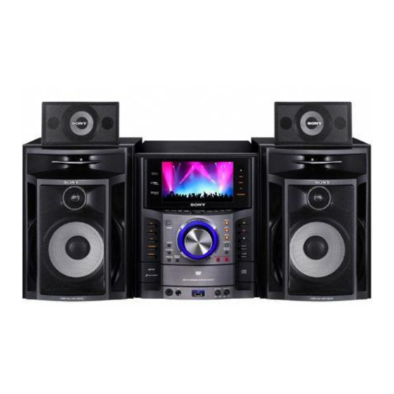
Photo: HCD-GZR999D: E3 model
Model Name Using Similar Mechanism
DVD
DVD Mechanism Type
Section
Optical Pick-up Name
Model Name Using Similar Mechanism
Tape Deck
Section
Tape Transport Mechanism Type
SPECIFICATIONS
MHC-GZR888D
Power output (rated):
125 W + 125 W (at 6 Ω, 1 kHz, 1%
THD, at LINK MODE)
RMS output power (reference)
Front speaker:
210 W + 210 W (per channel at 8 Ω,
1 kHz)
Satellite speaker:
90 W + 90 W (per channel at 24 Ω,
1 kHz)
HCD-GZR888D/GZR999D: E3, E4, E15, EA, PH, SP Model
E Model
HCD-GZR777D
CDM74HFVX-DVBU101
KHM-313CAB
HCD-GZR777D
CFP42608
– Continued on next page –
DVD DECK RECEIVER
HCD-GZR999D: E2, E51, AR, MX Model
DVD RECEIVER

Advertisement

Table of Contents
loading

Summary of Contents for Sony HCD-GZR888D

  • Page 1 90 W + 90 W (per channel at 24 Ω, 1 kHz) Subwoofer: 240 W (at 6 Ω, 100 Hz) HCD-GZR888D/GZR999D: E3, E4, E15, EA, PH, SP Model DVD DECK RECEIVER HCD-GZR999D: E2, E51, AR, MX Model DVD RECEIVER 9-889-869-03...
  • Page 2 COMPONENTS IDENTIFIED BY MARK 0 OR DOTTED LINE WITH MARK 0 ON THE SCHEMATIC DIAGRAMS AND IN THE PARTS LIST ARE CRITICAL TO SAFE OPERATION. REPLACE THESE COMPONENTS WITH SONY PARTS WHOSE PART NUMBERS APPEAR AS SHOWN IN THIS MANUAL OR IN SUPPLEMENTS PUBLISHED BY SONY.
  • Page 3 HCD-GZR888D/GZR999D NOTES ON CHIP COMPONENT REPLACEMENT NOTES ON LASER DIODE EMISSION CHECK • Never reuse a disconnected chip component. The laser beam on this model is concentrated so as to be focused • Notice that the minus side of a tantalum capacitor may be dam- on the disc reflective surface by the objective lens in the optical aged by heat.
  • Page 4 HCD-GZR888D/GZR999D Ver. 1.1 MODEL IDENTIFICATION – Back Panel – Parts No. Model Part No. GZR888D: E3 model 4-170-040-0[] GZR888D: E4 model 4-170-040-1[] GZR888D: EA model 4-170-040-2[] GZR888D: E12 model 4-170-040-3[] GZR888D: E15 model 4-170-040-4[] GZR888D: SP model 4-170-040-5[] GZR888D: TH model...
  • Page 5: Table Of Contents

    HCD-GZR888D/GZR999D TABLE OF CONTENTS SERVICING NOTES 6-7. Schematic Diagram –Driver Section– ......38 ..........6-8. Printed Wiring Board –DMB19 Board (1/2)– ....39 6-9. Printed Wiring Board –DMB19 Board (2/2)– ....40 DISASSEMBLY 6-10. Schematic Diagram –DMB19 Board (1/4)– ....41 2-1.
  • Page 6: Servicing Notes

    HCD-GZR888D/GZR999D SECTION 1 SERVICING NOTES Notes on Disconnecting Between the OP Section (DVBU101) and the DMB19 Board Note: When disconnecting between the OP section (DVBU101) and the DMB19 board, be sure to make a solder brige for electrostatic prevention as illus- trated in the figure (before disconnection). On the contrary, when installing the OP section, never remove the solder bride until the OP section and the DMB19 board are connected. Be sure to remove the solder bridge after the OP section and the DMB19 board have been connected. Perform solder bridging to prevent damage by electrostatic discharge when handling the BU as a single unit. Manual Opening and Closing the DVD Tray As illustrated, insert a flathead screwdriver and give a turn to the left to put the DVD tray out.
  • Page 7 HCD-GZR888D/GZR999D Ver. 1.2 Service Position for the BU DMB19 board Note for Replacement of the KNOB (JOG) When replacing the KNOB (JOG), apply the SANKOL FTA-001HA (Part No. J-2501-264-A) to the end of the rib at 6 places. SANKOL FTA-001HA...
  • Page 8: Disassembly

    HCD-GZR888D/GZR999D SECTION 2 DISASSEMBLY • This set can be disassembled in the order shown below. 2-1. CASE (SIDE-L), 2-21. CHASSIS CASE (SIDE-R) (Page 9) (Page 19) EXCEPT E2, E51, AR, MX MODEL 2-2. TOP PANEL SECTION 2-14. TC-AMP BOARD 2-22. DMB19 BOARD (Page 9) (Page 15) (Page 19) 2-3.
  • Page 9: Case (Side-L), Case (Side-R)

    HCD-GZR888D/GZR999D Note: Follow the disassembly procedure in the numerical order shown below. 2-1. CASE (SIDE-L), CASE (SIDE-R) 2 three screws 5 case (side-L) (+BVTP 3 × 8) 0 case (side-R) 1 three screws (case M 3 × 6) 7 three screws (+BVTP 3 × 8) 6 three screws (case M 3 × 6) 2-2.
  • Page 10: Loading Panel

    HCD-GZR888D/GZR999D 2-3. LOADING PANEL 3 loading panel flathead screwdriver As illustrated, insert a flathead screwdriver and give a turn to the left to DVD tray put the DVD tray out. 2-4. CHASSIS 6 CN1105 (4P) 1 screw (+BVTP 3 × 8) 2 two screws (+BVTP 3 ×...
  • Page 11: Front Panel Section

    HCD-GZR888D/GZR999D 2-5. FRONT PANEL SECTION 3 wire (flat type) (5 core) (CN101) 4 CN407 (4P) 6 screw (+BVTP 3 × 8) 2 wire (flat type) (21 core) (CN501) 7 lug 9 screw (+BVTP 3 × 8) 1 wire (flat type) (7 core) (CN503)
  • Page 12: Main Board

    HCD-GZR888D/GZR999D 2-7. MAIN BOARD 6 wire (flat type) (13 core) (CN641) 3 wire (flat type) (9 core) (CN211) 4 wire (flat type) (7 core) (CN191) 5 wire (flat type) (9 core) (CN504) 8 MAIN board 7 CN951 (9P) 1 two screws (+BVTP 3 ×...
  • Page 13: Dvd Mechanism Deck, Tuner (Tm901)

    HCD-GZR888D/GZR999D 2-9. DVD MECHANISM DECK, TUNER (TM901) 9 dust cover (CDM-A) 2 screw (+BVTP 3 × 8) 8 screw (+BVTP 3 × 8) 7 screw (+BVTP 3 × 8) 0 two screws (+BVTP 3 × 8) 3 two screws qa wire (flat type) (9 core) (connector) (+BVTP 3 ×...
  • Page 14: Left Board, Right Board, Front Board

    HCD-GZR888D/GZR999D 2-11. LEFT BOARD, RIGHT BOARD, FRONT BOARD 9 nut qa knob (JOG) 0 holder (knob) 4 LEFT board 1 two screws (+BVTP 2.6 (3CR)) 2 three screws (+BVTP 2.6 (3CR)) qh CN806 (4P) qj FRONT board 3 CN731 (8P) qf two screws (+BVTP 2.6 (3CR))
  • Page 15: Lcd Ctrl Board, Lcd Module (Lcd101)

    HCD-GZR888D/GZR999D 2-13. LCD CTRL BOARD, LCD MODULE (LCD101) sub panel (LCD) assy 0 LCD module (LCD101) 7 holder (LCD-R) 6 two screws (+BVTP 2.6 (3CR)) 5 LCD CTRL board 3 two lugs 4 CN003 (26 core) 2 two screws (+BVTP 2.6 (3CR))
  • Page 16: Tape Mechanism Deck (Except E2, E51, Ar, Mx Model)

    HCD-GZR888D/GZR999D 2-15. TAPE MECHANISM DECK (EXCEPT E2, E51, AR, MX MODEL) 1 four screws (+BVTP 2.6 (3CR)) 2 shield (TCM) 3 two screws (+BVTP 2.6 (3CR)) 6 two screws 4 cover (top) (+BVTP 2.6 (3CR)) 5 screw (+BVTP 2.6 (3CR)) 7 tape mechanism deck 2-16.
  • Page 17: Driver Board, Sw Board

    HCD-GZR888D/GZR999D 2-17. DRIVER BOARD, SW BOARD 7 CN702 (5 core) 4 CN703 (4P) 2 SW board 6 DRIVER board 3 CN704 (2P) 1 screw 5 two screws (+BTTP (M2.6)) (+BTTP (M2.6)) 2-18. SENSOR BOARD 1 floating screw (+PTPWH M2.6) 2 tray 8 screw (+BTTP (M2.6))
  • Page 18: Motor (Tb) Board

    HCD-GZR888D/GZR999D 2-19. MOTOR (TB) BOARD 2 stopper table assy 2 stopper 6 table motor assy (M741) 4 MOTOR (TB) board 5 Remove the two solders of motor. 3 two screws (+BTTP (M2.6)) 2-20. MOTOR (LD) BOARD 2 two screws (+BTTP (M2.6)) 4 Remove the two solders of motor.
  • Page 19: Chassis

    HCD-GZR888D/GZR999D 2-21. CHASSIS 1 screw (+BVTP 3 × 8) 2 two screws (+BVTP 3 × 8) 5 chassis 3 two screws (+BVTP 3 × 8) 2-22. DMB19 BOARD qf bracket (DMB) qs two screws (+BVTP 3 × 6) 8 wire (flat type) (24 core)
  • Page 20: Base Unit

    HCD-GZR888D/GZR999D 2-23. BASE UNIT 1 floating screw (+PTPWH M2.6) 2 base unit 2-24. OPTICAL PICK-UP 4 two insulators 1 two insulator screws 2 two insulator screws 5 optical pick-up 3 two insulators 6 holder (310)
  • Page 21: Test Mode

    HCD-GZR888D/GZR999D SECTION 3 TEST MODE [COLD RESET] [AMP TEST MODE] • The cold reset clears all data including preset data stored in the • This mode is used to display the real time VACS level and RAM to initial conditions. Execute this mode when returning check operations of the respective sections of Equalizer band the set to the customer. and DBFB ON/OFF. Procedure: Procedure: • To enter AMP Test Mode 1. Press the [ ] button to turn on the system.
  • Page 22 HCD-GZR888D/GZR999D [TCM OFF LINE MODE] [DVD SHIP MODE (WITH MEMORY CLEAR)] (Except E2, E51, AR, MX Model) • This mode moves the optical pick-up to the position durable • This mode prevents the system from tuning off automatically to vibration and clears all data including preset data stored in when TCM is not connected. Therefore, measurements can be the RAM to initial conditions after the power supply is turned done even when TCM is not connected during production. off. Use this mode when returning the set to the customer after repair. Procedure: Procedure: 1. Press the [ ] button to turn off the system and enter the clock display or demonstration mode.
  • Page 23 HCD-GZR888D/GZR999D • To release from DVD Firmware Version Mode • Procedure to enter to DVD Service Mode: 1. To release from this mode, press the [ ] button. 1. Press the [ ] button to turn on the system. 2. Press the [DVD] button. [MTK REBOOT AVOIDANCE MODE] 3. Press the [ ] button and [OPEN/CLOSE ] button simultane- • This mode is used to display the MTK Reboot Avoidance. ously and then turn the [MASTER VOLUME] dial clockwise. 4. The message “SERVICE IN” appears on the LCD module and Procedure: the Top Menu of Remocon Diagnosis Menu appears on the on- 1. Press the [...
  • Page 24 HCD-GZR888D/GZR999D • Error Code 3. Select “6. Iop:” by pressing the [6] button on the remote com- mander. Example of Error code 4. Wait until a hexadecimal number appears in the on-screen dis- play as below: 1. 01 05 04 04 00 92 46 00 00 00 00 00 00 00 23 45 Manual Adjust The meaning of error code is as below: 1. Track Balance Adjust: 01: Communication error (No reply from syscon) 2. Track Gain Adjust: 02: Syscon hung up 3.
  • Page 25 HCD-GZR888D/GZR999D To clear the Emergency History Press the [DVD TOP MENU] button and then press the [CLEAR] button. The error code for all emergency history would be reset. Emg. History Check Laser Hours 999h 59min 999h 59min 1. 00 00 00 00 00 00 00 00 00 00 00 00 00 00 00 00 2. 00 00 00 00...
  • Page 26: Mechanical Adjustments

    HCD-GZR888D/GZR999D SECTION 4 MECHANICAL ADJUSTMENTS Except E2, E51, AR, MX Model: Precaution 1. Clean the following parts with a denatured alcohol-moistened swab: record/playback head pinch roller erase head rubber belts capstan idler 2. Demagnetize the record/playback head with a head demagne- tizer. 3. Do not use a magnetized screwdriver for the adjustments. 4. After the adjustments, apply suitable locking compound to the parts adjusted. 5. The adjustments should be performed with the rated power supply voltage unless otherwise noted.
  • Page 27: Electrical Adjustments

    HCD-GZR888D/GZR999D SECTION 5 ELECTRICAL ADJUSTMENTS Checking Location: DMB19 board (Side A) DVD SECTION – DMB19 BOARD (SIDE A) – When the optical pick-up assy is replaced, perform the “Execute IOP Measurement”. Execute IOP Measurement (See page 23) [TEST DISC LIST] Be sure to use the DVD disc that matches the signal standards of your region.
  • Page 28 HCD-GZR888D/GZR999D VIDEO SECTION DECK SECTION 0 dB = 0.775V Video Level Check (VIDEO BOARD) Except E2, E51, AR, MX Model: Purpose 1. Demagnetize the record/playback head with a head demagne- This adjustment is made to satisfy the NTSC standard, and if not tizer.
  • Page 29 HCD-GZR888D/GZR999D 3. Mode: Playback test tape P-4-A063 oscilloscope (6.3 kHz, –10 dB) pin wh L-CH pin t; MAIN board IC101 R-CH pin ql waveform of oscilloscope in phase 45° 90° 135° 180° good wrong 4. After the adjustments, apply suitable locking compound to the pats adjusted.
  • Page 30: Diagrams

    HCD-GZR888D/GZR999D SECTION 6 DIAGRAMS • Circuit Boards Location TC-AMP board (Except E2, E51, AR, MX model) TRANS-SUB board VIDEO board LCD CTRL board SENSOR board FRONT board SW board MOTOR (TB) board MOTOR (LD) board DRIVER board DMB19 board TRANS board...
  • Page 31: Block Diagram -Rf/Servo Section

    HCD-GZR888D/GZR999D 6-1. BLOCK DIAGRAM – RF/SERVO Section – RFIP RF_C RF_B DETECTOR RF_A RF_D RF_E RF_F CD/DVD RF AMP, FOCUS/TRACKING ERROR AMP, DVD SYSTEM PROCESSOR, OPTICAL PICK-UP DIGITAL SERVO PROCESSOR BLOCK IC101 (1/2) : DVD (AUDIO) LIMIT LIMITSW : DVD (RF)
  • Page 32: Block Diagram -Video Section

    HCD-GZR888D/GZR999D 6-2. BLOCK DIAGRAM – VIDEO Section – IC105 CVBUS OUT CVBS DVDD5V VDD3.3V +3.3V REG CR/R MAIN SY/Y/G SECTION SC/CB/B (Page 33) D+3.3V IC107 A/D CONVERTER IC4601 +3.3V REG AVDD3.3V RF+3.3V DOUT AUDIO VINL L IN SECTION IC111 LRCK...
  • Page 33: Block Diagram -Main Section

    HCD-GZR888D/GZR999D 6-3. BLOCK DIAGRAM – MAIN Section – TAPE REC/PB AMP, SOUND CONTROL IC101 J221 VIDEO-L VIDEO/SAT AUDIO IN R-CH RECAL RECA L TM901 MIC_SCORE TUNER-L SWOUT SW OUT R-CH AUDIO OUTL FL OUT SECTION COAXIAL VIDEO (Page 34) DMB-L...
  • Page 34: Block Diagram -Audio Section

    HCD-GZR888D/GZR999D 6-4. BLOCK DIAGRAM – AUDIO Section – MAIN SECTION (Page 33) – – VIDEO SECTION (Page 32) – – – – – – DISPLAY/ POWER SECTION (Page 35) HCD-GZR888D/GZR999D...
  • Page 35: Block Diagram -Display/Power Section

    HCD-GZR888D/GZR999D Ver. 1.1 6-5. BLOCK DIAGRAM – DISPLAY/POWER Section – LCD CONTROL SYSTEM CONTROL IC002 IC501 (5/5) S761-770 ROUT FUNCTION MAIN 65 I-KEY1 LCD VIDEO 3 YIN0 GOUT SECTION BOUT (Page 33) S771,772 TCLRL S821-825 TRCLK FUNCTION 64 I-KEY2 TRUDL...
  • Page 36 HCD-GZR888D/GZR999D Ver. 1.1 THIS NOTE IS COMMON FOR PRINTED WIRING BOARDS AND SCHEMATIC DIAGRAMS. • Waveforms (In addition to this, the necessary note is printed in each block.) – DMB19 Board – For Printed Wiring Boards. For Schematic Diagrams. Note:...
  • Page 37: Printed Wiring Boards -Driver Section

    HCD-GZR888D/GZR999D 6-6. PRINTED WIRING BOARDS – DRIVER Section – • See page 30 for Circuit Boards Location. • : Uses unleaded solder. M751 (LOADING) MAIN BOARD CN641 (Page 45) (DISC TRAY ADDRESS DETECT) S751 (OPEN/CLOSE DETECT) CN751 S751 CLOSE OPEN...
  • Page 38: Schematic Diagram -Driver Section

    HCD-GZR888D/GZR999D 6-7. SCHEMATIC DIAGRAM – DRIVER Section – • See page 66 for IC Block Diagrams. IC B/D IC701 R702 R701 D701 C715 CN704 C751 CN721 M751 IC B/D IC712 R712 R713 CN701 CN705 C752 CN751 S751 D711 R711 R751...
  • Page 39: Printed Wiring Board -Dmb19 Board (1/2)

    HCD-GZR888D/GZR999D 6-8. PRINTED WIRING BOARD – DMB19 Section (1/2) – • See page 30 for Circuit Boards Location. • : Uses unleaded solder. (Page 45) (Page 45) (Page 53) MAIN BOARD MAIN BOARD VIDEO BOARD CN951 CN191 CN1503 DMB19 BOARD...
  • Page 40: Printed Wiring Board -Dmb19 Board (2/2)

    HCD-GZR888D/GZR999D 6-9. PRINTED WIRING BOARD – DMB19 Section (2/2) – • See page 30 for Circuit Boards Location. • : Uses unleaded solder. DMB19 BOARD (SIDE B) C610 R4834 FL604 C4606 C4623 C502 FB608 R4608 FB607 FB603 FL603 R4609 IC4602...
  • Page 41: 6-10. Schematic Diagram -Dmb19 Board (1/4)

    HCD-GZR888D/GZR999D 6-10. SCHEMATIC DIAGRAM – DMB19 Section (1/4) – • See page 66 for IC Block Diagrams. DMB19 BOARD (1/4) DGND DMB19 DVDD3.3V BOARD (4/4) DVDD5V (Page 44) IOPMON SPFG DMB19 BOARD VREFO (3/4) RF+3.3V (Page 43) CN101 C199 4700p...
  • Page 42: 6-11. Schematic Diagram -Dmb19 Board (2/4)

    HCD-GZR888D/GZR999D 6-11. SCHEMATIC DIAGRAM – DMB19 Section (2/4) – • See page 36 for Waveforms. • See page 73 for IC Pin Function Description of IC101. DMB19 DMB19 BOARD (2/4) BUS2 BOARD (4/4) (Page 44) BUS1 CN1104 R1260 JL1214 R1259...
  • Page 43: Schematic Diagram -Dmb19 Board (3/4)

    HCD-GZR888D/GZR999D 6-12. SCHEMATIC DIAGRAM – DMB19 Section (3/4) – • See page 66 for IC Block Diagram. DMB19 BOARD (3/4) DVDD3.3V MAIN R223 100k BOARD DVDD5V 0.5% (4/4) DGND (Page 44) R225 R234 100k R232 0.5% IOPMON 0.5% REG02 R231...
  • Page 44: Schematic Diagram -Dmb19 Board (4/4)

    HCD-GZR888D/GZR999D 6-13. SCHEMATIC DIAGRAM – DMB19 Section (4/4) – • See page 67 for IC Block Diagrams. DMB19 BOARD (4/4) IC4601 A/D CONVERTER DVDD5V DVDD5V DMB19 DMB19 BOARD DGND DGND BOARD (1/4) (3/4) DVDD3.3V DVDD3.3V (Page 43) (Page 41) JL017...
  • Page 45: Printed Wiring Board -Main Section

    HCD-GZR888D/GZR999D 6-14. PRINTED WIRING BOARD – MAIN Section – • See page 30 for Circuit Boards Location. • : Uses unleaded solder. EXCEPT E2,E51,AR,MX MODEL (Page 51) (Page 53) (Page 55) TC-AMP BOARD (Page 49) CN1308 VIDEO BOARD FRONT BOARD...
  • Page 46: Schematic Diagram -Main Section (1/3)

    HCD-GZR888D/GZR999D Ver. 1.1 6-15. SCHEMATIC DIAGRAM – MAIN Section (1/3) – • See page 36 for Waveforms. • See page 68 for IC Block Diagram. • See page 75 for IC Pin Function Description of IC501. MAIN (Page 48) BOARD...
  • Page 47: Schematic Diagram -Main Section (2/3)

    HCD-GZR888D/GZR999D 6-16. SCHEMATIC DIAGRAM – MAIN Section (2/3) – • See page 68 for IC Block Diagrams. ANTENNA MAIN BOARD (2/3) CN211 E2 MODEL R214 JL211 TUNER-L R213 4.7k JL212 R212 4.7k R215 JL213 TUNER-R R211 JL214 TM901 TU-GND JL215...
  • Page 48: Schematic Diagram -Main Section (3/3)

    HCD-GZR888D/GZR999D 6-17. SCHEMATIC DIAGRAM – MAIN Section (3/3) – • See page 69 for IC Block Diagrams. MAIN BOARD (3/3) IC911 EP901 (CHASSIS) IC911 KIA7805API-U/PF +5V REG (Page 54) NO912 FL911 JL901 10.3 JW911 VIDEO V+5V(Driver) BOARD JL902 JW914 V-GND(Driver)
  • Page 49: Printed Wiring Boards -Mic/Hp/Usb Section

    HCD-GZR888D/GZR999D 6-18. PRINTED WIRING BOARDS – MIC/HP/USB Section – • See page 30 for Circuit Boards Location. • : Uses unleaded solder. (Page 55) (Page 39) (Page 45) (Page 62) FRONT BOARD DMB19 BOARD MAIN BOARD POWER AMP BOARD CN803...
  • Page 50: Schematic Diagram -Mic/Hp/Usb Section

    HCD-GZR888D/GZR999D 6-19. SCHEMATIC DIAGRAM – MIC/HP/USB Section – • See page 70 for IC Block Diagram. MIC BOARD ET899 (CHASSIS) CN781 NO799 C899 CL781 A-GND LED GND CL782 MAIN MIC_SCORE LED GND FRONT CL783 BOARD MIC_SIGNAL LED+9V BOARD (2/3) CL784...
  • Page 51: Printed Wiring Board -Tc-Amp Section (Except E2, E51, Ar, Mx Model)

    HCD-GZR888D/GZR999D 6-20. PRINTED WIRING BOARD – TC-AMP Section (Except E2, E51, AR, MX Model) – • See page 30 for Circuit Boards Location. • : Uses unleaded solder. TC-AMP BOARD (EXCEPT E2,E51,AR,MX MODEL) LP1301 C1462 JW1315 JW1320 R1463 R1464 R1461...
  • Page 52: Schematic Diagram -Tc-Amp Section (Except E2, E51, Ar, Mx Model)

    HCD-GZR888D/GZR999D 6-21. SCHEMATIC DIAGRAM – TC-AMP Section (Except E2, E51, AR, MX Model) – TC-AMP BOARD (EXCEPT E2,E51,AR,MX MODEL) Q1303 2SK2158-T2B IC1301 MUTE NJM4558V-TE2 C1329 (1/3) R1325 C1315 JR1315 R1309 – R1350 R1484 C1303 2.2k 470p R1311 POWER POWER R1319...
  • Page 53: Printed Wiring Board -Video Section

    HCD-GZR888D/GZR999D 6-22. PRINTED WIRING BOARD – VIDEO Section – • See page 30 for Circuit Boards Location. • : Uses unleaded solder. J1501 COMPONENT VIDEO OUT J1500 IC1502 J1502 VIDEO/SAT VIDEO DIGITAL OUT VIDEO IN OPTICAL IC1502 C1527 CL939 C1526...
  • Page 54: Schematic Diagram -Video Section

    HCD-GZR888D/GZR999D 6-23. SCHEMATIC DIAGRAM – VIDEO Section – • See page 70 for IC Block Diagrams. VIDEO BOARD IC1501 IC B/D IC1501 J1500 R1531 MM1758AFBE C1504 COMPONENT VIDEO AMP VIDEO/SAT CN1500 C1507 CL926 VIDEO IN C1516 GND2 CR IN 1000...
  • Page 55: Printed Wiring Boards -Front Section

    HCD-GZR888D/GZR999D 6-24. PRINTED WIRING BOARDS – FRONT Section – • See page 30 for Circuit Boards Location. • : Uses unleaded solder. (Page 49) MIC BOARD NO799 EXCEPT E2,E51,AR,MX MODEL FRONT BOARD REC TO TAPE REC TO USB EQ BAND/...
  • Page 56: Schematic Diagram -Front Section

    HCD-GZR888D/GZR999D 6-25. SCHEMATIC DIAGRAM – FRONT Section – • See page 66, 71 for IC Block Diagrams. FRONT BOARD EXCEPT E2,E51,AR,MX MODEL R816 R817 R818 R819 R820 1.2k 1.2k 1.5k 1.5k 1.5k CN801 IC B/D R808 CL821 S/P OE DATA...
  • Page 57: Printed Wiring Boards -Panel Section

    HCD-GZR888D/GZR999D 6-26. PRINTED WIRING BOARDS – PANEL Section – • See page 30 for Circuit Boards Location. • : Uses unleaded solder. CENTER BOARD RIGHT BOARD LP741 LP742 S770 LCD ON/OFF R743 R742 IC741 R751 R752 R753 R754 R755 S769 TUNING –...
  • Page 58: Schematic Diagram -Panel Section

    HCD-GZR888D/GZR999D 6-27. SCHEMATIC DIAGRAM – PANEL Section – CENTER BOARD R761 R762 R763 R764 R765 R766 R767 R768 R769 R770 NO761 1.5k 2.2k 4.7k 6.8k CL761 DISPLAY-KEY CL762 FRONT KEY1 S760 S761 S762 S763 S764 S765 S766 S767 S768 S769...
  • Page 59: Printed Wiring Board -Lcd Control Section (1/2)

    HCD-GZR888D/GZR999D 6-28. PRINTED WIRING BOARD – LCD CONTROL Section (1/2) – • See page 30 for Circuit Boards Location. • : Uses unleaded solder. LCD101 LCD MODULE LCD CTRL BOARD (SIDE A) CN003 JL066 JL053 JL054 R054 C045 C044 JL061...
  • Page 60: Printed Wiring Board -Lcd Control Section (2/2)

    HCD-GZR888D/GZR999D 6-29. PRINTED WIRING BOARD – LCD CONTROL Section (2/2) – • See page 30 for Circuit Boards Location. • : Uses unleaded solder. LCD CTRL BOARD (SIDE B) C057 C055 C056 C016 (CHASSIS) (Page 53) W001 LP001 VIDEO BOARD...
  • Page 61: Schematic Diagram -Lcd Control Section

    HCD-GZR888D/GZR999D 6-30. SCHEMATIC DIAGRAM – LCD CONTROL Section – • See page 36 for Waveform. • See page 66, 71, 72 for IC Block Diagrams. • See page 77 for IC Pin Function Description of IC002. LCD CTRL BOARD (Page 48)
  • Page 62: Printed Wiring Board -Power Amp Section

    HCD-GZR888D/GZR999D 6-31. PRINTED WIRING BOARD – POWER AMP Section – • See page 30 for Circuit Boards Location. • : Uses unleaded solder. (Page 49) (Page 64) (Page 64) MIC BOARD TRANS BOARD TRANS BOARD NO791 NO304 NO305 CN407 LP403...
  • Page 63: Schematic Diagram -Power Amp Section

    HCD-GZR888D/GZR999D 6-32. SCHEMATIC DIAGRAM – POWER AMP Section – • See page 72 for IC Block Diagrams. GZR888D GZR999D POWER AMP BOARD IC402 IC B/D IC401 IC B/D IC402 IC401 STK415-130-E STK416-130-E R381 PRE DRIVER PRE DRIVER R365 CN407 R383...
  • Page 64: Printed Wiring Boards -Trans Section

    HCD-GZR888D/GZR999D Ver. 1.1 6-33. PRINTED WIRING BOARDS – TRANS Section – • See page 30 for Circuit Boards Location. • : Uses unleaded solder. AC IN ~ TRANS BOARD TRANS-SUB BOARD JL323 F303 CN322 JW303 LP321 FH305 FH306 LP322 Q321...
  • Page 65: Schematic Diagram -Trans Section

    HCD-GZR888D/GZR999D Ver. 1.1 6-34. SCHEMATIC DIAGRAM – TRANS Section – TRANS BOARD PT301 POWER TRANSFORMER(MAIN) F306 T10AL/250V JL319 FH312 FH311 NO304 F305 JL320 JL301 FH310 FH309 AC-VH AC-VL POWER AMP JL321 BOARD PT-GND JL304 CN401 F304 AC-VL (Page 63) FH308...
  • Page 66 HCD-GZR888D/GZR999D • IC Block Diagrams IC111 MM1661JHBE (DMB19 Board (1/4)) IC701 BA6956AN (DRIVER Board) IC712 BA6956AN (DRIVER Board) BIAS 7 NC CURRENT THERMAL DRIVER LIMITTER SHUTDOWN CONTROL LOGIC 6 NC REFERENCE 5 CONT IC103 S-24CS16A0I-J8T1G (DMB19 Board (1/4)) IC201 FAN8036L (DMB19 Board (3/4))
  • Page 67 HCD-GZR888D/GZR999D IC4601 PCM1808PWR (DMB19 Board (4/4)) LRCK Serial Interface Mode/ MOD0 Format MOD1 Control Clock SCKI Timing Control x1/64 Decimation Filter with High Pass Filter DGND Delta Sigma Delta Sigma Modulator Modulator DVDD Power Supply AVCC AGND Antialias AIN_L Reference...
  • Page 68 HCD-GZR888D/GZR999D IC682 S-80829CNNB-B8OT2G (MAIN Board (1/3)) OUT 1 VDD 2 – VREF IC101 R2A15216FP (MAIN Board (2/3)) VIDEO-R REFERENCE VIDEO-L 6 INPUT 6 INPUT SELECTOR SELECTOR iPod/WM-R iPod/WM-L (R-CH) (L-CH) INFR INFL GAMER GAMEL INGAINOUTR INGAINOUTL RECAR RECAL RECBR RECBL...
  • Page 69 HCD-GZR888D/GZR999D IC182 TC74LVX4053FT(EL) (MAIN Board (2/3)) 15 14 IC921 SI-8008TFEK (MAIN Board (3/3)) IC931 SI-8008TFEK (MAIN Board (3/3)) OVERCURRENT ON/OFF PREG PROTECTION SOFT START LATCH OSCILLATOR RESET & DRIVER COMPARATOR – THERMAL PROTECTION – ERROR AMP REFERENCE VOLTAGE IC951 SI-8001FFEK (MAIN Board (3/3))
  • Page 70 HCD-GZR888D/GZR999D IC781 BU9253FS-E2 (MIC Board) COUNTER SRAM IC1501 MM1758AFBE (VIDEO Board) S-DC OUT 28 VCC2 S1/S2 27 S-DC OUT VCC1 BIAS 6.75MHz DRIVER LOW-PASS C IN 26 C OUT FILTER MUTE1 25 S1 CLAMP –6dB 24 S2 CVBS IN 6.75MHz...
  • Page 71 HCD-GZR888D/GZR999D IC1500 TC74LVX4051FT (VIDEO Board) IC811 BU2099FV (FRONT Board) IC812 BU2099FV (FRONT Board) 12BIT SHIFT REGISTER 12BIT STORAGE REGISTER OUTPUT BUFFER (Open Drain) IC006 MM3203BFBE (LCD CTRL Board) SW2 1 ERROR STARTUP CTRL SOFT CONTROL LOGIC DRIVE LOGIC START TEMPERATURE...
  • Page 72 – THERMAL PROTECTION – ERROR AMP REFERENCE VOLTAGE IC401 STK416-130-E (POWER AMP Board) (HCD-GZR999D) 10 11 13 14 15 16 18 19 20 21 22 23 IC402 STK415-130-E (POWER AMP Board) (HCD-GZR888D) 10 11 13 14 15 16 18 19...
  • Page 73 HCD-GZR888D/GZR999D • IC Pin Function Descriptions DMB19 BOARD (2/4) IC101 CXD9971R(LE) (CD/DVD RF AMP, FOCUS/TRACKING ERROR AMP, DVD SYSTEM PROCESSOR, DIGITAL SERVO PROCESSOR) Pin No. Pin Name Description RF_A RF main beam (C) signal input from the optical pick-up block...
  • Page 74 HCD-GZR888D/GZR999D Pin No. Pin Name Description RAS# Row address strobe signal output for the 64M SDRAM Bank address signal output for the 64M SDRAM DVSS18 — Ground Bank address signal output for the 64M SDRAM 81 to 83 RA10, RA0, RA1...
  • Page 75 HCD-GZR888D/GZR999D MAIN BOARD (1/3) IC501 μPD78F1105GF(S)-GAS-AX (SYSTEM CONTROL) Pin No. Pin Name Description IIC SCL IIC clock (GC micon) signal output IIC SDA IIC data (GC micon) signal output O-FRONT-MUTE Front speaker output mute (L: mute ON) O-SW-MUTE Subwoofer output mute (L: mute ON)
  • Page 76 HCD-GZR888D/GZR999D Pin No. Pin Name Description I-MIC/HP-DET Mic in/headphone signal input I-VACS Tape deck VACS signal input I-ILLUMINATION Audio level signal input for illumination I-TC-STAT(HALF/ Tape deck signal input REC-FWD) I-VOL Volume signal input I-KEY4 Key 4 signal input I-KEY3...
  • Page 77 HCD-GZR888D/GZR999D LCD CTRL BOARD IC002 TW8827-TA3-GR (LCD CONTROL) Pin No. Pin Name Description AVD1 — Power supply pin (+1.8 V) YIN1 Analog composite signal input 1 (Connect to AVS) YIN0 Analog composite signal input 0 YGND — Ground YOUT Y signal output (Not used in this set) AVS1 —...
  • Page 78 HCD-GZR888D/GZR999D Pin No. Pin Name Description VSS18_3 — Ground SPI_CSN SPI CS (low enable) signal output (Not used in this set) SPI_SDO SPI data out signal output (Not used in this set) SPI_SDI SPI data in signal input (Connect to VSS18)
  • Page 79: Exploded Views

    HCD-GZR888D/GZR999D Ver. 1.1 SECTION 7 EXPLODED VIEWS Note: • -XX and -X mean standardized parts, so • Abbreviation The components identifi ed by mark 0 they may have some difference from the : Argentina model or dotted line with mark 0 are critical for original one.
  • Page 80: Front Panel Section-1

    HCD-GZR888D/GZR999D Ver. 1.2 7-2. FRONT PANEL SECTION-1 When replacing the KNOB (JOG) or the HOLDER (KNOB), refer to the Note for Replacement of the KNOB (JOG) and that for Replacement of the HOLDER (KNOB) described on page 7. not supplied...
  • Page 81: Front Panel Section-2

    HCD-GZR888D/GZR999D Ver. 1.1 7-3. FRONT PANEL SECTION-2 not supplied not supplied LCD101 not supplied not supplied (CENTER board) Note: If the wire (fl at type) was replaced, fold it some as the wire (fl at type) before replacement. Ref. No.
  • Page 82: Top Panel Section (Except E2, E51, Ar, Mx Model)

    HCD-GZR888D/GZR999D 7-4. TOP PANEL SECTION (EXCEPT E2, E51, AR, MX MODEL) not supplied not supplied (WIRE FOLDER C board) not supplied not supplied not supplied (TC-AMP board) Note: If the wire (fl at type) was replaced, fold it some as the wire (fl...
  • Page 83: Chassis Section-1

    HCD-GZR888D/GZR999D Ver. 1.1 7-5. CHASSIS SECTION-1 not supplied (TRANS board) not supplied F301 not supplied (WIRE HOLDER B board) F302 not supplied F304 PT301 not supplied (POWER AMP board) F305 F306 F303 not supplied not supplied not supplied not supplied...
  • Page 84: Chassis Section-2

    HCD-GZR888D/GZR999D Ver. 1.1 7-6. CHASSIS SECTION-2 not supplied (TRANS board) not supplied F301 not supplied (WIRE HOLDER B board) F302 not supplied F304 PT301 not supplied (POWER AMP board) F305 F306 F303 not supplied not supplied not supplied not supplied...
  • Page 85: Dvd Mechanism Deck Section-1

    HCD-GZR888D/GZR999D 7-7. DVD MECHANISM DECK SECTION-1 (CDM74HFVX-DVBU101) M741 chassis assy Note: If the wire (fl at type) was replaced, fold it some as the wire (fl at type) before replacement. Ref. No. Part No. Description Remark Ref. No. Part No.
  • Page 86: Dvd Mechanism Deck Section-2

    HCD-GZR888D/GZR999D 7-8. DVD MECHANISM DECK SECTION-2 (CDM74HFVX-DVBU101) RE701 not supplied M751 not supplied not supplied not supplied Note: If the wire (fl at type) was replaced, fold it some as the wire (fl at type) before replacement. Ref. No. Part No.
  • Page 87: Electrical Parts List

    HCD-GZR888D/GZR999D Ver. 1.1 SECTION 8 CENTER DMB19 ELECTRICAL PARTS LIST Note: • Due to standardization, replacements in • CAPACITORS When indicating parts by reference num- the parts list may be different from the uF: μF ber, please include the board name.
  • Page 88 HCD-GZR888D/GZR999D DMB19 Ref. No. Part No. Description Remark Ref. No. Part No. Description Remark C168 1-107-826-11 CERAMIC CHIP 0.1uF C1512 1-107-826-11 CERAMIC CHIP 0.1uF C169 1-107-826-11 CERAMIC CHIP 0.1uF C1513 1-107-826-11 CERAMIC CHIP 0.1uF C172 1-162-970-11 CERAMIC CHIP 0.01uF C4602 1-164-360-11 CERAMIC CHIP 0.1uF...
  • Page 89 HCD-GZR888D/GZR999D Ver. 1.1 DMB19 Ref. No. Part No. Description Remark Ref. No. Part No. Description Remark < FILTER > R193 1-216-821-11 METAL CHIP 1/10W R195 1-218-827-11 METAL CHIP 0.5% 1/10W FL105 1-234-494-21 FILTER, EMI REMOVAL (SMD) R197 1-218-827-11 METAL CHIP 0.5%...
  • Page 90 HCD-GZR888D/GZR999D DMB19 DRIVER FRONT Ref. No. Part No. Description Remark Ref. No. Part No. Description Remark R1261 1-216-833-11 METAL CHIP 1/10W < IC > R1262 1-216-833-11 METAL CHIP 1/10W R1263 1-216-864-11 SHORT CHIP IC701 8-759-598-69 IC BA6956AN R1269 1-216-809-11 METAL CHIP...
  • Page 91 HCD-GZR888D/GZR999D FRONT LCD CTRL Ref. No. Part No. Description Remark Ref. No. Part No. Description Remark IC812 6-704-046-01 IC BU2099FV R855 1-216-821-11 METAL CHIP 1/10W R856 1-216-824-11 METAL CHIP 1.8K 1/10W < TRANSISTOR > R857 1-216-833-11 METAL CHIP 1/10W R858...
  • Page 92 HCD-GZR888D/GZR999D LCD CTRL Ref. No. Part No. Description Remark Ref. No. Part No. Description Remark C033 1-165-908-11 CERAMIC CHIP 1uF IC006 6-711-169-01 IC MM3203BFBE C035 1-162-964-11 CERAMIC CHIP 0.001uF IC007 6-712-617-01 IC SI-8008TM-TLS C036 1-107-826-11 CERAMIC CHIP 0.1uF C037 1-107-826-11 CERAMIC CHIP 0.1uF...
  • Page 93 HCD-GZR888D/GZR999D Ver. 1.1 LCD CTRL LEFT MAIN Ref. No. Part No. Description Remark Ref. No. Part No. Description Remark R055 1-216-813-11 METAL CHIP 1/10W R734 1-218-867-11 METAL CHIP 6.8K 0.5% 1/10W R057 1-216-790-11 METAL CHIP 1/10W R735 1-216-823-11 METAL CHIP 1.5K...
  • Page 94 HCD-GZR888D/GZR999D MAIN Ref. No. Part No. Description Remark Ref. No. Part No. Description Remark C140 1-110-563-11 CERAMIC CHIP 0.068uF C221 1-162-960-11 CERAMIC CHIP 220PF C141 1-126-961-11 ELECT 2.2uF C222 1-162-960-11 CERAMIC CHIP 220PF C142 1-126-961-11 ELECT 2.2uF C223 1-164-156-11 CERAMIC CHIP 0.1uF...
  • Page 95 HCD-GZR888D/GZR999D MAIN Ref. No. Part No. Description Remark Ref. No. Part No. Description Remark < CONNECTOR > IC931 6-713-883-01 IC SI-8008TFEK IC951 6-713-826-01 IC SI-8001FFEK CN101 1-784-766-11 CONNECTOR, FFC 5P IC961 6-713-032-01 IC KIA7809API-U/PF CN102 1-568-830-11 CONNECTOR, FFC 11P (EXCEPT E2,E51,AR,MX)
  • Page 96 HCD-GZR888D/GZR999D MAIN Ref. No. Part No. Description Remark Ref. No. Part No. Description Remark JR971 1-216-864-11 SHORT CHIP R110 1-216-809-11 METAL CHIP 1/10W R111 1-216-829-11 METAL CHIP 4.7K 1/10W < COIL > R112 1-216-829-11 METAL CHIP 4.7K 1/10W R113 1-216-829-11 METAL CHIP 4.7K...
  • Page 97 HCD-GZR888D/GZR999D Ver. 1.1 MAIN Ref. No. Part No. Description Remark Ref. No. Part No. Description Remark R213 1-216-829-11 METAL CHIP 4.7K 1/10W R539 1-216-845-11 METAL CHIP 100K 1/10W (E2) R540 1-216-809-11 METAL CHIP 1/10W R214 1-216-821-11 METAL CHIP 1/10W R541...
  • Page 98 HCD-GZR888D/GZR999D MAIN Ref. No. Part No. Description Remark Ref. No. Part No. Description Remark R596 1-216-841-11 METAL CHIP 1/10W R921 1-216-797-11 METAL CHIP 1/10W R598 1-216-833-11 METAL CHIP 1/10W R922 1-218-851-11 METAL CHIP 1.5K 0.5% 1/10W R599 1-216-833-11 METAL CHIP...
  • Page 99 HCD-GZR888D/GZR999D MOTOR (LD) MOTOR (TB) Ref. No. Part No. Description Remark Ref. No. Part No. Description Remark C784 1-125-891-11 CERAMIC CHIP 0.47uF JR773 1-216-864-11 SHORT CHIP C785 1-162-970-11 CERAMIC CHIP 0.01uF C786 1-162-967-11 CERAMIC CHIP 0.0033uF < TRANSISTOR > C787 1-162-970-11 CERAMIC CHIP 0.01uF...
  • Page 100 HCD-GZR888D/GZR999D Ver. 1.1 POWER AMP Ref. No. Part No. Description Remark Ref. No. Part No. Description Remark POWER AMP BOARD C478 1-126-960-11 ELECT ***************** < CONNECTOR > 7-685-646-71 SCREW +BVTP 3X8 TYPE2 IT-3 * CN401 1-766-175-11 PIN, CONNECTOR (PC BOARD) 5P <...
  • Page 101 HCD-GZR888D/GZR999D POWER AMP Ref. No. Part No. Description Remark Ref. No. Part No. Description Remark Q409 8-729-620-13 TRANSISTOR 2SC4154TP-1EF R413 1-216-842-11 METAL CHIP 1/10W Q410 8-729-620-13 TRANSISTOR 2SC4154TP-1EF R414 1-216-842-11 METAL CHIP 1/10W Q411 8-729-620-13 TRANSISTOR 2SC4154TP-1EF R415 1-216-837-11 METAL CHIP...
  • Page 102 HCD-GZR888D/GZR999D POWER AMP RIGHT SENSOR Ref. No. Part No. Description Remark Ref. No. Part No. Description Remark R462 1-216-833-11 METAL CHIP 1/10W < CONNECTOR > (GZR999D) R463 1-216-833-11 METAL CHIP 1/10W CN741 1-564-727-11 PIN, CONNECTOR (SMALL TYPE) 11P (GZR999D) 0 R467...
  • Page 103 HCD-GZR888D/GZR999D TC-AMP Ref. No. Part No. Description Remark Ref. No. Part No. Description Remark TC-AMP BOARD (EXCEPT E2,E51,AR,MX) < JUMPER RESISTOR > ************* JR1301 1-216-864-11 SHORT CHIP < CAPACITOR > JR1302 1-216-864-11 SHORT CHIP JR1303 1-216-864-11 SHORT CHIP C1303 1-162-962-11...
  • Page 104 HCD-GZR888D/GZR999D Ver. 1.1 TC-AMP TRANS TRANS-SUB Ref. No. Part No. Description Remark Ref. No. Part No. Description Remark R1326 1-216-809-11 METAL CHIP 1/10W TRANS BOARD R1349 1-216-809-11 METAL CHIP 1/10W ************ R1350 1-216-864-11 SHORT CHIP R1351 1-216-821-11 METAL CHIP 1/10W <...
  • Page 105 HCD-GZR888D/GZR999D TRANS-SUB USB-LED VIDEO VOL-LED Ref. No. Part No. Description Remark Ref. No. Part No. Description Remark < RELAY > < IC > 0 RY321 1-755-334-11 RELAY, AC POWER IC1500 6-709-217-01 IC TC74LVX4051FT IC1501 6-710-470-01 IC MM1758AFBE < VOLTAGE SELECTOR >...
  • Page 106 HCD-GZR888D/GZR999D Ver. 1.1 VOL-LED Ref. No. Part No. Description Remark < CONNECTOR > CN701 1-842-039-11 CONNECTOR 6P < DIODE > D701 6-503-074-01 LED SELG6E10C-S20TP5 (VOLUME (1)) D702 6-503-074-01 LED SELG6E10C-S20TP5 (VOLUME (2)) D703 6-503-074-01 LED SELG6E10C-S20TP5 (VOLUME (3)) D704 6-503-074-01...
  • Page 107 HCD-GZR888D/GZR999D MEMO...
  • Page 108 HCD-GZR888D/GZR999D REVISION HISTORY Checking the version allows you to jump to the revised page. Also, clicking the version at the top of the revised page allows you to jump to the next revised page. Ver. Date Description of Revision 2010.05 2010.07...

This manual is also suitable for:

Hcd-gzr999d

Table of Contents